2DMB51507CC Datasheet
CONFIDENTIAL
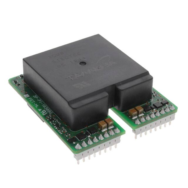
Gate Driver 2DMB51507CC
■Overview
Gate driver 2DMBxxxxxCC is a dual channel gate driver designed for IGBT and SiC MOSFET.
The high breakdown voltage and low parasitic capacitance make it suitable for gate drives
such as SiC MOSFET and IGBT.
■Features
・Ideal for drive of IGBT and SiC MOSFET
・Gate voltage : +15V/-15V
・ALL-IN-ONE (Built-in isolated DC / DC converter and gate drive circuit)
・Low parasitic capacitance (about 12pF) ; highly resistant to common-mode noise.
・Fast response : about 100nsec(typ)
・The gate drive circuit used a isolator.
・Input-to-Output dielectric withstand voltage : AC5000V
・Output CH1-to-Ouput CH2 dielectric withstand voltage : AC4000V
・Input-to-Output insulation distance : 14mm (clearance・creepage)
・Output CH1-to-Output CH2 insulation distance : 7mm (clearance), 12mm(creepage)
・DC/DC converter input voltage :13~28V
・Signal input voltage : 3.3V,5V
・Overload protection (DC/DC converter)
・Overheat protection (DC/DC converter)
・Half bridge mode (Gate drive circuit)
・Desaturation protection (Gate drive circuit)
・Soft turn-off function (Gate drive circuit)
・Fault signal output function (Gate drive circuit)
・Miller clamp function (Gate drive circuit)
・Under-voltage lockout(UVLO) (Gate drive circuit)
・Safety satndards : UL508 (certification pending)
■Application
Industrial inverter, power conditioner, etc …
■Ciruit Image
2DMBxxxxxCC
15V
24V
3.3V
5V
1 VIN+
2 VIN3
4
5
6
VCC
DTC1
DTC2
ALM1
7 ALM2
8 MODE
9 RTC
10 INA
11 INB
12 GND
1 / 13
DST2
VO1+
VGH2
VGL2
STO2
MCL2
E/S2
24
27
28
29
30
31
26
VO2- 25
DST1
VO1+
VGH1
VGL1
STO1
MCL1
E/S1
VO1-
20
17
16
15
14
13
18
19
TAMURA CORPORATION
TMRDM0027EN
Rev.0.04 Dec, 2019
�2DMB51507CC Datasheet
CONFIDENTIAL
■Internal Block Diagram
VIN+
VIN-
VCC
VO2+
DST2
VGH2
VGL2
STO2
MCL2
E/S2
VO2-
DESAT detection
INB
Isolator
LOGIC
ALM2
Soft-turn off
1k
Miller Clamp
LOGIC
RTC
Timer
DC/DC converter
Gate Drive Ch2
VO1+
COM1
VIN+
DTC1
VO1-
VIN-
DTC2
Overheat
protection
Overload
protection
Direct
/
Halfbridge
MOD
VO2+
COM2
VO2-
Gate Drive Ch1
1k
VO1+
DST1
VGH1
VGL1
STO1
MCL1
E/S1
VO1-
DESAT detection
INA
Isolator
LOGIC
ALM1
Soft-turn off
Miller Clamp
1k
GND
■Pin Connection
Input
Output
Pin No.
Name
Pin No.
Name
CH
1
VIN+
Common
2
VIN-
Common
Power supply for DC/DC converter(+)
13
MCL1
1
Miller clamp pin
Power supply for DC/DC converter(-)
14
STO1
1
Soft turn off pin
3
VCC
4
DTC1
-
Power supply for drive circuit
15
VGL1
1
Gate OFF side pin
1
Dead time adjustment
16
VGH1
1
Gate ON side pin
5
6
DTC2
2
Dead time adjustment
17
VO1+
1
DC/DC converter output pin
ALM1
1
Alarm signal output
18
E/S1
1
7
Emitter・source connection pin
ALM2
2
Alarm signal output
19
VO1-
1
DC/DC converter output pin
8
MOD
-
Mode select
20
DST1
1
Desaturation protection pin
9
RTC
-
Recovery time of protection circuit control
21
NONE
-
None
10
INA
1
Control input A
22
NONE
-
None
11
INB
2
Control input B
23
NONE
-
None
12
GND
-
Ground for drive circuit
24
DST2
2
Desaturation protection pin
25
VO2-
2
DC/DC converter output pin
26
E/S2
2
Emitter・source connection pin
27
VO1+
2
DC/DC converter output pin
28
VGH2
2
Gate ON side pin
29
VGL2
2
Gate OFF side pin
30
STO2
2
Soft turn off pin
31
MCL2
2
Miller clamp pin
2 / 13
Function
TAMURA CORPORATION
Function
TMRDM0027EN
Rev.0.04 Dec, 2019
�2DMB51507CC Datasheet
CONFIDENTIAL
■I/O Condition Table
No.
Status
1
VO1+,VO2+
UVLO
Input
Output(CH1)
VO+ DST1 DST2 MOD INA
Output(CH2)
INB ALM1 VGH1 VGL1 STO1 MLC1 ALM2 VGH2 VGL2 STO2 MLC2
UVLO
X
X
X
X
X
L
○
X
L
L
X
L
X
X
X
X
X
Hi-Z Hi-Z
○
X
L
L
X
H
X
X
X
X
X
Hi-Z
H
○
L
X
L
L
X
Hi-Z Hi-Z
L
L
L
X
X
X
X
X
5
○
L
X
L
H
X
Hi-Z
X
X
X
X
X
6
○
L
L
H
X
L
Hi-Z Hi-Z
L
L
L
Hi-Z Hi-Z
L
L
L
○
L
L
H
L
H
Hi-Z Hi-Z
L
L
L
Hi-Z
2
3
4
7
8
Normal
operation
Normal
operation
(HBM)
Hi-Z Hi-Z Hi-Z Hi-Z
H
Hi-Z Hi-Z Hi-Z
L
Hi-Z Hi-Z Hi-Z Hi-Z
H
L
L
Hi-Z Hi-Z Hi-Z
Hi-Z Hi-Z Hi-Z
○
L
L
H
H
H
Hi-Z
H
L
L
9
○
L
Hi-Z
L
X
L
Hi-Z
X
X
X
X
L
Hi-Z Hi-Z
L
L
10 Desaturation
11 protection1
○
L
Hi-Z
L
X
H
Hi-Z
X
X
X
X
L
Hi-Z Hi-Z
L
L
○
L
Hi-Z
H
L
H
Hi-Z Hi-Z
L
L
L
L
Hi-Z Hi-Z
L
L
12
○
L
Hi-Z
H
H
H
Hi-Z
L
Hi-Z Hi-Z
L
L
13
○
Hi-Z
L
L
L
X
L
Hi-Z Hi-Z
L
L
Hi-Z
X
X
X
X
14 Desaturation
15 protection2
○
Hi-Z
L
L
H
X
L
Hi-Z Hi-Z
L
L
Hi-Z
X
X
X
X
○
Hi-Z
L
H
L
H
L
Hi-Z Hi-Z
L
L
Hi-Z
H
16
○
Hi-Z
L
H
H
H
L
Hi-Z Hi-Z
L
L
Hi-Z Hi-Z
H
Hi-Z Hi-Z Hi-Z Hi-Z Hi-Z
L
Hi-Z Hi-Z Hi-Z
L
Hi-Z Hi-Z Hi-Z
L
L
L
○ : VO UVLO > UVLO, X : Don't care
3 / 13
TAMURA CORPORATION
TMRDM0027EN
Rev.0.04 Dec, 2019
�2DMB51507CC Datasheet
CONFIDENTIAL
■Absolute Maximum Ratings
Item
Symbol
Min
VIN
VCC,VSG
VSG
Input voltage for DC/DC converter
Input-side signal voltage
Max
Unit
Conditions・Note
-0.3
28
Vdc
-0.3
5.5
V
VCC, RTC, MOD, INA, INB
-0.3
28
V
ALM1, ALM2
ALM1, ALM2
Between VIN+ to VIN-
ISG
-
5
mA
DESAT pin input voltage
VDESAT
-0.3
VGH+0.3
V
Miller clamp pin input voltage
VCLAMP VGL-0.3 VGH+0.3
V
Maximum gate current
IGPEAK
-
43
A
Guaranteed by design
DC/DC converter output power
POUT
-
3.3
W
Per output circuit
Switching frequency
FSW
-
150
kHz
Operating temperature range
TOP
-40
85
℃
Operating humidity
RHOP
20
95
%RH
Storage temperature range
TSTG
-40
90
℃
Storage humidity
RHSTG
5
95
%RH
Input-side signal maximum current
See the derating curve
No condensation
No condensation
■Recommended Operating Conditons
Item
Symbol
Min
Max
Unit
VIN
13.5
26.4
Vdc
VCC,VSG
3
5.5
Vdc
N
-
2
-
Logic high level input voltage
VSGH
VCC x0.7
-
V
MOD, INA, INB
Logic low level input voltage
VSGL
-
VCC x0.3
V
MOD, INA, INB
ISG
5
-
mA
MOD, INA, INB VSG=5V
150 kHz)
QMAX
-
210
nC
IGAVE= 110mA Reference value
30 kHz)
QMAX
-
5000
nC
IGAVE= 110mA Reference value
QG
-
8000
nC
tINMSK
80
-
ns
Input voltage range for DC/DC converter
Input-side signal voltage range
Driver circuit number
Source current of control signal
Maximum gete drive capability
(
Maximum gete drive capability
(
Maximum gete charge amount
Minimum input pulse width
Conditions・Note
■Derating Curve
Reduce the output power according to the following derating table.
8000
7000
6000
Qg[nC]
5000
4000
3000
Ta:-40~+85℃ / VIN = 13.5~18V
Ta:-40~+75℃ / VIN = 18~26.4V
2000
1000
Ta:-40~+60℃ / VIN = 13.5~26.4V
0
0
50
100
150
Frequency[kHz]
4 / 13
TAMURA CORPORATION
TMRDM0027EN
Rev.0.04 Dec, 2019
�2DMB51507CC Datasheet
CONFIDENTIAL
■Electrical Specification (Vin=24V, Vcc=5V.Ta=25℃, Unless otherwise specified)
DC/DC converter block
Symbol
Min
Typ
Max
Unit
Start-up voltage
Item
VSTART
-
-
13
V
Conditions・Note
Max input current
IINMAX
-
0.45
-
A
Fsw=30kHz /Ta:60℃
Standby power
PSTBY
-
1.4
-
W
No load
Symbol
Min
Typ
Max
Unit
Logic high level input voltage
VSGH
VCC x0.7
-
-
V
MOD, INA, INB
Logic low level input voltage
VSGL
-
-
VCC x0.3
V
INA, INB
Logic pull-down resistance
RSGD
-
1000
-
Ω
INA, INB
Gate drive block
Item
Conditions・Note
Logic
Output
Gate ON side pin voltage
VGH
14
15
16
V
No load
Gate OFF side pin voltage
VGL
-16
-15
-14
V
No load
Miller clamp voltage
VCLAMP
-
1.2
-
V
ICLAMP=500mA, Guaranteed by design
Miller clamp ON threshold voltage
VCLPON
-
VGL+2
-
V
tPON
-
100
-
ns
ns
Delay time
Turn ON time
tPOFF
-
100
-
Dead time
tDEAD
-
4.1
-
us
Common-mode transient immunity
CMTI
-
-
70
kV/us
Symbol
Min
Typ
Max
Unit
Turn OFF time
Half bridge mode
■Protection
DC/DC converter block
Item
Conditions・Note
Overload protection
-
8.8
-
-
W
Auto recovery
Overheat protection
-
120
-
150
℃
Auto recovery,CASE temperature
Symbol
Min
Typ
Max
Unit
VUVLOGHH
13.2
13.5
13.8
V
Gate ON side UVLO OFF voltage VUVLOGHL
12.2
12.5
12.8
V
uA
Gate drive block
Item
Gate ON side UVLO ON voltage
Conditions・Note
IDESAT
200
240
280
VSD
6.0
6.35
7.0
V
DESAT detection filter time
tDSTFIL
-
300
-
ns
Guaranteed by design
DESAT detection time
tDSTOUT
-
350
-
ns
Guaranteed by design
Alarm signal output L voltage
VALML
-
-
0.5
V
IALM=5mA
tALM
-
550
-
ns
tRESTART
-
110
-
ms
tSTO
-
4
-
us
DESAT charge current
DESAT detection voltage
Alarm signal output time
Restart time
Soft turn off duration
5 / 13
TAMURA CORPORATION
TMRDM0027EN
Rev.0.04 Dec, 2019
�2DMB51507CC Datasheet
CONFIDENTIAL
■Insulation
Item
Specification
Conditions・Note
Between Input-Output
Dielectric withstand voltage
AC5000V
1min, Cutoff 2mA
Insulation resistance
100MΩ or more
DC500V
Minimum clearance distances
14mm
Minimum creepage distances
14mm
Partial discharge extinction volt.
1768Vpeak or more
According to EN50178/IEC 60270
Dielectric withstand voltage
AC4000V
1min, Cutoff 2mA
Insulation resistance
100MΩ or more
DC500V
Minimum clearance distances
7mm
Minimum creepage distances
12mm
Partial discharge extinction volt.
1700Vpeak or more
Between CH1-CH2
6 / 13
TAMURA CORPORATION
According to EN50178/IEC 60270
TMRDM0027EN
Rev.0.04 Dec, 2019
�2DMB51507CC Datasheet
CONFIDENTIAL
■Pin Function
・Vin(+), Vin(-) (Power supply pin for DC/DC converter)
・VCC(Power supply pin for drive curcuit)
・GND(Ground pin for drive curcuit)
・MOD, INA, INB(Mode switching pin, Control input pin) (*Note1)
The INA, INB and MOD pin is a pin used to determine output logic.
Direct mode / Half bridge mode can be switched by MOD pin.
In Half bridge mode, it functions as INA: gate signal, INB: enable signal.
MOD
INA
INB
Gate G1
Gate G2
L
L
X
L
X
L
H
X
H
X
L
X
L
X
L
L
X
H
X
H
H
X
L
L
L
H
L
H
L
H
H
H
H
H
L
Mode
Direct mode
Half bridge mode
MOD
H
L
INA
H
L
INB
H
L
Gate G1
H
L
Gate G2
H
L
Timing chart of Direct mode
MOD
H
L
INA
H
L
INB( Ena ble)
H
L
Gate G1
H
L
Gate G2
H
L
t DEAD
Output enable
Timing chart of Half bridge mode
・DTC1,2(Dead time adjustment pin)
When half-bridge mode, this pin is adjust the dead time of gate output G1,G2
・RTC(Recovery time of protection circuit control pin)
When abnormality occurs (UVLO, short circuit detected),this pin is used to adjust the recovery time.
7 / 13
TAMURA CORPORATION
TMRDM0027EN
Rev.0.04 Dec, 2019
�2DMB51507CC Datasheet
CONFIDENTIAL
・ALM1,2(Alarm signal output pin)
When abnormality occurs (UVLO, short circuit detected),This pin outputs an alarm signal. (Open-Drain)
Status
ALM1,2
While in normal operation
Hi-Z
UVLO, When detecting short circuit
L
・MCL1,2(Miller clamp pin)
The MCL pin is a pin for preventing inrease in gate voltage due to the miller current of the power device connected to Gate pin.
・VGL1,2(Gatte OFF side pin)
The VGL pin is a pin for gate drive of low signal. VGL pin connect to the gate pin through gate resistor of OFF side.
・DST1,2(Desaturaion protection pin)
The DESAT pin is a pin used to detect desaturation. When the DESAT pin voltage exceeds VDESAT, the DESAT function will be
activated. This may cause the IC to malfunction in an open state. To avoid such trouble, short-circuit the DESAT pin to the E/S
pin if the desaturation protection is not used. In order to prevent the wrong detection due to noise, the noise mask time tDESATFIL
is set.
・E/S1,2(Emitter/source pin)
E/S pin connect to the emitter / source of the power device.
・VGH1,2(Gate ON side pin)
The VGH pin is a pin for gate drive of high signal. VGH pin connect to the gate pin through gate resistor of ON side.
・STO1,2(Soft turn off pin)
The STO pin is a pin for gradually decrease gate voltage in operating desaturation protection.
STO pin connect to the gate pin though a resistance value higher than the resistance value connected to VGL 1 and 2.
・VO1+,VO2+,VO1-,VO2-(DC/DC converter output pin)
The VO+,VO2+,VO1-,VO2- pin is a output pin of built-in DC/DC converter. If necessary, connect a capacitor.
■Description
1. Gate voltage rise prevention function (Miller clamp function)
If gate output Gx=L and the Miller clamp pin voltage < V CLPON, the internal MOSFET of the miller clamp pin turns on.
Gate Gx
MCL
Internal MOSFET of the MCL pin
L
Less than VCLPON
ON
L
Not less than VCLPON
OFF
H
X
OFF
2. Undervoltage Lockout (UVLO) function
The control circuit incorporates the undervoltage lockout (UVLO) function both on the output voltage + sides.
When the output voltage+ drops to the UVLO ON voltage, the gate ON/OFF side pin and the ALM pin both will output the “L”signal.
When the output voltage+ rises to the UVLO OFF voltage, these pins will be reset.
8 / 13
TAMURA CORPORATION
TMRDM0027EN
Rev.0.04 Dec, 2019
�CONFIDENTIAL
2DMB51507CC Datasheet
3. Short circuit protection function, Soft turn-off function
When the collector/drain pin voltage exceeds VSD, the short circuit protection function will be activated.
When the short circuit protection function is activated, the gate ON/OFF side pin will be set to the “Hi-Z” level,
and then the ALM pin voltage to the “L” level.
Also, soft turn-off function works to reduce collector/drain voltage surge due to short circuit current.
Short circuit protection is automatically canceled after the abnormal state recovery time.
INA or INB
H
L
Gate G1 or G2
H
L
VSD
DST1 or DST2
0
H
L
ALM1 or 2
t DSTFIL
t DSTOUT
t ALM
t RESTART
Timing chart of short circuit protection function
*Note1:After input to voltage in Vcc, it input High signal→Low signal in INx then it activate.
Vcc
VCC
9 / 13
0
INA or INB
H
L
Gate G1 or G2
H
L
ALM1 or 2
H
L
TAMURA CORPORATION
TMRDM0027EN
Rev.0.04 Dec, 2019
�2DMB51507CC Datasheet
CONFIDENTIAL
■Reliability
Item
Test condition and acceptance criterion
Exposure in high temperature
90℃, 240H, ※
Exposure in low temperature
-40℃, 240H, ※
Exposure in high temperature and high humidity
60℃, 90~95%RH, 240H, ※
Thermal shock
-40℃/30min to 100℃/30min, 500cycles, ※
Low temperature operation
Input voltage:DC24V, Output current:Rated Load
-40℃, 240H, ※
High temperature operation
Input voltage:DC24V, Output current:Rated Load
85℃, 240H, ※
high temperature
Input voltage:DC24V, Output current:Rated Load
and high humidity operation
85℃, 85%RH, 240H, ※
Vibration
Vibration amplitude:1.5mm(peak to peak), Vibration Frequency:10 to 55Hz, Sweeping:1min.
In each X,Y and Z direction:once, 120min. ※
Impact
Acceleration:490m/s2 (50G), Operating time:11ms
In each ±X,Y and Z direction:3 times, ※
Drop test for packaged freights
Dorp to concrete.
Height:40cm
Dorp surface:1 corner, 3 spines, 6 surfaces, 1 time each.
Solderblity
Sample shall be dipped into the solution of Methanol and Rosin
(having 75% Methanol and having 25% Rosin by weight measuring)
and shall be dippend into the solder bath having the solder Sn-3Ag-0.5Cu
of 250±5℃ to the position to 3mm from the end of terminal for 3.0±0.5 seconds,
and pulled up. After above treatment, the sample shall be coveredby solder uniformly
at more than 75% of circumference and shall not show any unusual appearance.
Resistance to soldering heat
Sample shall be dipped into the solution of Methanol and Rosin
(having 75% Methanol and having 25% Rosin by weight measuring)
and shall be dippend into the solder bath having the solder Sn-3Ag-0.5Cu
of 260±5℃ to the position to 3mm from the end of terminal for 10.0±0.5
seconds, and pulled up. After that sample shall be replace in normal ambient
for 1~2 hours and shall not show any unusual appearance.
※After each test, exposure at room temperature and humidity condition for 24 hours.
There shall be no abnormality on the electrical specification and appearance.
10 / 13
TAMURA CORPORATION
TMRDM0027EN
Rev.0.04 Dec, 2019
�2DMB51507CC Datasheet
CONFIDENTIAL
■Outline Dimensional Drawing
Unit:mm
Note :1.The dimensional tolerance without directions is ± 0.5mm.
■Product Weight
45g(TYP)
11 / 13
TAMURA CORPORATION
TMRDM0027EN
Rev.0.04 Dec, 2019
�2DMB51507CC Datasheet
CONFIDENTIAL
■Recommended Soldering Condition
・Flow soldering condition
: 255±3℃ Less than 3sec
Temperature of preheating 110℃~130℃
End temperature of preheating 110℃±10℃
・Soldering condition of hand work
: 360℃(MAX) Less than 3sec
■Storage Conditions
Item
Storage temperature
Min
Max
Unit
-25
60
℃
Conditions・Note
A packing state
※If you want to use past the long period there is a concern that the solder non-wetting by terminal oxidation to occur.
Therefore, please use from taking enough tests.
■Usage Cautions
● Always mount fuse on the plus side of input for ensuring safety because the fuse is not built-in the product.
Please select the fuse considering conditions such as steady current, inrush current, and ambient temperature.
When using a fuse having large rated current or high capacity input electrolytic condenser, by combining
another converter and input line and input electrolytic condenser, fuse may not blow off in the case of abnormality.
Do not combine high voltage line and fuse.
● Make sure the rise/fall time of the input signal is 500ns or less.
● Please do not apply excessive stress to this product when attaching to power module.
12 / 13
TAMURA CORPORATION
TMRDM0027EN
Rev.0.04 Dec, 2019
�CONFIDENTIAL
2DMB51507CC Datasheet
■Important Notice
● The content of this information is subject to change without prior notice for the purpose of improvements, etc.
Ensure that you are in possession of the most up-to-date information when using this product.
● The operation examples and circuit examples shown in this document are for reference purposes only, and TAMURA Corporation disclaims
all responsibility for any violations of industrial property rights, intellectual property rights and any other rights owned by TAMURA Corporation
or third parties that these may entail.
● The circuit examples and part constants listed in this document are provided as reference for the verification of
characteristics. You are to perform design, verification, and judgment at your own responsibility, taking into account the various conditions.
● TAMURA has evaluated the efficiency and performance of this product in a usage environment determined by us.
Depending on your usage environment or usage method, there is the possibility that this product will not perform sufficiently as shown in
the specifications, or may malfunction.
When applying this product to your devices or systems, please ensure that you conduct evaluations of their state when integrated with
this product. You are responsible for judging its applicability.
TAMURA bears no responsibility whatsoever for any problems with your devices,
systems or this product which are caused by your usage environment or usage method.
● TAMURA Corporation constantly strives to improve quality and reliability, but malfunction or failures are bound to occur with some
probability in power products. To ensure that failures do not cause accidents resulting in injury or death, fire accidents, social damage,
and so on, you are to thoroughly verify the safety of their designs in devices and/or systems, at your own responsibility.
● This product is intended for use in consumer electronics (electric home appliances, business equipment, Information equipment, communication
terminal equipment, measuring devices, and so on.) If considering use of this product in equipment or devices that require high reliability
(medical devices, transportation equipment, traffic signal control equipment, fire and crime prevention equipment, aeronautics and space
devices, nuclear power control, fuel control, in-vehicle equipment, safety devices, and so on), please consult a TAMURA sales representative
in advance. Do not use this product for such applications without written permission from TAMURA Corporation.
● This product is intended for use in environments where consumer electronics are commonly used.
It is not designed for use in special environments such as listed below, and if such use is considered,
you are to perform thorough safety and reliability checks at your own responsibility.
・ Use in liquids such as water, oil, chemical solutions, or organic solvents, and use in locations
where the product will be exposed to such liquids.
・ Use that involves exposure to direct sunlight, outdoor exposure, or dusty conditions.
・ Use in locations where corrosive gases such as salt air, C12, H2S, NH3, SO2, or NO2, are present.
・ Use in environments with strong static electricity or electromagnetic radiation.
・ Use that involves placing inflammable material next to the product.
・ Use of this product either sealed with a resin filling or coated with resin.
・ Use of water or a water soluble detergent for flux cleaning.
・ Use in locations where condensation is liable to occur.
● This product is not designed to resist radiation.
● This product is not designed to be connected in series or parallel.
Do not operate this product in a series, parallel, or N+1 redundant configuration.
● Do not use or otherwise make available the TAMURA products or the technology described in this document for any military purposes,
including without limitation, for the design, development, use, stockpiling or manufacturing of mass destruction weapons
(e.g. nuclear, chemical, or biological weapons or missile technology products).
When exporting and re-exporting the products or technology described in this document, you should comply with the applicable export
control laws and regulations and follow the procedures required by such laws and regulations including, without limitation,
Japan -Foreign Exchange and Foreign Trade Control Law and U.S.- Export Administration Regulations.
The TAMURA products and related technology should not be used for or incorporated into any products or systems whose manufacture,
use, or sale is prohibited under any applicable domestic or foreign laws or regulations.
● Please contact your TAMURA sales office for details as to environmental matters such as the RoHS compatibility of product.
Please use TAMURA products in compliance with all applicable laws and regulations that regulate the inclusion or use of controlled substances,
including without limitation, the EU RoHS Directive.
TAMURA assumes no liability for damages or losses occurring as a result of your noncompliance with applicable laws and regulations.
● TAMURA assumes no liability for damages or losses incurred by you or third parties as a result of unauthorized use of TAMURA products.
● This document and any information herein may not be reproduced in whole or in part without prior written permission from TAMURA.
13 / 13
TAMURA CORPORATION
TMRDM0027EN
Rev.0.04 Dec, 2019
�