SLG59M1730C
An Ultra-small 33 mΩ, 1.0 A pFET Load Switch
with Controlled Inrush Current Profile
����
General Description
Pin Configuration
Pin A1 Index Mark
1
Using a proprietary MOSFET design, the SLG59M1730C
achieves a low RDSON across the entire input voltage range.
Through the application of Renesas’s proprietary CuFET
technology, the SLG59M1730C’s can be used in applications
up to 1 A with a very-small 0.64 mm2 WLCSP form factor.
ON
A
VIN
B
SLG59M1730C
Operating from a 2.5 V to 5.5 V power supply, the
SLG59M1730C is a self-powered, high-performance 33 mΩ,
1.0 A single-channel pFET load switch with a controlled VIN
inrush current profile. The SLG59M1730C’s low supply current
and controlled VIN inrush current profile makes it an ideal
pFET integrated load switch in small form-factor personal
health monitor and watch applications.
2
GND
VOUT
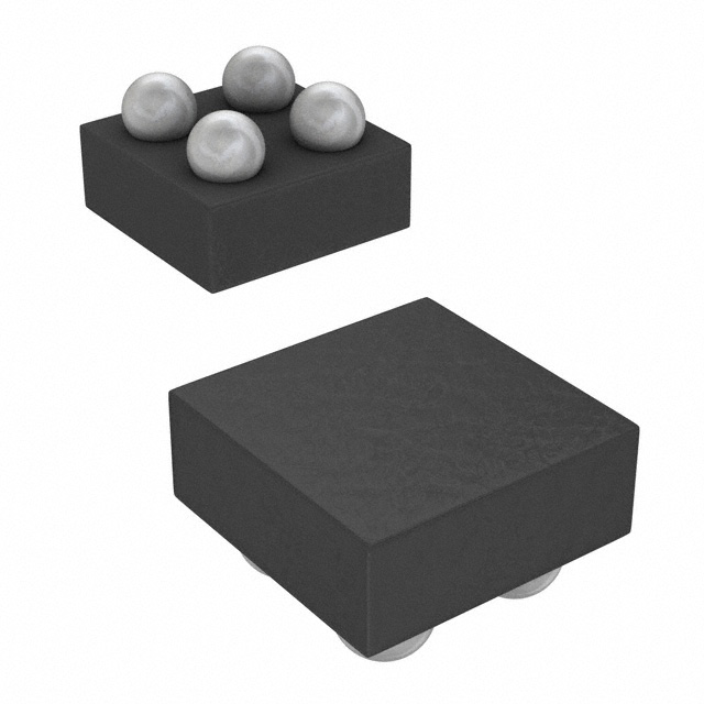
4L WLCSP
(Laser Marking View)
Features
• Integrated 1 A Continuous IDS pFET Load Switch
• Low Typical RDSON:
• 33 mΩ at VIN = 5.5 V
• 45.1 mΩ at VIN = 3.3 V
• 56.1 mΩ at VIN = 2.5 V
• Input Voltage: 2.5 V to 5.5 V
• Low Typical No-load Supply Current: 0.004 µA
• Integrated VOUT Discharge Resistor
• Operating Temperature: -40 °C to 85 °C
• Low θJA, 4-pin 0.8 mm x 0.8 mm, 0.4 mm pitch 4L WLCSP
Packaging
• Pb-Free / Halogen-Free / RoHS compliant
Block Diagram
1.0 A
VIN
VOUT
CIN
30 µF
CLOAD
30 µF
In-rush
Current
Limiting
ON
ON
OFF
©2022 Renesas Electronics Corporation
000-0059M1730-105
Rev 1.05
Revised February 14, 2022
�SLG59M1730C
����
Pin Description
Pin #
Pin Name
Type
Pin Description
Input
A low-to-high transition on this pin initiates the operation of the SLG59M1730C. ON is
an asserted HIGH, level-sensitive CMOS input with VIL < 0.3 V and VIH > 0.85 V. As
the ON pin input circuit does not have an internal pull-down resistor, connect this pin
to a general-purpose output (GPO) of a microcontroller, an application processor, or a
system controller – do not allow this pin to be open-circuited. In order to activate the
SLG59M1730C’s controlled inrush current control circuitry, ON shall be toggled HIGH
only after VIN is higher than the SLG59M1730C’s VSUCC(TH) specification.
A1
ON
B1
VIN
Input terminal connection of the p-channel MOSFET. Connect a 10 µF (or larger)
MOSFET low-ESR capacitor from this pin to ground. Capacitors used at VIN should be rated at
10 V or higher.
B2
VOUT
Output terminal connection of the p-channel MOSFET. For optimal operation of the
MOSFET SLG59M1730C controlled inrush current profile, connect a 30 µF (or smaller) capacitor
from this pin to ground. Capacitors used at VOUT should be rated at 10 V or higher.
A2
GND
GND
Ground connection. Connect this pin to system analog or power ground plane.
Ordering Information
Part Number
Type
Production Flow
SLG59M1730C
WLCSP 4L
Industrial, -40 °C to 85 °C
SLG59M1730CTR
WLCSP 4L (Tape and Reel)
Industrial, -40 °C to 85 °C
000-0059M1730-105
Page 2 of 18
�SLG59M1730C
����
Absolute Maximum Ratings
Parameter
VIN
VOUT to GND
ON to GND
TS
Description
Conditions
Min.
Typ.
Max.
Unit
--
--
6
V
Load Switch Output Voltage to
GND
-0.3
--
VIN
V
ON Pin Voltage to GND
-0.3
--
VIN
V
Load Switch Input Voltage
-65
--
140
°C
ESDHBM
ESD Protection
Human Body Model
2000
--
--
V
ESDCDM
ESD Protection
Charged Device Model
1000
--
--
V
MSL
θJA
WDIS
Storage Temperature
Moisture Sensitivity Level
Package Thermal Resistance,
Junction-to-Ambient
1
0.8 x 0.8 mm 4L WLCSP; Determined
using a 1 in2, 2 oz .copper pad under each
VIN and VOUT terminal and FR4 pcb
material.
Package Power Dissipation
MOSFET IDSPK Peak Current from VIN to VOUT
Maximum pulsed switch current, pulse
width < 1 ms, 1% duty cycle
--
110
--
°C/W
--
--
0.5
W
--
--
1.5
A
Note: Stresses greater than those listed under “Absolute Maximum Ratings” may cause permanent damage to the device. This is a stress rating
only and functional operation of the device at these or any other conditions above those indicated in the operational sections of this
specification is not implied. Exposure to absolute maximum rating conditions for extended periods may affect reliability.
Electrical Characteristics
TA = -40 °C to 85 °C (unless otherwise stated)
Parameter
VIN
IIN
ION_LKG
Description
Conditions
Load Switch Input Voltage
-40 °C to 85 °C
Load Switch Current (Pin B1)
See Note 1
ON Pin Input Leakage
000-0059M1730-105
Min.
Typ.
Max.
Unit
2.5
--
5.5
V
When OFF, VIN = 5.5 V, No load
--
0.110
1.270
µA
When OFF, VIN = 5.0 V, No load
--
0.031
0.880
µA
When OFF, VIN = 3.8 V, No load
--
0.006
0.440
µA
When OFF, VIN = 3.3 V, No load
--
0.004
0.420
µA
When OFF, VIN = 2.5 V, No load
--
0.003
0.390
µA
When ON, ON = VIN = 5.5 V, No load
--
0.006
0.220
µA
When ON, ON = VIN =5.0 V, No load
--
0.004
0.190
µA
When ON, ON = VIN = 3.8V, No load
--
0.003
0.110
µA
When ON, ON = VIN = 3.3 V, No load
--
0.003
0.100
µA
When ON, ON = VIN = 2.5 V, No load
--
0.002
0.070
µA
When ON, ON = 1.8 V, VIN = 5.5 V,
No load
--
0.900
1.100
µA
When ON, ON = 1.8 V, VIN = 5.0 V,
No load
--
0.660
0.830
µA
When ON, ON = 1.8 V, VIN = 3.8 V,
No load
--
0.210
0.330
µA
When ON, ON = 1.8 V, VIN = 3.3 V,
No load
--
0.100
0.220
µA
When ON, ON = 1.8 V, VIN = 2.5 V,
No load
--
0.005
0.110
µA
--
--
0.1
µA
Page 3 of 18
�SLG59M1730C
����
Electrical Characteristics (continued)
TA = -40 °C to 85 °C (unless otherwise stated)
Parameter
RDSON
RDSON
Description
ON Resistance @ TA 25°C
ON Resistance @ TA 85°C
MOSFET IDS Current from VIN to VOUT
VSUCC(TH)
Conditions
Min.
Typ.
Max.
@ 5.5 V, IDS = 100 mA
--
33
41
mΩ
@ 3.3 V, IDS = 100 mA
--
45.1
55
mΩ
@ 2.5 V, IDS = 100 mA
--
56.1
69
mΩ
@ 5.5 V, IDS = 100 mA
--
40.2
49
mΩ
@ 3.3 V, IDS = 100 mA
--
54.5
66
mΩ
@ 2.5 V, IDS = 100 mA
--
68.2
82
mΩ
Continuous
--
--
1.0
A
--
0.9 x VIN
--
V
ON ≥ VON_VIH;
VIN Inrush Current Start-up Control
See Timing Diagram on Page 5 and
Threshold Voltage
Note 1
Unit
Rise Time Charging Current
10% VOUT to 90% VOUT ↑;
VIN = 5.0 V, CLOAD = 30 µF,
See Note 1
11
16.5
25
mA
Slew Rate
10% VOUT to 90% VOUT ↑;
VIN = 5.0 V, CLOAD = 30 µF
0.36
0.54
0.8
V/ms
10% VOUT to 90% VOUT ↑
VIN = 5.0 V, CLOAD = 30 µF,
no RLOAD
5
7.6
11
ms
10% VOUT to 90% VOUT ↑
VIN = 2.5 V, CLOAD = 30 µF,
no RLOAD
2.5
3.8
5.5
ms
VON_VIH to 90% VOUT ↑
VIN = 5 V, CLOAD = 30 µF,
No RLOAD
6
8.6
12
ms
VON_VIH to 90% VOUT ↑
VIN = 2.5 V, CLOAD = 30 µF,
No RLOAD
3
4.3
6
ms
OFF Delay Time
VON_VIL to VOUT Fall, VIN = 5 V,
RLOAD=10 Ω, no CLOAD
--
4.5
--
µs
Output Load Capacitance
CLOAD connected from VOUT to
GND
--
--
30
µF
RDIS
Discharge Resistance
VIN = 2.5 V to 5.5 V, VOUT = 0.4 V
Input Bias
53
90
150
Ω
ON_VIH
Initial Turn On Voltage
0.85
--
VIN
V
ON_VIL
Low Input Voltage on ON pin
-0.3
0
0.3
V
IRISE
VOUT(SR)
TRISE
TTotal_ON
TOFF_Delay
CLOAD
Rise Time
Total Turn On Time
Notes:
1. Rise of ON pin must only occur after VIN reaches VSUCC(TH) in order to have proper in-rush current limiting and start-up.
000-0059M1730-105
Page 4 of 18
�SLG59M1730C
����
TTotal_ON, TON_Delay and Slew Rate Measurement
VSUCC(TH)
VIN
ON*
VON_VIH
VON_VIL
TOFF_Delay
TTotal_ON
90% VOUT
90% VOUT
VOUT
10% VOUT
10% VOUT
TRISE
TFALL
* VIN ≥ 90% Nominal Voltage before Asserting ON Signal
RDSON vs. Temperature and VIN
000-0059M1730-105
Page 5 of 18
�SLG59M1730C
����
IIN when ON vs. VIN and Temperature
IIN when ON = 1.8 V vs. VIN and Temperature
000-0059M1730-105
Page 6 of 18
�SLG59M1730C
����
IIN when OFF vs. VIN and Temperature
TRISE vs. CLOAD, Temperature, and VIN
000-0059M1730-105
Page 7 of 18
�SLG59M1730C
����
TTotal_ON vs. CLOAD, Temperature, and VIN
VIN vs. Max IDS, Safe Operation Area
8
7
6
5
VIN (V)
4
SOA
Boundary
3
2
1
0
0
0.5
1
1.5
2
Max IDS (A)
000-0059M1730-105
Page 8 of 18
�SLG59M1730C
����
Typical Turn-on Waveforms
Figure 1. Typical Turn ON operation waveform for VIN = 2.5 V, CLOAD = 30 μF
Figure 2. Typical Turn ON operation waveform for VIN = 5 V, CLOAD = 30 μF
000-0059M1730-105
Page 9 of 18
�SLG59M1730C
����
Typical Turn-off Waveforms
Figure 3. Typical Turn OFF operation waveform for VIN = 2.5 V, no CLOAD , RLOAD = 10 Ω
Figure 4. Typical Turn OFF operation waveform for VIN = 2.5 V, CLOAD = 30 μF, RLOAD = 10 Ω
000-0059M1730-105
Page 10 of 18
�SLG59M1730C
����
Figure 5. Typical Turn OFF operation waveform for VIN = 5 V, no CLOAD , RLOAD = 10 Ω
Figure 6. Typical Turn OFF operation waveform for VIN = 5 V, CLOAD = 30 μF, RLOAD = 10 Ω
000-0059M1730-105
Page 11 of 18
�SLG59M1730C
����
Applications Information
SLG59M1730C Nominal Operation
During VIN power-up operation, the SLG59M1730C’s internal inrush current Start-up Control circuit is activated once VIN reaches
90% of its nominal voltage (Please see VSUCC(TH) specification). Once VIN has reached this threshold (within the SLG59M1730C’s
nominal input range of 2.5 V to 5.5 V), the ON pin can be toggled LOW-to-HIGH to close the switch. Nominal power-off sequence
is performed in reverse: that is, the ON pin is toggled HIGH-to-LOW to open the switch before VIN is powered down/turned OFF.
SLG59M1730C VIN Inrush Current Limit on Startup
During startup, the current passing through the power FET is internally limited to a maximum specified by IRISE in the EC table.
To prevent incomplete start-up, the SLG59M1730C shall be powered up only with a capacitive load CLOAD attached to the VOUT
pin. After VOUT ramps up to its nominal voltage, a resistive load (RLOAD) can be applied to the integrated load SWITCH.
Slew Rate Calculation
During the rise of VOUT, the SLG59M1730C limits the output current to IRISE. With a capacitor CLOAD attached to VOUT, the
equation below provides the nominal value for the slew rate:
Slew Rate =
IRISE
CLOAD
Power Dissipation Considerations
The junction temperature of the SLG59M1730C depends on factors such as board layout, ambient temperature, external air flow
over the package, load current, and the RDSON-generated voltage drop across each power MOSFET. While the primary
contributor to the increase in the junction temperature of the SLG59M1730C is the power dissipation of its power MOSFETs, its
power dissipation and the junction temperature in nominal operating mode can be calculated using the following equations:
PDTOTAL = RDSON x IDS2
where:
PDTOTAL = Total package power dissipation, in Watts (W)
RDSON= Power MOSFET ON resistance, in Ohms (Ω)
IDS = Output current, in Amps (A)
and
TJ= PDTOTAL x ΘJA + TA
where:
TJ = Die junction temperature, in Celsius degrees (°C)
ΘJA = Package thermal resistance, in Celsius degrees per Watt (°C/W) – highly dependent on pcb layout
TA = Ambient temperature, in Celsius degrees (°C)
In nominal operating mode, the SLG59M1730C’s power dissipation can also be calculated by taking into account the voltage drop
across the switch (VIN - VOUT) and the magnitude of the switch’s output current (IDS):
PDTOTAL = (VIN - VOUT) x IDS or
PDTOTAL = (VIN – (RLOAD x IDS)) x IDS
where:
PDTOTAL = Total package power dissipation, in Watts (W)
VIN = Switch input Voltage, in Volts (V)
RLOAD = Output Load Resistance, in Ohms (Ω)
IDS = Switch output current, in Amps (A)
VOUT = Switch output voltage, or RLOAD x IDS
000-0059M1730-105
Page 12 of 18
�SLG59M1730C
����
Package Top Marking System Definition
Pin 1 Identifier
NN
N
Serial Number Line 1
Serial Number Line 2
NN -Part Serial Number Field Line 1
where each “N” character can be A-Z and 0-9
N - Part Serial Number Field Line 2
where each “N” character can be A-Z and 0-9
000-0059M1730-105
Page 13 of 18
�SLG59M1730C
����
Package Drawing and Dimensions
4 Pin WLCSP Green Package 0.8 x 0.8 mm
000-0059M1730-105
Page 14 of 18
�SLG59M1730C
����
SLG59M1730C 4 Pin WLCSP PCB Landing Pattern
000-0059M1730-105
Page 15 of 18
�SLG59M1730C
����
Recommended Reflow Soldering Profile
For successful reflow of the SLG59M1730C a recommended thermal profile is illustrated below:
Note: This reflow profile is for classification/preconditioning and are not meant to specify board assembly profile. Actual board
assembly profiles should be developed based on specific process needs and board designs and should not exceed parameters
depicted on figure above.
Please see more information on IPC/JEDEC J-STD-020: latest revision for reflow profile based on package volume of 0.352 mm3
(nominal).
000-0059M1730-105
Page 16 of 18
�SLG59M1730C
����
Tape and Reel Specifications
Max Units
Leader (min)
Nominal
Reel &
Package # of
Package Size
Hub Size
Length
Type
Pins
per Reel per Box
Pockets
[mm]
[mm]
[mm]
WLCSP 4L
0.8 x 0.8
mm 0.4P
Green
4
0.8 x 0.8 x 0.44
3000
3000
178/60
100
400
Trailer (min)
Pockets
Length
[mm]
Tape
Width
[mm]
100
400
8
Part
Pitch
[mm]
4
Carrier Tape Drawing and Dimensions
Pocket BTM Pocket BTM Pocket
Package
Length
Width
Depth
Type
WLCSP 4L
0.8 x 0.8 mm
0.4P Green
Index
Hole
Pitch
Pocket Index Hole
Pitch
Diameter
Index Hole Index Hole
to Tape
to Pocket
Edge
Center
Tape
Tape
Width Thickness
A0
B0
K0
P0
P1
D0
E
F
W
T
0.87
0.87
0.56
4
2
1.5
1.75
3.5
8
0.2
Note: 1.Orientation in carrier: Pin1 is at upper left corner (Quadrant 1).
000-0059M1730-105
Refer to EIA-481 specification
Page 17 of 18
�SLG59M1730C
����
Revision History
Date
Version
2/14/2022
1.05
Renesas rebranding
Fixed typos
10/24/2017
1.04
Updated IIN specifications
Updated Charts
7/24/2017
1.03
Updated Tape and Reel Specification
5/5/2 017
1.02
Updated EC Table
3/28/2017
1.01
Fixed typos
Updated PCB Landing Pattern
3/1/2017
1.00
Production Release
000-0059M1730-105
Change
Page 18 of 18
�IMPORTANT NOTICE AND DISCLAIMER
RENESAS ELECTRONICS CORPORATION AND ITS SUBSIDIARIES (“RENESAS”) PROVIDES TECHNICAL
SPECIFICATIONS AND RELIABILITY DATA (INCLUDING DATASHEETS), DESIGN RESOURCES (INCLUDING
REFERENCE DESIGNS), APPLICATION OR OTHER DESIGN ADVICE, WEB TOOLS, SAFETY INFORMATION, AND
OTHER RESOURCES “AS IS” AND WITH ALL FAULTS, AND DISCLAIMS ALL WARRANTIES, EXPRESS OR IMPLIED,
INCLUDING, WITHOUT LIMITATION, ANY IMPLIED WARRANTIES OF MERCHANTABILITY, FITNESS FOR A
PARTICULAR PURPOSE, OR NON-INFRINGEMENT OF THIRD PARTY INTELLECTUAL PROPERTY RIGHTS.
These resources are intended for developers skilled in the art designing with Renesas products. You are solely responsible
for (1) selecting the appropriate products for your application, (2) designing, validating, and testing your application, and (3)
ensuring your application meets applicable standards, and any other safety, security, or other requirements. These
resources are subject to change without notice. Renesas grants you permission to use these resources only for
development of an application that uses Renesas products. Other reproduction or use of these resources is strictly
prohibited. No license is granted to any other Renesas intellectual property or to any third party intellectual property.
Renesas disclaims responsibility for, and you will fully indemnify Renesas and its representatives against, any claims,
damages, costs, losses, or liabilities arising out of your use of these resources. Renesas' products are provided only subject
to Renesas' Terms and Conditions of Sale or other applicable terms agreed to in writing. No use of any Renesas resources
expands or otherwise alters any applicable warranties or warranty disclaimers for these products.
(Rev.1.0 Mar 2020)
Corporate Headquarters
Contact Information
TOYOSU FORESIA, 3-2-24 Toyosu,
Koto-ku, Tokyo 135-0061, Japan
www.renesas.com
For further information on a product, technology, the most
up-to-date version of a document, or your nearest sales
office, please visit:
www.renesas.com/contact/
Trademarks
Renesas and the Renesas logo are trademarks of Renesas
Electronics Corporation. All trademarks and registered
trademarks are the property of their respective owners.
© 2021 Renesas Electronics Corporation. All rights reserved.
�