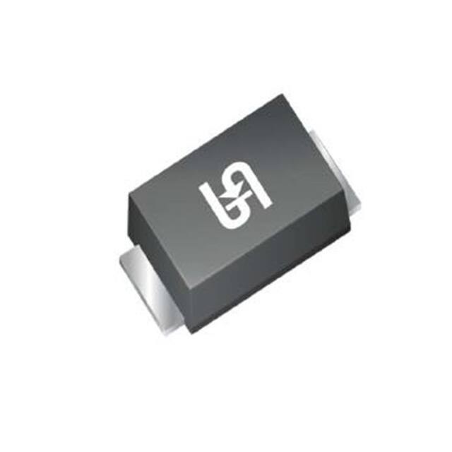
0
登录后你可以
  • 下载海量资料
  • 学习在线课程
  • 观看技术视频
  • 写文章/发帖/加入社区
创作中心
发布
  • 发文章

  • 发资料

  • 发帖

  • 提问

  • 发视频

创作活动
SS115LHMHG

SS115LHMHG

  • 厂商:

    TAIWANSEMICONDUCTOR(台半)

  • 封装:

    Sub-SMA

  • 描述:

    DIODE SCHOTTKY 150V 1A SUB SMA

  • 数据手册
  • 价格&库存
SS115LHMHG 数据手册
SS12L – SS115L Taiwan Semiconductor 1A, 20V - 150V Schottky Barrier Surface Mount Rectifier FEATURES ● ● ● ● ● ● ● KEY PARAMETERS Low power loss, high efficiency Ideal for automated placement Guard ring for overvoltage protection High surge current capability Moisture sensitivity level: level 1, per J-STD-020 RoHS Compliant Halogen-free according to IEC 61249-2-21 PARAMETER VALUE UNIT IF 1 A VRRM 20 - 150 V IFSM 30 A TJ MAX 125, 150 °C APPLICATIONS Package Sub SMA Configuration Single die ● Switching mode power supply (SMPS) ● Adapters ● DC to DC converters MECHANICAL DATA ● ● ● ● ● ● Case: Sub SMA Molding compound meets UL 94V-0 flammability rating Terminal: Matte tin plated leads, solderable per J-STD-002 Meet JESD 201 class 2 whisker test Polarity: Indicated by cathode band Weight: 0.019g (approximately) Sub SMA ABSOLUTE MAXIMUM RATINGS (TA = 25°C unless otherwise noted) PARAMETER SYMBOL Marking code on the device SS 12L SS 13L SS 14L SS 15L SS 16L SS SS SS UNIT 19L 110L 115L 12L 13L 14L 15L 16L 19L 10L A5L Repetitive peak reverse voltage VRRM 20 30 40 50 60 90 100 150 V Reverse voltage, total rms value VR(RMS) 14 21 28 35 42 63 70 105 V Forward current Peak forward surge current, 8.3ms single half sine-wave superimposed on rated load Critical rate of rise of off-state voltage Junction temperature Storage temperature IF 1 A IFSM 30 A dV/dt 10,000 V/μs TJ - 55 to +125 TSTG - 55 to +150 - 55 to +150 1 °C °C Version: Q2103 SS12L – SS115L Taiwan Semiconductor THERMAL PERFORMANCE PARAMETER SYMBOL TYP UNIT Junction-to-lead thermal resistance RӨJL 45 °C/W Junction-to-ambient thermal resistance RӨJA 100 °C/W ELECTRICAL SPECIFICATIONS (TA = 25°C unless otherwise noted) PARAMETER Forward voltage CONDITIONS (1) SYMBOL TYP MAX UNIT SS12L - 0.385 V SS13L - 0.430 V SS14L SS15L SS16L SS19L SS110L SS115L - 0.510 V - 0.580 V - 0.700 V - 0.750 V - 0.450 V - 0.500 V - 0.550 V - 0.700 V - 0.800 V - 0.900 V - 400 µA - 50 µA - 8 mA - 6 mA - - mA - - mA - 0.5 mA IF = 0.5A, TJ = 25°C VF SS12L SS13L Reverse current @ rated VR (2) SS14L SS15L SS16L SS19L SS110L SS115L SS12L SS13L SS14L SS15L SS16L SS19L SS110L SS115L SS12L SS13L SS14L SS15L SS16L SS19L SS110L SS115L SS12L SS13L SS14L SS15L SS16L SS19L SS110L SS115L IF = 1.0A, TJ = 25°C TJ = 25°C TJ = 100°C IR TJ = 125°C Notes: 1. Pulse test with PW = 0.3ms 2. Pulse test with PW = 30ms 2 Version: Q2103 SS12L – SS115L Taiwan Semiconductor ORDERING INFORMATION ORDERING CODE(1) PACKAGE PACKING SS1xL Sub SMA 10,000 / Tape & Reel Notes: 1. “x” defines voltage from 20V(SS12L) to 150V(SS115L) 3 Version: Q2103 SS12L – SS115L Taiwan Semiconductor CHARACTERISTICS CURVES (TA = 25°C unless otherwise noted) Fig.1 Forward Current Derating Curve Fig.2 Typical Junction Capacitance 1000 CAPACITANCE (pF) SS15L - SS115L 1 100 10 SS12L - SS14L f=1.0MHz Vsig=50mVp-p 1 0 25 50 75 100 125 0.1 150 1 LEAD TEMPERATURE (°C) INSTANTANEOUS FORWARD CURRENT (A) TJ=100°C 100 TJ=75°C 10 TJ=25°C 1 30 40 50 60 70 80 90 100 PERCENT OF RATED PEAK REVERSE VOLTAGE (%) 10 10 SS13L - SS14L UF1DLW 1 SS12LT =125°C J 10.1 TJ=25°C SS15L - SS16L SS19L - SS110L 0.01 SS115L Pulse width 300μs 1% duty cycle Pulse width 0.1 0.001 0.0 0.2 0.4 0.6 0.8 1.0 1.2 0.3 0.4 0.5 0.6 0.7 0.8 FORWARD VOLTAGE (V) 1.4 0.9 1.6 1 1.1 Fig.5 Maximum Non-Repetitive Forward Surge Current 40 PEAK FORWARD SURGE CURRENT (A) INSTANTANEOUS REVERSE CURRENT (uA) Fig.4 Typical Forward Characteristics 1000 20 100 REVERSE VOLTAGE (V) Fig.3 Typical Reverse Characteristics 10 10 (A) AVERAGE FORWARD CURRENT (A) 2 8.3ms single half sine wave 30 20 10 0 1 10 100 NUMBER OF CYCLES AT 60 Hz 4 Version: Q2103 1.2 SS12L – SS115L Taiwan Semiconductor CHARACTERISTICS CURVES (TA = 25°C unless otherwise noted) Fig.6 Typical Transient Thermal Impedance TRANSIENT THERMAL IMPEDANCE (°C/W) 10 1 0.1 0.01 0.1 1 10 100 PULSE DURATION (s) 5 Version: Q2103 SS12L – SS115L Taiwan Semiconductor PACKAGE OUTLINE DIMENSIONS Sub SMA SUGGESTED PAD LAYOUT MARKING DIAGRAM 6 P/N = Marking Code G = Green Compound YW = Date Code F = Factory Code Version: Q2103 SS12L – SS115L Taiwan Semiconductor Notice Specifications of the products displayed herein are subject to change without notice. TSC or anyone on its behalf assumes no responsibility or liability for any errors or inaccuracies. Purchasers are solely responsible for the choice, selection, and use of TSC products and TSC assumes no liability for application assistance or the design of Purchasers’ products. Information contained herein is intended to provide a product description only. No license, express or implied, to any intellectual property rights is granted by this document. Except as provided in TSC’s terms and conditions of sale for such products, TSC assumes no liability whatsoever, and disclaims any express or implied warranty, relating to sale and/or use of TSC products including liability or warranties relating to fitness for a particular purpose, merchantability, or infringement of any patent, copyright, or other intellectual property right. The products shown herein are not designed for use in medical, life-saving, or life-sustaining applications. Customers using or selling these products for use in such applications do so at their own risk and agree to fully indemnify TSC for any damages resulting from such improper use or sale. 7 Version: Q2103
SS115LHMHG 价格&库存

很抱歉,暂时无法提供与“SS115LHMHG”相匹配的价格&库存,您可以联系我们找货

免费人工找货