TSZU52C2V0 – TSZU52C39
Taiwan Semiconductor
150mW, 2V - 39V Zener Diode
FEATURES
●
●
●
●
●
KEY PARAMETERS
Wide zener voltage range selection: 2.0V to 39V
Designed for mounting on small surface
Extremely thin / leadless package
RoHS Compliant
Halogen-free according to IEC 61249-2-21
APPLICATIONS
● General regulation functions
PARAMETER
VALUE
UNIT
PD
150
mW
VZ
2.0 - 39
V
TJ MAX
125
°C
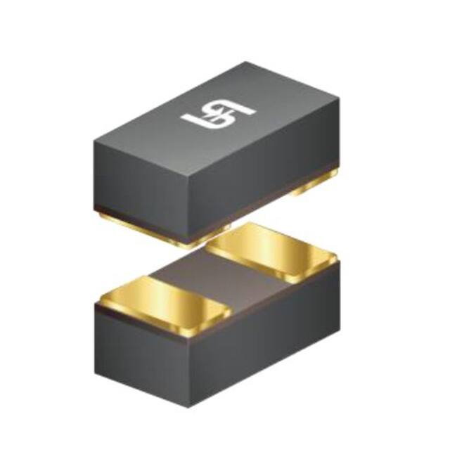
Package
0603
Configuration
Single die
MECHANICAL DATA
●
●
●
●
Case: 0603
Terminal: Gold plated, solderable per MIL-STD-750, method 2026
Polarity: Indicated by cathode band
Weight: 3.00mg (approximately)
0603
ABSOLUTE MAXIMUM RATINGS (TA = 25°C unless otherwise noted)
PARAMETER
SYMBOL
VALUE
UNIT
Power dissipation
PD
150
mW
Forward Voltage @ IF = 10mA
Surge peak forward current, 8.3ms single half
sine-wave superimposed on rated
Junction temperature range
VF
0.9
V
IFSM
2
A
TJ
-55 to +125
°C
Storage temperature range
TSTG
-55 to +125
°C
1
Version: G2009
�TSZU52C2V0 – TSZU52C39
Taiwan Semiconductor
ELECTRICAL SPECIFICATIONS (TA = 25°C unless otherwise noted)
ZENER
VOLTAGE
PART
NUMBER
MARKING
CODE
TSZU52C2V0
Z0
1.90
TSZU52C2V2
Z1
TSZU52C2V4
VZ @ IZ
V
Min
Max
TEST
CURRENT
Operating
Resistance
Rising Operating
Resistance
LEAKAGE CURRENT
IZ
mA
ZZT@ IZT
Ω
Max
IZT
mA
ZZT@ IZK
Ω
Max
IZK
mA
IR@ VR
µA
Max
VR
V
2.10
5
100
5
600
1
100
1.0
2.09
2.31
5
100
5
600
1
100
1.0
Z2
2.28
2.52
5
85
5
600
1
100
1.0
TSZU52C2V7
Z3
2.57
2.84
5
83
5
500
1
75
1.0
TSZU52C3V0
Z4
2.85
3.15
5
95
5
500
1
50
1.0
TSZU52C3V3
Z5
3.14
3.47
5
95
5
500
1
25
1.0
TSZU52C3V6
Z6
3.42
3.78
5
95
5
500
1
15
1.0
TSZU52C3V9
Z7
3.71
4.10
5
95
5
500
1
10
1.0
TSZU52C4V3
Z8
4.09
4.52
5
95
5
500
1
5.0
1.0
TSZU52C4V7
Z9
4.47
4.94
5
78
5
500
1
5.0
2.0
TSZU52C5V1
ZA
4.85
5.36
5
60
5
480
1
0.1
0.8
TSZU52C5V6
ZB
5.32
5.88
5
40
5
400
1
0.1
1.0
TSZU52C6V2
ZC
5.89
6.51
5
10
5
200
1
0.1
2.0
TSZU52C6V8
ZE
6.46
7.14
5
8
5
150
1
0.1
3.0
TSZU52C7V5
ZF
7.13
7.88
5
7
5
50
1
0.1
5.0
TSZU52C8V2
ZG
7.79
8.61
5
7
5
50
1
0.1
6.0
TSZU52C9V1
ZH
8.65
9.56
5
10
5
50
1
0.1
7.0
TSZU52C10
ZJ
9.50
10.50
5
15
5
70
1
0.1
7.5
TSZU52C11
ZK
10.45
11.55
5
20
5
70
1
0.1
8.5
TSZU52C12
ZM
11.40
12.60
5
20
5
90
1
0.1
9.0
TSZU52C13
ZN
12.35
13.65
5
25
5
110
1
0.1
10
TSZU52C15
ZP
14.25
15.75
5
30
5
110
1
0.1
11
TSZU52C16
ZQ
15.20
16.80
5
40
5
170
1
0.1
12
TSZU52C18
ZR
17.10
18.90
5
50
5
170
1
0.1
14
TSZU52C20
ZS
19.00
21.00
5
50
5
220
1
0.1
15
TSZU52C22
ZT
20.90
23.10
5
55
5
220
1
0.1
17
TSZU52C24
ZU
22.80
25.20
5
80
5
220
1
0.1
18
TSZU52C27
ZV
25.65
28.35
5
80
5
250
1
0.1
20
TSZU52C30
ZW
28.50
31.50
5
80
5
250
1
0.1
23
TSZU52C33
ZX
31.35
34.65
5
80
5
250
1
0.1
25
TSZU52C36
ZY
34.20
37.80
5
90
5
250
1
0.1
27
TSZU52C39
ZZ
37.05
40.95
5
90
5
300
1
0.1
29
ORDERING INFORMATION
ORDERING CODE(1)
PACKAGE
PACKING
TSZU52Cx RGG
0603
4K / 7" Reel
Notes:
1.
"x" defines voltage from 2.0V(TSZU52C2V0) to 39V(TSZU52C39)
2
Version: G2009
�TSZU52C2V0 – TSZU52C39
Taiwan Semiconductor
CHARACTERISTICS CURVES
(TA = 25°C unless otherwise noted)
Fig.1 Temperature Coefficients
Fig.2 Temperature Coefficients
TEMPERATURE COEFFICIENT (MV/°C)
7
100
TEMPERATURE COEFFICIENT (MV/°C)
6
5
4
3
2
1
0
-1
-2
-3
-4
1
2
3
4
5
6
7
8
9
10
11
12
10
20
40
50
ZENER VOLTAGE (V)
Fig.3 Effect of Zener Voltage on Zener Impedance
Fig.4 Typical Forward Voltage
1000
FORWARD CURRENT (mA)
IZ(AC)0.1 IZ(DC)
f =1kHZ
IZ=1mA
100
IZ=5mA
10
IZ=20mA
1
100
TJ=125°C
TJ=75°C
10
TJ=25°C
1
1
10
100
0.4
0.5
0.6
ZENER VOLTAGE (V)
400
10
350
CAPACITANCE (pF)
1
TJ=125°C
0.01
TJ=25°C
0.001
0.0001
0.8
0.9
1
1.1
Fig.6 Typical Capacitance
100
0.1
0.7
FORWARD VOLTAGE (V)
Fig.5 Typical Leakage Current
LEAKAGE CURRENT (mA)
30
ZENER VOLTAGE (V)
1000
DYNAMIC IMPEDANCE (OHM)
10
300
0V Bias
1V Bias
250
200
150
100
50
TJ=-55°C
0
0.00001
0
5
10
15
20
25
30
35
40
1
45
10
100
ZENER VOLTAGE (V)
ZENER VOLTAGE (V)
3
Version: G2009
�TSZU52C2V0 – TSZU52C39
Taiwan Semiconductor
CHARACTERISTICS CURVES
(TA = 25°C unless otherwise not)
Fig.7 Steady State Power Derating
0.1
0
0
25
50
75
100
125
TEMPERATURE (°C)
Fig.8 Zener Breakdown Characteristics
ZENER CURRENT (mA)
11
10
9V1
8V2
7V5
6V8
6V2
5V6
4V7
5V1
4V3
3V6
3V9
2
2V2
2V4
2V7
3
3V3
100
10
1
0.1
0.01
0
1
2
3
4
5
6
7
8
9
10
11
12
VZ - ZENER VOLTAGE (V)
Fig.9 Zener Breakdown Characteristics
39
36
33
30
27
24
22
20
18
16
15
13
12
100
ZENER CURRENT (mA)
POWER DISSIPATION (W)
0.2
10
1
0.1
0.01
10
100
VZ - ZENER VOLTAGE (V)
4
Version: G2009
�TSZU52C2V0 – TSZU52C39
Taiwan Semiconductor
PACKAGE OUTLINE DIMENSION
0603
SUGGESTED PAD LAYOUT
5
Version: G2009
�TSZU52C2V0 – TSZU52C39
Taiwan Semiconductor
Notice
Specifications of the products displayed herein are subject to change without notice. TSC or anyone on its behalf,
assumes no responsibility or liability for any errors or inaccuracies.
Purchasers are solely responsible for the choice, selection, and use of TSC products and TSC assumes no liability
for application assistance or the design of Purchasers’ products.
Information contained herein is intended to provide a product description only. No license, express or implied, to
any intellectual property rights is granted by this document. Except as provided in TSC’s terms and conditions of
sale for such products, TSC assumes no liability whatsoever, and disclaims any express or implied warranty,
relating to sale and/or use of TSC products including liability or warranties relating to fitness for a particular purpose,
merchantability, or infringement of any patent, copyright, or other intellectual property right.
The products shown herein are not designed for use in medical, life-saving, or life-sustaining applications.
Customers using or selling these products for use in such applications do so at their own risk and agree to fully
indemnify TSC for any damages resulting from such improper use or sale.
6
Version: G2009
�
很抱歉,暂时无法提供与“TSZU52C2V0 RGG”相匹配的价格&库存,您可以联系我们找货
免费人工找货