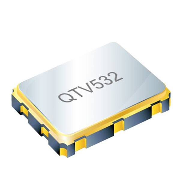
QTV532
Voltage Controlled Crystal Oscillator
Fuel The Digital World
Features
●
●
●
●
●
●
●
●
●
Applications
Frequency range : 1.25MHz to 170MHz
SMD seam sealing ceramic package
Supply voltage : 3.3V
CMOS output
Fundamental solution
Low phase noise and phase jitter
Tri-state function available
External dimensions (mm)
L : 5.0 x W : 3.2 x H : 1.2
RoHS compliant & Pb free
●
●
●
●
●
●
Wireless communications,
Smallcell, Base station
Fibre channel, SONET, SDH,
Ethernet
Set-top box (STB)
xDSL, VoIP, Cable modem
Digital TV, Digital audio
Phase-locked loop (PLL) circuits
Electrical Characteristics
Item
Frequency Range (F0)
Operating Temperature Range (T OTR)
QTV532
1.25MHz ~ 170MHz
-40°C ~ +85°C
-40°C ~ +105°C
Supply Voltage (VDD)
Current Consumption (IDD)
3.3 V
CMOS
Output Load (CL)
15 pF
Output Voltage High (VOH)
90% VDD Min.
Output Voltage Low (VOL)
10% VDD Max.
Rise & Fall Time (Tr / Tf)
5 ns Max.
Duty Cycle
45% ~ 55%
Start-up Time
10 ms Max.
Enable Voltage High, Logic "1"
70% VDD Min.
Enable Voltage Low, Logic "0"
30% VDD Max.
Absolute Pulling Range (APR)
±50 ppm Min.
Control Voltage Range
0V ~ 3.3V
Linearity
10% Max.
Phase Noise (F0 = 122.88MHz)
-128 dBc/Hz Typ.
Phase Jitter (F0 = 122.88MHz)
50 fs Typ.
Rev. 1.01
VDD ± 10%
30 mA Max.
Output Type
Storage Temperature Range (TSTR)
Conditions
10% ~ 90% of output swing
Input to Pin2
Note [1]
Note [2]
Nominal 1.65V
at 1kHz offset
12kHz ~ 20MHz, RMS
-55°C ~ +125°C
Page 1
www.qstproducts.com
�QTV532
Voltage Controlled Crystal Oscillator
Fuel The Digital World
Notes:
[1] Output will be enabled if Pin2 is Logic "1" or open; Output will be disabled if Pin2 is Logic "0".
[2] Absolute Pulling Range (APR) = Pulling Range - (Frequency tolerance at 25°C, variations over
temerature, supply voltage, and aging).
Dimensions
Pin function
Pin 1
VC
Pin 2
OE
Pin 3
GND
Pin 4
OUT
Pin 5
NC
Pin 6
VDD
Recommended pad layout
(Unit: mm)
* Pad dimension tolerance is ±0.2mm
* Power supply decoupling capacitor is required.
Ordering Information
QTV532
-
122.88M B B
Frequency in Hz
-
T
Packaging Method
T
Please contact us for
available frequencies
Tape & Reel
Operating Temperature Range
Supply Voltage
B
Rev. 1.01
B
G
3.3 V
Page 2
-40°C ~ +85°C (APR ± 50 ppm)
-40°C ~ +105°C (APR ± 50 ppm)
www.qstproducts.com
�QTV532
Voltage Controlled Crystal Oscillator
Fuel The Digital World
Packing
(Unit: mm)
Reflow Profile
Solder melting point : 220°C ± 10°C, 60 sec. Min., 200 sec. Max.
Peak temperature : 260°C ± 10°C, 10 sec. Min., 30 sec. Max.
(°C)
10 sec
260
220
180
150
120 sec
Rev. 1.01
60 sec
Page 3
Time (sec)
www.qstproducts.com
�
QTV532-122.880MBG-T 价格&库存
很抱歉,暂时无法提供与“QTV532-122.880MBG-T”相匹配的价格&库存,您可以联系我们找货
免费人工找货