GA10SICP12-247
Silicon Carbide Junction
Transistor/Schottky Diode Co-pack
Features
VDS
RDS(ON)
ID (Tc = 25°C)
hFE (Tc = 25°C)
=
=
=
1200 V
120 m
25 A
100
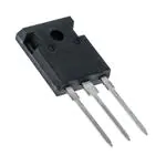
Package
175°C Maximum Operating Temperature
Gate Oxide free SiC switch
Exceptional Safe Operating Area
Integrated SiC Schottky Rectifier
Excellent Gain Linearity
Temperature Independent Switching Performance
Low output capacitance
Positive temperature co-efficient of RDS,ON
Suitable for connecting an anti-parallel diode
RoHS Compliant
D
G D S
TO-247AB
Advantages
Applications
Compatible with Si MOSFET/IGBT Gate Drive ICs
> 20 µs Short-Circuit Withstand Capability
Lowest-in-class Conduction Losses
High Circuit Efficiency
Minimal Input Signal distortion
High Amplifier Bandwidth
Reduced cooling requirements
Reduced system size
Down Hole Oil Drilling, Geothermal Instrumentation
Hybrid Electric Vehicles (HEV)
Solar Inverters
Switched-Mode Power Supply (SMPS)
Power Factor Correction (PFC)
Induction Heating
Uninterruptible Power Supply (UPS)
Motor Drives
Maximum Ratings at Tj = 175 °C, unless otherwise specified
Parameter
Symbol
Conditions
Values
Unit
VDS
ID
IGM
VGS = 0 V
TC,MAX = 95 °C
1200
10
10
ID,max = 10
@ VDS VDSmax
V
A
A
20
µs
30
25
91
-55 to 175
V
V
W
°C
A
A
A
SiC Junction Transistor
Drain Source Voltage
Continuous Drain Current
Gate Peak Current
Turn-Off Safe Operating Area
RBSOA
Short Circuit Safe Operating Area
SCSOA
Reverse Gate Source Voltage
Reverse Drain Source Voltage
Power Dissipation
Storage Temperature
V SG
VSD
Ptot
Tstg
TVJ = 175 oC, IG = 1 A,
Clamped Inductive Load
TVJ = 175 oC, IG = 1 A, VDS = 800 V,
Non Repetitive
TC = 95 °C
A
Free-wheeling Silicon Carbide diode
DC-Forward Current
Non Repetitive Peak Forward Current
Surge Non Repetitive Forward Current
IF
I FM
TC 150 ºC
TC = 25 ºC, tP = 10 s
IF,SM
tP = 10 ms, half sine, TC = 25 ºC
10
280
65
RthJC
RthJC
SiC Junction Transistor
SiC Diode
0.88
0.85
°C/W
°C/W
0.6
Nm
Thermal Characteristics
Thermal resistance, junction - case
Thermal resistance, junction - case
Mechanical Properties
Mounting torque
Aug 2014
M
http://www.genesicsemi.com/commercial-sic/sic-modules-copack/
Pg1 of 8
�GA10SICP12-247
Electrical Characteristics at Tj = 175 °C, unless otherwise specified
Parameter
Symbol
Conditions
min.
Values
typ.
max.
Unit
SJT On-State Characteristics
Drain Source On Resistance
RDS(ON)
Gate Forward Voltage
VGS(FWD)
DC Current Gain
hFE
VDS = 5 V, ID = 10 A, Tj = 25 °C
VDS = 5 V, ID = 10 A, Tj = 175 °C
120
150
220
3.3
3.1
100
TBD
350
530
700
20
nA
tbd
tbd
pF
pF
tbd
tbd
tbd
tbd
tbd
tbd
tbd
tbd
tbd
tbd
tbd
tbd
tbd
tbd
ns
ns
ns
ns
µJ
µJ
µJ
ns
ns
ns
µJ
µJ
µJ
1.55
V
0.8
tbd
tbd
tbd
tbd
tbd
tbd
tbd
tbd
tbd
tbd
tbd
tbd
V
A
ns
ns
ns
J
J
nC
ns
ns
J
J
nC
ID = 10 A, IG = 200 mA, Tj = 25 °C
ID = 10 A, IG = 400 mA, Tj = 125 °C
ID = 10 A, IG = 800 mA, Tj = 175 °C
IG = 500 mA, Tj = 25 °C
IG = 500 mA, Tj = 175 °C
m
V
SJT Off-State Characteristics
Drain Leakage Current
IDSS
Gate Leakage Current
ISG
VR = 1200 V, VGS = 0 V, Tj = 25 °C
VR = 1200 V, V GS = 0 V, Tj = 125 °C
VR = 1200 V, V GS = 0 V, Tj = 175 °C
VSG = 20 V, Tj = 25 °C
Ciss
Crss/Coss
VGS = 0 V, V D = 1 V, f = 1 MHz
VD = 1 V, f = 1 MHz
nA
SJT Capacitance Characteristics
Input Capacitance
Reverse Transfer/Output Capacitance
SJT Switching Characteristics
Turn On Delay Time
Rise Time
Turn Off Delay Time
Fall Time
Turn-On Energy Per Pulse
Turn-Off Energy Per Pulse
Total Switching Energy
Turn On Delay Time
Rise Time
Turn Off Delay Time
Fall Time
Turn-On Energy Per Pulse
Turn-Off Energy Per Pulse
Total Switching Energy
td(on)
tr
td(off)
tf
Eon
Eoff
Ets
td(on)
tr
td(off)
tf
Eon
Eoff
Ets
VDD = 800 V, ID = 10 A,
RG(on) = RG(off) = tbd ,
FWD = GB10SLT12,
Tj = 25 ºC
Refer to Figure 15 for gate current
waveform
VDD = 800 V, ID = 10 A,
RG(on) = RG(off) = tbd ,
FWD = GB10SLT12,
Tj = 175 ºC
Refer to Figure 15 for gate current
waveform
Free-wheeling Silicon Carbide Schottky Diode
Forward Voltage
Diode Knee Voltage
Peak Reverse Recovery Current
Reverse Recovery Time
Rise Time
Fall Time
Turn-On Energy Loss Per Pulse
Turn-Off Energy Loss Per Pulse
Reverse Recovery Charge
Rise Time
Fall Time
Turn-On Energy Loss Per Pulse
Turn-Off Energy Loss Per Pulse
Reverse Recovery Charge
Aug 2014
VF
VD(knee)
Irrm
trr
tr
tf
Eon
Eoff
Qrr
tr
tf
Eon
Eoff
Qrr
IF = 10 A, VGE = 0 V,
Tj = 25 ºC (175 ºC )
Tj = 25 ºC, IF = 1 mA
IF = 10 A, VGE = 0 V, VR = 800 V,
-dI F/dt = 625 A/µs, Tj = 175 ºC
VDD= 800 V, ID = 10 A,
Rgon = Rgoff = tbd ,
Tj= 25 ºC
VDD= 800 V, ID = 10 A,
Rgon = Rgoff = tbd ,
Tj= 175 ºC
http://www.genesicsemi.com/commercial-sic/sic-modules-copack/
Pg2 of 8
�GA10SICP12-247
Figures
TBD
Figure 1: Typical Output Characteristics at 25 °C
TBD
Figure 3: Typical Output Characteristics at 175 °C
TBD
Figure 5: Normalized On-Resistance and Current Gain vs.
Temperature
Aug 2014
TBD
Figure 2: Typical Output Characteristics at 125 °C
TBD
Figure 4: Typical Gate Source I-V Characteristics vs.
Temperature
TBD
Figure 6: Typical Blocking Characteristics
http://www.genesicsemi.com/commercial-sic/sic-modules-copack/
Pg3 of 8
�GA10SICP12-247
TBD
Figure 7: Capacitance Characteristics
TBD
Figure 9: Typical Hard-switched Turn On Waveforms
TBD
Figure 11: Typical Turn On Energy Losses and Switching
Times vs. Temperature
Aug 2014
TBD
Figure 8: Capacitance Characteristics
TBD
Figure 10: Typical Hard-switched Turn Off Waveforms
TBD
Figure 12: Typical Turn Off Energy Losses and Switching
Times vs. Temperature
http://www.genesicsemi.com/commercial-sic/sic-modules-copack/
Pg4 of 8
�GA10SICP12-247
TBD
Figure 13: Typical Turn On Energy Losses vs. Drain
Current
TBD
Figure 15: Typical Gate Current Waveform
TBD
Figure 17: Power Derating Curve
1
TBD
Figure 14: Typical Turn Off Energy Losses vs. Drain
Current
TBD
Figure 16: Typical Hard Switched Device Power Loss vs.
1
Switching Frequency
TBD
Figure 18: Forward Bias Safe Operating Area
Representative values based on device switching energy loss. Actual losses will depend on gate drive conditions, device load, and circuit topology.
Aug 2014
http://www.genesicsemi.com/commercial-sic/sic-modules-copack/
Pg5 of 8
�GA10SICP12-247
TBD
Figure 19: Turn-Off Safe Operating Area
TBD
Figure 20: Transient Thermal Impedance
Figure 21: Typical FWD Forward Characteristics
Aug 2014
http://www.genesicsemi.com/commercial-sic/sic-modules-copack/
Pg6 of 8
�GA10SICP12-247
Gate Drive Theory of Operation for the GA10SICP12-263
The SJT transistor is a current controlled transistor which requires a positive gate current for turn-on as well as to remain in on-state. An ideal
gate current waveform for ultra-fast switching of the SJT, while maintaining low gate drive losses, is shown in Figure 22.
Figure 22: Idealized Gate Current Waveform
Gate Currents, IG,pk/-IG,pk and Voltages during Turn-On and Turn-Off
An SJT is rapidly switched from its blocking state to on-state, when the necessary gate charge, Q G, for turn-on is supplied by a burst of high
gate current, IG,on, until the gate-source capacitance, CGS, and gate-drain capacitance, CGD, are fully charged.
The IG,pon pulse should ideally terminate, when the drain voltage falls to its on-state value, in order to avoid unnecessary drive losses during
the steady on-state. In practice, the rise time of the IG,on pulse is affected by the parasitic inductances, Lpar in the module and drive circuit. A
voltage developed across the parasitic inductance in the source path, Ls, can de-bias the gate-source junction, when high drain currents begin
to flow through the device. The applied gate voltage should be maintained high enough, above the VGS,ON level to counter these effects.
A high negative peak current, -IG,off is recommended at the start of the turn-off transition, in order to rapidly sweep out the injected carriers from
the gate, and achieve rapid turn-off. While satisfactory turn off can be achieved with VGS = 0 V, a negative gate voltage VGS may be used in
order to speed up the turn-off transition.
Steady On-State
After the device is turned on, IG may be advantageously lowered to IG,steady for reducing unnecessary gate drive losses. The IG,steady is
determined by noting the DC current gain, hFE, of the device
The desired IG,steady is determined by the peak device junction temperature TJ during operation, drain current ID, DC current gain hFE, and a
50 % safety margin to ensure operating the device in the saturation region with low on-state voltage drop by the equation:
Aug 2014
http://www.genesicsemi.com/commercial-sic/sic-modules-copack/
Pg7 of 8
�GA10SICP12-247
Package Dimensions:
TO-247AB
PACKAGE OUTLINE
2. DIMENSIONS DO NOT INCLUDE END FLASH, MOLD FLASH, MATERIAL PROTRUSIONS
Revision History
Date
2014/08/25
Revision
1
Comments
Gate Drive Theory Update
2013/09/12
0
Initial release
Supersedes
Published by
GeneSiC Semiconductor, Inc.
43670 Trade Center Place Suite 155
Dulles, VA 20166
GeneSiC Semiconductor, Inc. reserves right to make changes to the product specifications and data in this document without notice.
GeneSiC disclaims all and any warranty and liability arising out of use or application of any product. No license, express or implied to any
intellectual property rights is granted by this document.
Unless otherwise expressly indicated, GeneSiC products are not designed, tested or authorized for use in life-saving, medical, aircraft
navigation, communication, air traffic control and weapons systems, nor in applications where their failure may result in death, personal
injury and/or property damage.
Aug 2014
http://www.genesicsemi.com/commercial-sic/sic-modules-copack/
Pg8 of 8
�