GA06JT12-247
Normally – OFF Silicon Carbide
Junction Transistor
VDS
VDS(ON)
ID
RDS(ON)
Features
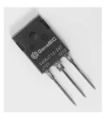
Package
RoHS Compliant
175 °C maximum operating temperature
Temperature independent switching performance
Gate oxide free SiC switch
Suitable for connecting an anti-parallel diode
Positive temperature coefficient for easy paralleling
Low gate charge
Low intrinsic capacitance
=
=
=
=
D
1200 V
1.3 V
6A
220 mΩ
D
G
D
G
S
S
TO-247AB
Applications
Advantages
Low switching losses
Higher efficiency
High temperature operation
High short circuit withstand capability
Down Hole Oil Drilling, Geothermal Instrumentation
Hybrid Electric Vehicles (HEV)
Solar Inverters
Switched-Mode Power Supply (SMPS)
Power Factor Correction (PFC)
Induction Heating
Uninterruptible Power Supply (UPS)
Motor Drives
Maximum Ratings unless otherwise specified
Parameter
Drain – Source Voltage
Continuous Drain Current
Gate Peak Current
Symbol
VDS
ID
IGM
Turn-Off Safe Operating Area
RBSOA
Short Circuit Safe Operating Area
SCSOA
Reverse Gate – Source Voltage
Reverse Drain – Source Voltage
Power Dissipation
Storage Temperature
VSG
VSD
Ptot
Tstg
Conditions
VGS = 0 V
TC,MAX = 90 °C
TVJ = 175 oC, IG = 1 A,
Clamped Inductive Load
TVJ = 175 oC, IG = 1 A, VDS = 800 V,
Non Repetitive
TC = 25 °C
Values
1200
6
5
ID,max = 6
@ VDS ≤ VDSmax
Unit
V
A
A
20
µs
30
40
146
-55 to 175
V
V
W
°C
A
Electrical Characteristics at Tj = 175 °C, unless otherwise specified
Parameter
Symbol
Conditions
min.
Values
typ.
max.
Unit
On Characteristics
Drain – Source On Voltage
VDS(ON)
Drain – Source On Resistance
RDS(ON)
Gate Forward Voltage
VGS(FWD)
DC Current Gain
β
ID = 6 A, IG = 500 mA, Tj = 25 °C
ID = 6 A, IG = 1000 mA, Tj = 125 °C
ID = 6 A, IG = 1000 mA, Tj = 175 °C
ID = 6 A, IG = 500 mA, Tj = 25 °C
ID = 6 A, IG = 1000 mA, Tj = 125 °C
ID = 6 A, IG = 1000 mA, Tj = 175 °C
IG = 500 mA, Tj = 25 °C
IG = 500 mA, Tj = 175 °C
VDS = 5 V, ID = 6 A, Tj = 25 °C
VDS = 5 V, ID = 6 A, Tj = 175 °C
45
1.3
1.7
2.2
220
280
370
3.1
2.9
53
33
1.7
2.2
3.0
0.5
1
2
20
10
50
100
V
mΩ
V
Off Characteristics
Drain Leakage Current
IDSS
Gate Leakage Current
ISG
Nov 2013
VR = 1200 V, VGS = 0 V, Tj = 25 °C
VR = 1200 V, VGS = 0 V, Tj = 125 °C
VR = 1200 V, VGS = 0 V, Tj = 175 °C
VSG = 20 V, Tj = 25 °C
http://www.genesicsemi.com/index.php/sic-products/sjt
µA
nA
Pg1 of 7
�GA06JT12-247
Electrical Characteristics at Tj = 175 °C, unless otherwise specified
Parameter
Symbol
Conditions
Cgs
Ciss
Crss/Coss
VGS = 0 V, f = 1 MHz
VGS = 0 V, VD = 1 V, f = 1 MHz
VD = 1 V, f = 1 MHz
min.
Values
typ.
max.
Unit
Capacitance Characteristics
Gate-Source Capacitance
Input Capacitance
Reverse Transfer/Output Capacitance
660
900
240
pF
pF
pF
13
7
54
51
175
44
219
11
8
79
45
159
55
214
ns
ns
ns
ns
µJ
µJ
µJ
ns
ns
ns
ns
µJ
µJ
µJ
1.03
°C/W
Switching Characteristics
Turn On Delay Time
Rise Time, Drain Current
Turn Off Delay Time
Fall Time, Drain Current
Turn-On Energy Per Pulse
Turn-Off Energy Per Pulse
Total Switching Energy
Turn On Delay Time
Rise Time, Drain Current
Turn Off Delay Time
Fall Time, Drain Current
Turn-On Energy Per Pulse
Turn-Off Energy Per Pulse
Total Switching Energy
td(on)
tr
td(off)
tf
Eon
Eoff
Ets
td(on)
tr
td(off)
tf
Eon
Eoff
Ets
Tj = 25 ºC, VDD = 800 V, ID = 6 A,
“Option #1” Gate Drive
RG(on) = RG(off) = 1.5 Ω, CG = 9 nF
VGH = 20 V, VGL = 6 V, VEE = -5 V
L = 1.05 mH, FWD = GB05SLT12,
Refer to Figure 15 for gate current
waveform
Tj = 175 ºC, VDD = 800 V, ID = 6 A,
“Option #1” Gate Drive
RG(on) = RG(off) = 1.5 Ω, CG = 9 nF
VGH = 20 V, VGL = 6 V, VEE = -5 V
L = 1.05 mH, FWD = GB05SLT12,
Refer to Figure 15 for gate current
waveform
Thermal Characteristics
Thermal resistance, junction - case
RthJC
Figures
Figure 1: Typical Output Characteristics at 25 °C
Nov 2013
Figure 2: Typical Output Characteristics at 125 °C
http://www.genesicsemi.com/index.php/sic-products/sjt
Pg2 of 7
�GA06JT12-247
Figure 3: Typical Output Characteristics at 175 °C
Figure 4: Typical Gate Source I-V Characteristics vs.
Temperature
Figure 5: Normalized On-Resistance and Current Gain vs.
Temperature
Figure 6: Typical Blocking Characteristics
Figure 7: Capacitance Characteristics
Figure 8: Capacitance Characteristics
Nov 2013
http://www.genesicsemi.com/index.php/sic-products/sjt
Pg3 of 7
�GA06JT12-247
Figure 9: Typical Hard-switched Turn On Waveforms
Figure 10: Typical Hard-switched Turn Off Waveforms
Figure 11: Typical Turn On Energy Losses and Switching
Times vs. Temperature
Figure 12: Typical Turn Off Energy Losses and Switching
Times vs. Temperature
Figure 13: Typical Turn On Energy Losses vs. Drain
Current
Figure 14: Typical Turn Off Energy Losses vs. Drain
Current
Nov 2013
http://www.genesicsemi.com/index.php/sic-products/sjt
Pg4 of 7
�GA06JT12-247
1
Figure 15: Typical Gate Current Waveform
Figure 16: Typical Hard Switched Device Power Loss vs.
1
Switching Frequency
Figure 17: Power Derating Curve
Figure 18: Forward Bias Safe Operating Area
Figure 19: Turn-Off Safe Operating Area
Figure 20: Transient Thermal Impedance
– Representative values based on device switching energy loss. Actual losses will depend on gate drive conditions, device load, and circuit topology.
Nov 2013
http://www.genesicsemi.com/index.php/sic-products/sjt
Pg5 of 7
�GA06JT12-247
Gate Drive Technique (Option #1)
To drive the GA06JT12-247 with the lowest gate drive losses, please refer to the dual voltage source gate drive configuration
described in Application Note AN-10B (http://www.genesicsemi.com/index.php/references/notes).
Gate Drive Technique (Option #2)
The GA06JT12-247 can be effectively driven using the IXYS IXDN614 / IXDD614 non-inverting gate driver IC or a comparable
product. A typical gate driver configuration along with component values using this driver is offered below. Additional
information is available in GeneSiC Application Note AN-10A and from the manufacturer at www.ixys.com.
Figure 21: Gate Diver Configuration (Option #2)
Parameter
Symbol
Conditions
min.
Values
typ.
max.
Unit
Option #1 Gate Drive Conditions (IXDD614/IXDN614)
Supply Voltage, High Side Driver
Supply Voltage, Low Side Driver
Off State Voltage, Both Drivers
Gate Control Input Signal, Low
Gate Control Input Signal, High
Enable, Low
Enable, High
Output Voltage, Low
Output Voltage, High
Output Current, Peak
Output Current, Continuous
VCC
VCC
GND
IN
IN
EN
EN
VOUT
VOUT
IOUT
IOUT
15
5
VGH
VGL
VEE
-5.0
4
IXDD614 Only
IXDD614 Only
20
6
-5
0
5.0
30
0
0.8
VCC+0.3
1/3*VCC
2/3*VCC
0.025
VCC-0.025
Package Limited
0.5
14
4.0
V
V
V
V
V
V
V
V
V
A
A
Passive Gate Components
Gate Resistance
Gate Capacitance
Nov 2013
RG
CG
VGL = 6.0 V, IG ≈ 0.5 A
VGH = 20 V, IG,pk ≈ 2.0 A
http://www.genesicsemi.com/index.php/sic-products/sjt
5
1.6
9
5
Ω
nF
Pg6 of 7
�GA06JT12-247
Package Dimensions:
TO-247AB
PACKAGE OUTLINE
NOTE
1. CONTROLLED DIMENSION IS INCH. DIMENSION IN BRACKET IS MILLIMETER.
2. DIMENSIONS DO NOT INCLUDE END FLASH, MOLD FLASH, MATERIAL PROTRUSIONS
Revision History
Date
Revision
Comments
2013/11/13
4
Updated Electrical Characteristics
2013/08/23
3
Updated Switching Characteristics
2013/06/24
2
Updated Electrical Characteristics
2013/02/21
1
Revised Electrical Characteristics
2012/11/30
0
Initial Release
Supersedes
Published by
GeneSiC Semiconductor, Inc.
43670 Trade Center Place Suite 155
Dulles, VA 20166
GeneSiC Semiconductor, Inc. reserves right to make changes to the product specifications and data in this document without notice.
GeneSiC disclaims all and any warranty and liability arising out of use or application of any product. No license, express or implied to any
intellectual property rights is granted by this document.
Unless otherwise expressly indicated, GeneSiC products are not designed, tested or authorized for use in life-saving, medical, aircraft
navigation, communication, air traffic control and weapons systems, nor in applications where their failure may result in death, personal
injury and/or property damage.
Nov 2013
http://www.genesicsemi.com/index.php/sic-products/sjt
Pg7 of 7
�GA06JT12-247
SPICE Model Parameters
Copy the following code into a SPICE software program for simulation of the GA06JT12 SJT device.
*
MODEL OF GeneSiC Semiconductor Inc.
*
*
$Revision:
1.0
$
*
$Date:
26-AUG-2013
$
*
*
GeneSiC Semiconductor Inc.
*
43670 Trade Center Place Ste. 155
*
Dulles, VA 20166
*
http://www.genesicsemi.com/index.php/sic-products/sjt
*
*
COPYRIGHT (C) 2013 GeneSiC Semiconductor Inc.
*
ALL RIGHTS RESERVED
*
* These models are provided "AS IS, WHERE IS, AND WITH NO WARRANTY
* OF ANY KIND EITHER EXPRESSED OR IMPLIED, INCLUDING BUT NOT LIMITED
* TO ANY IMPLIED WARRANTIES OF MERCHANTABILITY AND FITNESS FOR A
* PARTICULAR PURPOSE."
* Models accurate up to 2 times rated drain current.
*
.model GA06JT12 NPN
+ IS
5.08E-47
+ ISE
1.26E-28
+ EG
3.2
+ BF
58.31
+ BR
0.55
+ IKF
200
+ NF
1
+ NE
1.892
+ RB
0.26
+ RE
0.1039
+ RC
0.06188
+ CJC
2.73E-10
+ VJC
3.04
+ MJC
0.448
+ CJE
6.86E-10
+ VJE
2.89
+ MJE
0.466
+ XTI
3
+ XTB
-1.33
+ TRC1
1.90E-2
+ VCEO
1200
+ ICRATING 6
+ MFG
GeneSiC_Semiconductor
*
* End of GA06JT12 SPICE Model
Aug 2013
http://www.genesicsemi.com/index.php/sic-products/sjt
Pg1 of 1
�