GA50JT06-258
Normally – OFF Silicon Carbide
Junction Transistor
Features
Package
210°C maximum operating temperature
Gate Oxide Free SiC Switch
Exceptional Safe Operating Area
Excellent Gain Linearity
Compatible with 5 V TTL Gate Drive
Temperature Independent Switching Performance
Low Output Capacitance
Positive Temperature Coefficient of RDS,ON
Suitable for Connecting an Anti-parallel Diode
VDS
=
600 V
RDS(ON)
=
25 m
ID
(Tc = 25°C)
=
100 A
hFE (Tc = 25°C)
=
105
D
D
G
G
D
S
S
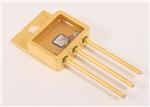
TO-258
Advantages
Applications
Compatible with Si MOSFET/IGBT Gate Drive ICs
> 20 µs Short-Circuit Withstand Capability
Lowest-in-class Conduction Losses
High Circuit Efficiency
Minimal Input Signal Distortion
High Amplifier Bandwidth
Down Hole Oil Drilling
Geothermal Instrumentation
Solenoid Actuators
General Purpose High-Temperature Switching
Amplifiers
Solar Inverters
Switched-Mode Power Supply (SMPS)
Power Factor Correction (PFC)
Table of Contents
Section I: Absolute Maximum Ratings ...........................................................................................................1
Section II: Static Electrical Characteristics....................................................................................................2
Section III: Dynamic Electrical Characteristics .............................................................................................2
Section IV: Figures ...........................................................................................................................................3
Section V: Driving the GA50JT06-247.............................................................................................................7
Section VI: Package Dimensions ................................................................................................................. 10
Section VII: SPICE Model Parameters ......................................................................................................... 11
Section I: Absolute Maximum Ratings
Parameter
Drain – Source Voltage
Continuous Drain Current
Continuous Gate Current
Symbol
VDS
ID
IGM
Turn-Off Safe Operating Area
RBSOA
Short Circuit Safe Operating Area
SCSOA
Reverse Gate – Source Voltage
Reverse Drain – Source Voltage
Power Dissipation
Operating and Storage Temperature
Dec 2014
VSG
VSD
Ptot
Tstg
Conditions
VGS = 0 V
TJ = 210°C, TC = 25°C
TJ = 210°C, IG = 3.5 A,
Clamped Inductive Load
TJ = 210°C, IG = 3.5 A, VDS = 400 V,
Non Repetitive
TJ = 210°C, TC = 25°C
Value
600
100
3.5
ID,max = 50
@ VDS
DSmax
Unit
V
A
A
Notes
A
Fig. 18
>20
µs
30
25
769
-55 to 210
V
V
W
°C
http://www.genesicsemi.com/high-temperature-sic/high-temperature-sic-junction-transistors/
Fig. 16
Pg1 of 10
�GA50JT06-258
Section II: Static Electrical Characteristics
Parameter
Symbol
Conditions
Min.
Value
Typical
Max.
Unit
Notes
A: On State
Drain – Source On Resistance
RDS(ON)
ID = 50 A, Tj = 25 °C
ID = 50 A, Tj = 125 °C
ID = 50 A, Tj = 175 °C
ID = 50 A, Tj = 210 °C
Gate – Source Saturation Voltage
VGS,SAT
ID = 50 A, ID/IG = 40, Tj = 25 °C
ID = 50 A, ID/IG = 30, Tj = 175 °C
hFE
VDS = 5 V,
VDS = 5 V,
VDS = 5 V,
VDS = 5 V,
Drain Leakage Current
IDSS
VR = 600 V, VGS = 0 V, Tj = 25 °C
VR = 600 V, VGS = 0 V, Tj = 125 °C
VR = 600 V, VGS = 0 V, Tj = 210 °C
Gate Leakage Current
ISG
VSG = 20 V, Tj = 25 °C
DC Current Gain
25
39
43
50
3.42
3.23
105
77
71
70
ID = 50 A, Tj = 25 °C
ID = 50 A, Tj = 125 °C
ID = 50 A, Tj = 175 °C
ID = 50 A, Tj = 210 °C
Fig. 5
V
Fig. 7
–
Fig. 5
A
Fig. 8
B: Off State
10
50
100
20
nA
0.26
°C/W
Fig. 19
Unit
Notes
6450
420
17.4
pF
pF
µJ
Fig. 9
Fig. 9
Fig. 10
C: Thermal
Thermal resistance, junction - case
RthJC
Section III: Dynamic Electrical Characteristics
Parameter
Symbol
Conditions
Min.
Value
Typical
Max.
A: Capacitance and Gate Charge
Input Capacitance
Reverse Transfer/Output Capacitance
Output Capacitance Stored Energy
Effective Output Capacitance,
time related
Effective Output Capacitance,
energy related
Gate-Source Charge
Gate-Drain Charge
Gate Charge - Total
B: Switching
VGS = 0 V, VD = 100 V, f = 1 MHz
VD = 100 V, f = 1 MHz
VGS = 0 V, VD = 400 V, f = 1 MHz
Coss,tr
ID = constant, VGS = 0 V, VDS = 0…400 V
390
pF
Coss,er
VGS = 0 V, VDS = 0…400 V
284
pF
QGS
QGD
QG
VGS = -5…3 V
VGS = 0 V, VDS = 0…400 V
55
156
211
nC
nC
nC
1
Internal Gate Resistance – zero bias
Internal Gate Resistance – ON
Turn On Delay Time
Fall Time, VDS
Turn Off Delay Time
Rise Time, VDS
Turn On Delay Time
Fall Time, VDS
Turn Off Delay Time
Rise Time, VDS
Turn-On Energy Per Pulse
Turn-Off Energy Per Pulse
Total Switching Energy
Turn-On Energy Per Pulse
Turn-Off Energy Per Pulse
Total Switching Energy
1
Ciss
Crss/Coss
EOSS
f = 1 MHz, V
= 50 mV, V
= 0 V,
DS
RG(INT-ZERO) V = 0 V, T AC
GS
j = 210 ºC
RG(INT-ON) VGS > 2.5 V, VDS = 0 V, Tj = 210 ºC
td(on)
Tj = 25 ºC, VDS = 400 V,
tf
ID = 50 A, Resistive Load
Refer to Section V for additional
td(off)
driving information.
tr
td(on)
tf
Tj = 210 ºC, VDS = 400 V,
ID = 50 A, Resistive Load
td(off)
tr
Eon
Tj = 25 ºC, VDS = 400 V,
ID = 50 A, Inductive Load
Eoff
Refer to Section V.
Etot
Eon
Tj = 210 ºC, VDS = 400 V,
Eoff
ID = 50 A, Inductive Load
Etot
0.9
0.09
25
44
40
33
19
43
89
27
690
359
1049
758
337
1095
ns
ns
ns
ns
ns
ns
ns
ns
µJ
µJ
µJ
µJ
µJ
µJ
Fig. 11,13
Fig. 12,14
Fig. 11
Fig. 12
Fig. 11,13
Fig. 12,14
Fig. 11
Fig. 12
– All times are relative to the Drain-Source Voltage VDS
Dec 2014
http://www.genesicsemi.com/high-temperature-sic/high-temperature-sic-junction-transistors/
Pg2 of 10
�GA50JT06-258
Section IV: Figures
A: Static Characteristics
Figure 1: Typical Output Characteristics at 25 °C
Figure 2: Typical Output Characteristics at 125 °C
Figure 3: Typical Output Characteristics at 210 °C
Figure 4: Drain-Source Voltage vs. Gate Current
Figure 5: Normalized On-Resistance and Current Gain vs.
Temperature
Dec 2014
Figure 6: DC Current Gain vs. Drain Current
http://www.genesicsemi.com/high-temperature-sic/high-temperature-sic-junction-transistors/
Pg3 of 10
�GA50JT06-258
Figure 7: Typical Gate – Source Saturation Voltage
Figure 8: Typical Blocking Characteristics
B: Dynamic Characteristics
Figure 9: Input, Output, and Reverse Transfer Capacitance
Figure 10: Output Capacitance Stored Energy
Figure 11: Typical Turn On Energy Losses and Switching
Times vs. Temperature
Figure 12: Typical Turn Off Energy Losses and Switching
Times vs. Temperature
Dec 2014
http://www.genesicsemi.com/high-temperature-sic/high-temperature-sic-junction-transistors/
Pg4 of 10
�GA50JT06-258
2
Figure 13: Typical Turn On Energy Losses and Switching
Times vs. Drain Current
Figure 14: Typical Turn Off Energy Losses and Switching
Times vs. Drain Current
Figure 15: Typical Hard Switched Device Power Loss vs.
Switching Frequency 2
Figure 16: Power Derating Curve
Figure 17: : Forward Bias Safe Operating Area at Tc= 25 oC
Figure 18: Turn-Off Safe Operating Area
– Representative values based on device conduction and switching loss. Actual losses will depend on gate drive conditions, device load, and circuit topology.
Dec 2014
http://www.genesicsemi.com/high-temperature-sic/high-temperature-sic-junction-transistors/
Pg5 of 10
�GA50JT06-258
Figure 19: Transient Thermal Impedance
Dec 2014
Figure 20: Drain Current Derating vs. Pulse Width
http://www.genesicsemi.com/high-temperature-sic/high-temperature-sic-junction-transistors/
Pg6 of 10
�GA50JT06-258
Section V: Driving the GA50JT06-247
The GA50JT06-247 is a current controlled SiC transistor which requires a positive gate current for turn-on and to remain in on-state. It may be
driven by different drive topologies depending on the intended application.
Table 1: Estimated Power Consumption and switching frequencies for various Gate Drive topologies.
Gate Drive Power
Switching
Drive Topology
Consumption
Frequency
Simple TTL
High
Low
Constant Current
Medium
Medium
High Speed – Boost Capacitor
Medium
High
High Speed – Boost Inductor
Low
High
Proportional
Lowest
Medium
Pulsed Power
Medium
N/A
A: Simple TTL Drive
The GA50JT06-247 may be driven by 5 V TTL logic by using a simple current amplification stage. The current amplifier output current must
meet or exceed the steady state gate current, IG,steady, required to operate the GA50JT06-247. An external gate resistor RG, shown in the
Figure 21 topology, sets IG,steady to the required level which is dependent on the SJT drain current I D and DC current gain hFE, RG may be
calculated from the equation below. The values of hFE and VGS,sat may be read from Figure 6 and Figure 7, respectively. VEC,sat can be taken
from the PNP datasheet, a partial list of high-temperature PNP and NPN transistors options is given below. High-temperature MOSFETs may
also be used in the topology.
,
=
5.0
,
Inverting
Current
Boost
Stage
(
)
,
1.5
(
SiC SJT
G
IG,steady
0/5V
TTL i/p
inverted
)
5V
PNP
TTL
Gate Signal
( ,
)
0/5V
TTL o/p
RG
NPN
D
S
Figure 21: Simple TTL Gate Drive Topology
Table 2: Partial List of High-Temperature BJTs for TTL Gate Driving
Dec 2014
BJT Part Number
Type
Tj,max (°C)
PHPT60603PY
PHPT60603NY
2N2222
2N6730
2N2905
2N5883
2N5885
PNP
NPN
NPN
PNP
PNP
PNP
NPN
175
175
200
200
200
200
200
http://www.genesicsemi.com/high-temperature-sic/high-temperature-sic-junction-transistors/
Pg7 of 10
�GA50JT06-258
B: High Speed Driving
For ultra high speed GA50JT06-247 switching (tr, tf < 20 ns) while maintaining low gate drive losses the supplied gate current should include a
positive current peak during turn-on, a negative voltage peak during turn-off, and continuous gate current IG to remain on.
An SJT is rapidly switched from its blocking state to on-state, when the necessary gate charge for turn-on, QG, is supplied by a burst of high
gate current until the gate-source capacitance, CGS, and gate-drain capacitance, CGD, are fully charged. Ideally, the burst should terminate
when the drain voltage has fallen to its on-state value in order to avoid unnecessary drive losses. A negative voltage peak is recommended for
the turn-off transition in order to ensure that the gate current is not being supplied under high dV/dt due to the Miller effect. While satisfactory
turn off can be achieved with VGS = 0 V, a negative VGS value may be used in order to speed up the turn-off transition.
B:1: High Speed, Low Loss Drive with Boost Capacitor
The GA50JT06-247 may be driven using a High Speed, Low Loss Drive with Boost Capacitor topology in which multiple voltage levels, a gate
resistor, and a gate capacitor are used to provide current peaks at turn-on and turn-off for fast switching and a continuous gate current while in
on-state. As shown in Figure 22, in this topology two gate driver ICs are utilized. An external gate resistor RG is driven by a low voltage driver
to supply the continuous gate current throughout on-state.and a gate capacitor CG is driven at a higher voltage level to supply a high current
peak at turn-on and turn-off. A 3 kV isolated evaluation gate drive board (GA03IDDJT30-FR4) from GeneSiC Semiconductor utilizing this
topology is commercially available for high and low-side driving, its datasheet provides additional details about this drive topology.
VGH
CG
Gate Signal
IG G
VGL
Gate
SiC SJT
RG
D
S
Figure 22: High Speed, Low Loss Drive with Boost Capacitor Topology
B:2: High Speed, Low Loss Drive with Boost Inductor
A High Speed, Low-Loss Driver with Boost Inductor is also capable of driving the GA50JT06-247 at high-speed. It utilizes a gate drive inductor
instead of a capacitor to provide the high-current gate current pulses IG,on and IG,off. During operation, inductor L is charged to a specified I G,on
current value then made to discharge IL into the SJT gate pin using logic control of S1, S2, S3, and S4, as shown in Figure 23. After turn on,
while the device remains on the necessary steady state gate current I G,steady is supplied from source VCC through RG. Please refer to the article
“A current-source concept for
driving topology.3
VCC
S1
VCC
S2
L
S3
S4
VEE
SiC SJT
G
RG
D
S
VEE
Figure 23: High Speed, Low-Loss Driver with Boost Inductor Topology
3
– Archives of Electrical Engineering. Volume 62, Issue 2, Pages 333–343, ISSN (Print) 0004-0746, DOI: 10.2478/aee-2013-0026, June 2013
Dec 2014
http://www.genesicsemi.com/high-temperature-sic/high-temperature-sic-junction-transistors/
Pg8 of 10
�GA50JT06-258
C: Proportional Gate Current Driving
A proportional gate drive topology may be beneficial for applications in which the GA50JT06-247 will operate over a wide range of drain
current conditions to lower the gate drive power consumption. A proportional gate driver relies on instantaneous drain current I D feedback to
vary the steady state gate current IG,steady supplied to the GA50JT06-247.
C:1: Voltage Controlled Proportional Driver
A voltage controlled proportional driver relies on a gate drive integrated circuit to detect the GA50JT06-247 drain-source voltage V DS during
on-state to sense ID. The integrated circuit will then increase or decrease IG in response to ID. This allows IG and gate drive power consumption
to reduce while ID is low or for IG to increase when ID increases. A high voltage diode connected between the drain and sense protects the
integrated circuit from high-voltage when blocking. A simplified version of this topology is shown in Figure 24. Additional information will be
available in the future at http://www.genesicsemi.com/references/product-notes/.
HV Diode
Sense
Gate Signal
Proportional
Gate Current
Driver
Signal
G
Output
D
IG,steady
SiC SJT
S
Figure 24: Simplified Voltage Controlled Proportional Driver
C:2: Current Controlled Proportional Driver
The current controlled proportional driver relies on a low-loss transformer in the drain or source path to provide feedback of the
GA50JT06-247 drain current during on-state to supply IG,steady into the gate. IG,steady will increase or decrease in response to ID at a fixed forced
current gain which is set be the turns ratio of the transformer, hforce = ID / IG = N2 / N1. GA50JT06-247 is initially tuned-on using a gate current
pulse supplied into an RC drive circuit to allow ID current to begin flowing. This topology allows IG,steady and the gate drive power consumption to
reduce while ID is relatively low or for IG,steady to increase when ID increases. A simplified version of this topology is shown in Figure 25.
Additional information will be available in the future at http://www.genesicsemi.com/references/product-notes/.
N2
SiC SJT
Gate Signal
G
D
S
N3
N1
N2
Figure 25: Simplified Current Controlled Proportional Driver
Dec 2014
http://www.genesicsemi.com/high-temperature-sic/high-temperature-sic-junction-transistors/
Pg9 of 10
�GA50JT06-258
Section VI: Package Dimensions
TO-258
PACKAGE OUTLINE
NOTE
1. CONTROLLED DIMENSION IS INCH. DIMENSION IN BRACKET IS MILLIMETER.
2. DIMENSIONS DO NOT INCLUDE END FLASH, MOLD FLASH, MATERIAL PROTRUSIONS
Revision History
Date
Revision
2014/12/12
2014/08/23
2014/04/10
5
4
3
Updated Electrical Characteristics
Updated Electrical Characteristics
Updated Electrical Characteristics
Comments
2014/02/05
2013/12/19
2
1
Updated Electrical Characteristics
Updated Gate Drive Section
2013/12/05
0
Initial release
Supersedes
Published by
GeneSiC Semiconductor, Inc.
43670 Trade Center Place Suite 155
Dulles, VA 20166
GeneSiC Semiconductor, Inc. reserves right to make changes to the product specifications and data in this document without notice.
GeneSiC disclaims all and any warranty and liability arising out of use or application of any product. No license, express or implied to any
intellectual property rights is granted by this document.
Unless otherwise expressly indicated, GeneSiC products are not designed, tested or authorized for use in life-saving, medical, aircraft
navigation, communication, air traffic control and weapons systems, nor in applications where their failure may result in death, personal
injury and/or property damage.
Dec 2014
http://www.genesicsemi.com/high-temperature-sic/high-temperature-sic-junction-transistors/
Pg10 of 10
�GA50JT06-258
Section VII: SPICE Model Parameters
This is a secure document. Please copy this code from the SPICE model PDF file on our website
(http://www.genesicsemi.com/images/hit_sic/sjt/GA50JT06-258_SPICE.pdf) into LTSPICE (version 4)
software for simulation of the GA50JT06-258.
*
MODEL OF GeneSiC Semiconductor Inc.
*
*
$Revision:
1.3
$
*
$Date:
12-DEC-2014
$
*
*
GeneSiC Semiconductor Inc.
*
43670 Trade Center Place Ste. 155
*
Dulles, VA 20166
*
*
COPYRIGHT (C) 2014 GeneSiC Semiconductor Inc.
*
ALL RIGHTS RESERVED
*
* These models are provided "AS IS, WHERE IS, AND WITH NO WARRANTY
* OF ANY KIND EITHER EXPRESSED OR IMPLIED, INCLUDING BUT NOT LIMITED
* TO ANY IMPLIED WARRANTIES OF MERCHANTABILITY AND FITNESS FOR A
* PARTICULAR PURPOSE."
* Models accurate up to 2 times rated drain current.
*
.model GA50JT06 NPN
*
+ IS
5.00E-47
+ ISE
1.26E-26
+ EG
3.23
+ BF
106
+ BR
0.55
+ IKF
9000
+ NF
1
+ NE
2
+ RB
0.9
+ IRB
0.002
+ RBM
0.09
+ RE
0.01
+ RC
0.013
+ CJC
2.3989E-9
+ VJC
2.8346223
+ MJC
0.4846
+ CJE
6.026E-09
+ VJE
3.17915435
+ MJE
0.52951635
+ XTI
3
+ XTB
-1.2
+ TRC1
7.00E-3
+ VCEO
600
+ ICRATING 100
+ MFG
GeneSiC_Semiconductor
*
* End of GA50JT06 SPICE Model
Dec 2014
http://www.genesicsemi.com/commercial-sic/sic-junction-transistors/
Pg1 of 1
�


 工商网监
湘ICP备2023018690号
工商网监
湘ICP备2023018690号