Advanced Science And Novel Technology Company, Inc.
2790 Skypark Drive Suite 112, Torrance, CA 90505
Offices: 310-530-9400 / Fax: 310-530-9402
www.adsantec.com
ASNT7113A-KHC
4.0GSps / 20GHz Differential Track-and-Hold Amplifier
gaincrl
vcc
varcrl
vcc
vp0p9
More than 8-bit accuracy within the full frequency range
Sampling speed from 50MSps to 4GSps
Nominal 0dB differential gain with manual adjustment
Adjustable duty cycle of the internal sampling clocks
Adjustable input bandwidth
Adjustable overall gain
Fully differential input and output data and clock buffers with on-chip 50Ohm termination
Dual power supply
Total power consumption of 1.75W
Fabricated in SiGe for high performance, yield, and reliability
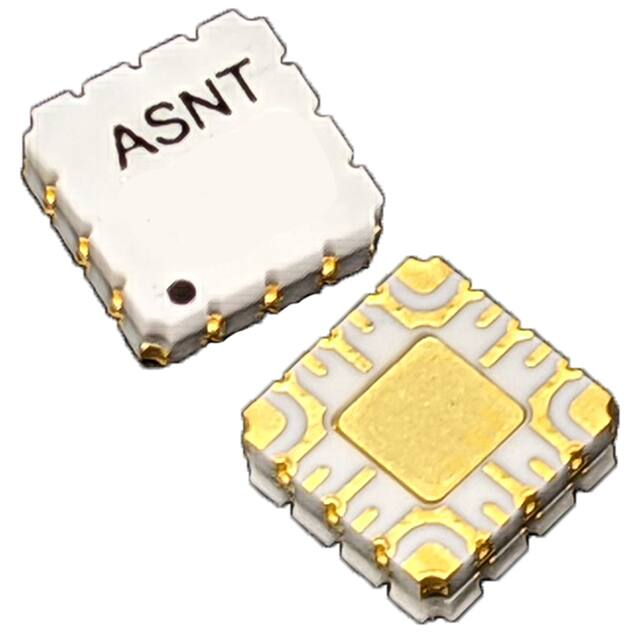
Custom CQFN 24-pin package
vcc
vee
vcc
vcc
dp
qp
vcc
vcc
1
vcc
cn
vcc
vcc
vcc
cp
qn
vcc
dn
t2crl
Rev. 1.0.2
ASNT7113A
vee
March 2021
�Advanced Science And Novel Technology Company, Inc.
2790 Skypark Drive Suite 112, Torrance, CA 90505
Offices: 310-530-9400 / Fax: 310-530-9402
www.adsantec.com
DESCRIPTION
vp0p9 varcrl
dp
dn
cp
cn
Input
Data
Equalizer
Sampling
Strobe
Generator
data
Sampling
Output
Block
Buffer
qp
qn
s1
s2
t2crl
gaincrl
Fig. 1. Functional Block Diagram
The ASNT7113A-KHC SiGe IC is a high-speed, temperature stable, and broadband track-and-hold
amplifier (THA) with improved reliability. The IC shown in Fig. 1 performs sampling of an input
differential analog signal using two internally-generated strobe signals s1 and s2, and delivers a step-like
differential signal to the output. It features an adjustable track period length controlled by the t2crl voltage
that modifies the states of internal delay lines. This allows for maximizing the length of the valid output
step.
The differential gain of the chip is approximately 0dB, which corresponds to a single-ended-to-differential
gain of -6dB. The gain can be adjusted using the external control voltage gaincrl. The chip supports both
AC-coupled, and DC-coupled inputs. In the DC-coupled mode, the input common-mode voltage must be
equal to vcc for optimal performance of the chip. The input sampled data path includes an equalizer that
increases the bandwidth of the chip. The level of equalization is controlled by the external voltage varcrl.
The frequency response, and gain of the part is also controlled by the positive supply voltage vp0p9 that
powers the input buffers of the Track-and-Hold. This voltage defines the common mode of the data signal
at the input of the sampling switch, and thus the frequency response of the device. Lower voltages result
in less peaking in the input buffer, and less overall gain of the device.
The part’s outputs support the CML-type logic interface with an on-chip 50Ohm termination to vcc, and
may be used differentially, AC/DC coupled, single-ended, or in any combination (also see POWER
SUPPLY CONFIGURATION). The differential DC signaling mode is recommended for optimal
performance.
Rev. 1.0.2
2
March 2021
�Advanced Science And Novel Technology Company, Inc.
2790 Skypark Drive Suite 112, Torrance, CA 90505
Offices: 310-530-9400 / Fax: 310-530-9402
www.adsantec.com
Input Data Equalizer
The input data’s bandwidth can be adjusted by the internal equalizer controlled with the external voltage
varcrl. The equalizer is designed to compensate for the gain drop at high frequencies due to the
characteristics of the front-end circuitry, and the sampling block itself. The measured frequency response
of the IC at maximum (magenta line) and minimum (orange line) values of the varcrl voltage is shown in
Fig. 2. The measurements have been performed at the intermediate setting of the gain control (see Fig. 4).
1
0
Gain, dB
-1
-2
-3
-4
-5
0.1
1
VarMAX
10
100
F, GHz
VarMIN
Fig. 2. Frequency Response of SHA with Max and Min Equalization
Input Clock Buffer
The input clock buffer converts an external clock cp/cn into two internal signals s1 and s2 with
controlled pulse width (PW) as shown in Fig. 3.
Track
Hold
s2
s1
PW
Valid output
Fig. 3. Sampling Diagram
This allows for optimization of the hold time, and the length of the valid output signal period. The value
of PW is reversely proportional to the t2crl voltage.
Sampling Block with Output Buffer
The sampling block performs conversion of the input signal into a step-like sampled signal under control
of s1 and s2 pulses. The sampled signal is amplified by the output buffer to achieve a total gain of
approximately 0dB. The gain can be adjusted using the gaincrl voltage signal. The measured frequency
response of the SHA with the maximum and minimum gain at 2.5GSps rate is shown in Fig. 4.
Rev. 1.0.2
3
March 2021
�Advanced Science And Novel Technology Company, Inc.
2790 Skypark Drive Suite 112, Torrance, CA 90505
Offices: 310-530-9400 / Fax: 310-530-9402
www.adsantec.com
1
0
Gain, dB
-1
-2
-3
-4
-5
-6
0.1
1
10
100
F, GHz
Fig. 4. THA Gain at Max and Min gaincrl Values vs. Data Frequency
The harmonic distortion of the THA has been demonstrated by its 3rd harmonic as shown in Fig. 5 for
differential clock, and data input signals at the sampling rate of 4GSps. The data amplitude is 125mV
differential or 125mV pk-pk at both direct and inverted pins.
-5 0
-5 1
-5 2
-5 3
dBc
-5 4
-5 5
-5 6
-5 7
-5 8
-5 9
-6 0
0
2
4
6
8
10
12
14
16
18
20
Fdata, GHz
Fig. 5. 3-rd Harmonic at 4GHz Input Clock (C) and 125mV Differential Data (D) Amplitude
The linearity of the signal conversion is illustrated by Fig. 6 that demonstrates the part’s gain at 2.5GSps.
-0.86
-0.88
-0.9
Gain, dB
-0.92
-0.94
-0.96
-0.98
-1
-1.02
-1.04
-1.06
0
50
100
150
200
250
300
InputAmplitude SE, mV p-p
Fig. 6. THA Gain vs. Input Data Amplitude at Medium State of gaincrl
Rev. 1.0.2
4
March 2021
�Advanced Science And Novel Technology Company, Inc.
2790 Skypark Drive Suite 112, Torrance, CA 90505
Offices: 310-530-9400 / Fax: 310-530-9402
www.adsantec.com
POWER SUPPLY CONFIGURATION
The part operates with either a negative supply scheme (vcc = 0.0V = ground), or a positive supply
scheme (vee = 0V = ground). In case of the positive supply, all I/Os need AC termination when
connected to any devices with 50Ohm termination to ground. Different PCB layouts will be needed for
each different power supply combination.
ABSOLUTE MAXIMUM RATINGS
Caution: Exceeding the absolute maximum ratings shown in Table 1 may cause damage to this product
and/or lead to reduced reliability. Functional performance is specified over the recommended operating
conditions for power supply and temperature only. AC and DC device characteristics at or beyond the
absolute maximum ratings are not assumed or implied.
Table 1. Absolute Maximum Ratings
Parameter
Min
Max
Units
First Supply Voltage (vee)
-3.5 (negative scheme) 0 (positive scheme)
V
Second Supply Voltage (vcc)
0 (negative scheme) 3.5 (positive scheme)
V
Third Supply Voltage (vp0p9)
vcc+1.1
V
Power Consumption
2
W
RF Input Voltage Swing (Diff)
2.0
V pk-pk
Clock Input Voltage Swing (Diff)
1.0
V pk-pk
Case Temperature
+90
ºC
Storage Temperature
-40
+100
ºC
Operational and storage Humidity
10
98
%
TERMINAL FUNCTIONS
TERMINAL
Name
No.
Type
DESCRIPTION
High-Speed I/Os
Sampling clock inputs with internal SE 50Ohm termination to
vcc
Analog
Analog sampled data inputs with internal SE 50Ohm
input
termination to vcc
CML output Differential data outputs with internal SE 50Ohm termination
to vcc. Require external SE 50Ohm termination to vcc
Controls
t2crl
1
Analog voltage Sampling clock delay control
gaincrl
13 Analog voltage Gain adjustment
varcrl
15 Analog voltage Equalizer peaking control
Supply and Termination Voltages
Name
Description
Pin Number
st
vcc
1 positive supply voltage
2, 4, 6, 8, 10, 12, 14, 16, 18, 20, 22, 24
vee
Negative power supply
7, 19
nd
vp0p9 2 positive power supply
17
cp
cn
dp
dn
qp
qn
Rev. 1.0.2
3
5
21
23
11
9
CML input
5
March 2021
�Advanced Science And Novel Technology Company, Inc.
2790 Skypark Drive Suite 112, Torrance, CA 90505
Offices: 310-530-9400 / Fax: 310-530-9402
www.adsantec.com
ELECTRICAL CHARACTERISTICS
PARAMETER
MAX
UNIT
COMMENTS
General Parameters
-3.3 / 0
-3.2 / 0
-3.1 / 0
V
Negative scheme / Positive scheme
vee
0 / 3.1
0 / 3.2
0 / 3.3
V
Negative scheme / Positive scheme
vcc
0.75
0.85
0.95
V
Above vcc, any scheme
vp0p9
Ivcc
430
mA
Ivee = Ivcc + Ivp0p9
Ivp0p9
100
mA
Power consumption
1750
mW
Junction temperature
-25
50
125
°C
Input Data (dp/dn)
Input data frequency
0.0
20
GHz
Swing, differential,
0
300
mV
3rd HD