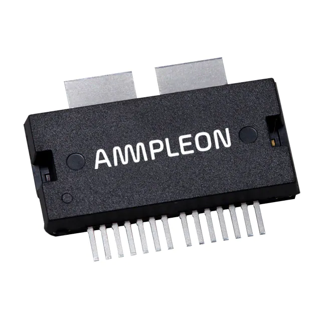
BLM7G22S-60PB;
BLM7G22S-60PBG
LDMOS 2-stage power MMIC
Rev. 5 — 1 September 2015
Product data sheet
1. Product profile
1.1 General description
The BLM7G22S-60PB(G) is a dual path, 2-stage power MMIC using Ampleon’s state of
the art GEN7 LDMOS technology. This device is perfectly suited as general purpose
driver in the frequency range from 2100 MHz to 2400 MHz. Available in gull wing or flat
lead outline.
Table 1.
Application performance
Typical RF performance at Tcase = 25 C; IDq1 = 75 mA; IDq2 = 233 mA.
Test signal: 3GPP test model 1; 64 DPCH; clipping at 46 %; PAR = 8.4 dB at 0.01% probability on
CCDF per carrier; carrier spacing = 5 MHz; per section unless otherwise specified in a class-AB
production circuit.
f
VDS
PL(AV)
Gp
D
ACPR
(MHz)
(V)
(W)
(dB)
(%)
(dBc)
2-carrier W-CDMA
2140
28
1.6
31.5
11.3
43
2-carrier W-CDMA
2350
28
1.6
29.3
10.7
42
Test signal
1.2 Features and benefits
Integrated temperature compensated bias
Biasing of individual stages is externally accessible
Integrated current sense
Integrated ESD protection
Excellent thermal stability
High power gain
On-chip matching for ease of use (input matched to 50 ; output partially matched)
Designed for broadband operation (frequency 2100 MHz to 2400 MHz)
Compliant to Directive 2002/95/EC, regarding restriction of hazardous substances
(RoHS)
1.3 Applications
RF power MMIC for W-CDMA base stations in the 2100 MHz to 2400 MHz frequency
range.
�BLM7G22S-60PB(G)
LDMOS 2-stage power MMIC
2. Pinning information
2.1 Pinning
pin 1 index
VDS(A1)
VGSS(A2)
VDSS(A2)
RF_IN_A
VGSS(A1)
VDSS(A1)
n.c.
n.c.
VDSS(B1)
VGSS(B1)
RF_IN_B
VDSS(B2)
VGSS(B2)
VDS(B1)
1
2
3
4
5
6
7
16
RF_OUT_A / VDS(A2)
8
9
10
11
12
13
14
15
RF_OUT_B / VDS(B2)
aaa-004384
Transparent top view
The exposed backside of the package is the ground terminal of the device.
Fig 1.
Pin configuration
2.2 Pin description
Table 2.
BLM7G22S-60PB_7G22S-60PBG#5
Product data sheet
Pin description
Symbol
Pin
Description
VDS(A1)
1
drain-source voltage of stage A1
VGSS(A2)
2
gate sense FET and gate source voltage of stage A2
VDSS(A2)
3
drain sense FET source voltage of stage A2
RF_IN_A
4
RF input path A
VGSS(A1)
5
gate sense FET and gate source voltage of stage A1
VDSS(A1)
6
drain sense FET source voltage of stage A1
n.c.
7
not connected
n.c.
8
not connected
VDSS(B1)
9
drain sense FET source voltage of stage B1
VGSS(B1)
10
gate sense FET and gate source voltage of stage B1
RF_IN_B
11
RF input path of B
VDSS(B2)
12
drain sense FET source voltage of stage B2
VGSS(B2)
13
gate sense FET and gate source voltage of stage B2
VDS(B1)
14
drain-source voltage of stage B1
All information provided in this document is subject to legal disclaimers.
Rev. 5 — 1 September 2015
© Ampleon The Netherlands B.V. 2015. All rights reserved.
2 of 21
�BLM7G22S-60PB(G)
LDMOS 2-stage power MMIC
Table 2.
Pin description …continued
Symbol
Pin
Description
RF_OUT_B/VDS(B2)
15
RF output path B / drain source voltage of stage B2
RF_OUT_A/VDS(A2)
16
RF output path A / drain source voltage of stage A2
GND
flange RF ground
3. Ordering information
Table 3.
Ordering information
Type number
Package
Name
Description
Version
BLM7G22S-60PB
HSOP16F
plastic, heatsink small outline package; 16 leads (flat)
SOT1211-2
BLM7G22S-60PBG
HSOP16
plastic, heatsink small outline package; 16 leads
SOT1212-2
4. Block diagram
VDS(A1)
RF_IN_A
RF_OUT_A / VDS(A2)
VGSS(A1)
VDSS(A1)
VGSS(A2)
VDSS(A2)
TEMPERATURE
COMPENSATED BIAS
VGSS(B2)
VDSS(B2)
VGSS(B1)
VDSS(B1)
TEMPERATURE
COMPENSATED BIAS
RF_IN_B
RF_OUT_B / VDS(B2)
VDS(B1)
aaa-004385
Fig 2.
Block diagram of BLM7G22-60PBG
5. Limiting values
Table 4.
Limiting values
In accordance with the Absolute Maximum Rating System (IEC 60134).
Symbol
Parameter
VDS
Min
Max
Unit
drain-source voltage
-
65
V
VGS
gate-source voltage
0.5
+13
V
VGS(sense)
sense gate-source voltage
0.5
+9
V
Tstg
storage temperature
65
+150
C
-
225
C
-
150
C
Tj
junction temperature
Tcase
case temperature
[1]
BLM7G22S-60PB_7G22S-60PBG#5
Product data sheet
Conditions
[1]
Continuous use at maximum temperature will affect the reliability, for details refer to the on-line MTF
calculator.
All information provided in this document is subject to legal disclaimers.
Rev. 5 — 1 September 2015
© Ampleon The Netherlands B.V. 2015. All rights reserved.
3 of 21
�BLM7G22S-60PB(G)
LDMOS 2-stage power MMIC
6. Thermal characteristics
Table 5.
Thermal characteristics
Measured for total device.
Symbol Parameter
Rth(j-c)
[1]
Conditions
thermal resistance from
junction to case
Value Unit
final stage; Tcase = 90 C; PL = 3.2 W
[1]
1.1
K/W
driver stage; Tcase = 90 C; PL = 3.2 W
[1]
3.2
K/W
When operated with a CW signal.
7. Characteristics
Table 6.
DC characteristics
Tcase = 25 C; per section unless otherwise specified.
Symbol
Parameter
Conditions
Min Typ
Max Unit
Final stage
V(BR)DSS
drain-source breakdown voltage VGS = 0 V; ID = 0.422 mA
65
-
-
V
VGS(th)
gate-source threshold voltage
VDS = 10 V; ID = 42 mA
1.4
1.9
2.4
V
VGSq
gate-source quiescent voltage
VDS = 28 V; ID = 253 mA
1.7
2.1
2.5
V
IDSS
drain leakage current
VGS = 0 V; VDS = 28 V
-
-
1.4
A
IDSX
drain cut-off current
VGS = VGS(th) + 3.75 V;
VDS = 10 V
-
7.8
-
A
140
IGSS
gate leakage current
VGS = 11 V; VDS = 0 V
-
-
gfs
forward transconductance
VDS = 10 V; ID = 1478 mA
-
2.85 -
S
RDS(on)
drain-source on-state resistance VGS = VGS(th) + 3.75 V;
ID = 1.48 A
-
350
-
m
IDq
quiescent drain current
208 233
257
mA
main transistor: VDS = 28 V
nA
sense transistor: ID = 7 mA;
VDS = 28 V
Driver stage
V(BR)DSS
drain-source breakdown voltage VGS = 0 V; ID = 0.116 mA
65
-
-
V
VGS(th)
gate-source threshold voltage
VDS = 10 V; ID = 11.6 mA
1.4
1.9
2.4
V
VGSq
gate-source quiescent voltage
VDS = 28 V; ID = 69.6 mA
1.7
2.1
2.5
V
IDSS
drain leakage current
VGS = 0 V; VDS = 28 V
-
-
1.4
A
IDSX
drain cut-off current
VGS = VGS(th) + 3.75 V;
VDS = 10 V
-
2.2
-
A
IGSS
gate leakage current
VGS = 11 V; VDS = 0 V
-
-
140
nA
gfs
forward transconductance
VDS = 10 V; ID = 406 mA
-
0.8
-
RDS(on)
drain-source on-state resistance VGS = VGS(th) + 3.75 V;
ID = 0.4 A
-
2350 -
m
IDq
quiescent drain current
67
75
mA
main transistor: VDS = 28 V
83
S
sense transistor: ID = 7 mA;
VDS = 28 V
BLM7G22S-60PB_7G22S-60PBG#5
Product data sheet
All information provided in this document is subject to legal disclaimers.
Rev. 5 — 1 September 2015
© Ampleon The Netherlands B.V. 2015. All rights reserved.
4 of 21
�BLM7G22S-60PB(G)
LDMOS 2-stage power MMIC
Table 7.
RF Characteristics
Typical RF performance at Tcase = 25 C; VDS = 28 V; IDq1 = 75 mA; IDq2 = 233 mA. Test signal:
2-carrier W-CDMA; 3GPP test model 1; 64 DPCH; clipping at 46 %; PAR = 8.4 dB at 0.01%
probability on CCDF per carrier; carrier spacing = 5 MHz; f = 2140 MHz; per section unless
otherwise specified, measured in a class-AB production circuit.
Symbol
Parameter
Conditions
Min
Typ
Max
Unit
Gp
power gain
PL(AV) = 1.6 W
29.5
31.5
33.5
dB
D
drain efficiency
PL(AV) = 1.6 W
10
11.3
-
%
RLin
input return loss
PL(AV) = 1.6 W
-
17
10
dB
ACPR
adjacent channel power ratio
PL(AV) = 1.6 W
-
43
40
dBc
8. Application information
8.1 Circuit information for application circuit (2.1 GHz to 2.2 GHz)
Table 8.
List of components
For test circuit see Figure 3.
BLM7G22S-60PB_7G22S-60PBG#5
Product data sheet
Component
Description
Value
C1, C4, C21, C24, C100, C200, C300, C400
capacitor
10 F
Remarks
C2, C5, C6, C22, C25, C26
capacitor
1 F
C3, C7, C10, C23, C27, C30
capacitor
8.2 pF
[1]
C8, C28
capacitor
1.6 pF
[1]
C9, C29
capacitor
0.4 pF
[1]
C11, C31
electrolytic capacitor 470 F
C101, C201, C301, C401
capacitor
100 nF
C102, C103, C105, C202, C203, C205,
C302, C303, C305, C402, C403, C405
capacitor
12 pF
C104, C204, C304, C404
capacitor
4.7 F
D100, D200, D300, D400
IC: LM4051
-
P100, P400
potentiometer
-
Q100, Q200, Q300, Q400
IC: LM7341
-
[2]
do not populate
R1, R21
ferrite bead
-
R100, R200, R300, R400
resistor
4.7
R101, R108, R208, R308, R401, R408
resistor
0
R102, R402
resistor
360
1% tolerance
1% tolerance
R103, R403
resistor
330
R104, R203, R303, R404
resistor
68 k
R105, R405
resistor
10 k
R106, R205, R305, R406
resistor
820
R107, R206, R306, R407
resistor
47
R109, R209, R309, R409
resistor
300 k
R201, R301
resistor
180
All information provided in this document is subject to legal disclaimers.
Rev. 5 — 1 September 2015
1% tolerance
© Ampleon The Netherlands B.V. 2015. All rights reserved.
5 of 21
�BLM7G22S-60PB(G)
LDMOS 2-stage power MMIC
Table 8.
List of components …continued
For test circuit see Figure 3.
BLM7G22S-60PB_7G22S-60PBG#5
Product data sheet
Component
Description
Value
Remarks
R202, R302
resistor
3.6 k
1% tolerance
R204, R304
resistor
9.1 k
R207, R307
resistor
1 k
[1]
American Technical Ceramics type 100B or capacitor of same quality.
[2]
American Technical Ceramics type 100A or capacitor of same quality.
All information provided in this document is subject to legal disclaimers.
Rev. 5 — 1 September 2015
© Ampleon The Netherlands B.V. 2015. All rights reserved.
6 of 21
�xxxxxxxxxxxxxxxxxxxxx xxxxxxxxxxxxxxxxxxxxxxxxxx xxxxxxx x x x xxxxxxxxxxxxxxxxxxxxxxxxxxxxxx xxxxxxxxxxxxxxxxxxx xx xx xxxxx
xxxxxxxxxxxxxxxxxxxxxxxxxxx xxxxxxxxxxxxxxxxxxx xxxxxx xxxxxxxxxxxxxxxxxxxxxxxxxxxxxxxxxxx xxxxxxxxxxxx x x
xxxxxxxxxxxxxxxxxxxxx xxxxxxxxxxxxxxxxxxxxxxxxxxxxxx xxxxx xxxxxxxxxxxxxxxxxxxxxxxxxxxxxxxxxxxxxxxxxxxxxxxxxx xxxxxxxx
xxxxxxxxxxxxxxxxxxxxxxxxx xxxxxxxxxxxxxxxxxxxx xxx
BLM7G22S-60PB_7G22S-60PBG#5
Product data sheet
Vbias(A2)
VDS(A1)
R1
Vds-A2
GND
GND
R100
VGSS(A2)
P100
C1
R101
C101
C201 C202
R106
R201
C103
R202
C205
C203
C303
C305
R304 R305
C28
C403
15
R408
R303
14
C301 C302
VDSS(B2)
R406
R410
VGSS(B1)
BLM7G22S-60PBG
2110-2170 MHz
RO4350 / 30 mil
R208
R308
R207 C204 R206
R307 C304 R306
Q300
16
R108
R205
R204
C8
1
Rev. 5 — 1 September 2015
C405
R404
R407
C404
R105
R409
C26
C27
C30
D400 C23
R402
C401
R403
C29
Q400
C24
C402
C22
C31
C25
R401
R400
7 of 21
© Ampleon The Netherlands B.V. 2015. All rights reserved.
C21
GND
GND
R21
Vbias(B2)
VDS(B1)
VGSS(B2)
Printed-Circuit Board (PCB): Rogers 4350; thickness = 0.762 mm.
See Table 8 for a list of components.
Fig 3.
Component layout for class-AB application circuit with auto-bias
Vds-B2
aaa-004523
LDMOS 2-stage power MMIC
P400
BLM7G22S-60PB(G)
All information provided in this document is subject to legal disclaimers.
R107
C105
Q200
R203
C200
VDSS(A1)
GND VDSS(B1)
R309
C300
D300
C400
C10
C104
R104
D200
R301
R302
C9
R105
R110
VGSS(A1)
R300
C11
C7
C6
D100
R209
Vbias(A1)
C4
C3
Q100
VDSS(A2)
Vbias(B1)
C5
R109
R102
C100
R200
C2
C102
R103
�BLM7G22S-60PB(G)
LDMOS 2-stage power MMIC
8.2 Performance curves (2.1 GHz to 2.2 GHz)
Performance curves are measured in a class-AB dedicated application circuit with
auto-bias from 2.1 GHz to 2.2 GHz, see Table 8 and Figure 3.
8.2.1 W-CDMA
aaa-004511
35
15
Gp
(dB)
ηD
(%)
33
13
-42
11
-44
29
9
-46
27
7
-48
31
Gp
ηD
25
2050
2100
2150
2200
f (MHz)
5
2250
-50
2050
Tcase = 25 C; VDS = 28 V; PL(AV) = 1.6 W; IDq1 = 75 mA;
IDq2 = 232 mA; carrier spacing = 5 MHz.
Fig 4.
Power gain and drain efficiency as function of
frequency; typical values
aaa-004513
34
2100
2150
2200
f (MHz)
Fig 5.
Adjacent channel power ratio as a function of
frequency; typical values
aaa-004514
0
ηD
(%)
2250
Tcase = 25 C; VDS = 28 V; PL(AV) = 1.6 W; IDq1 = 75 mA;
IDq2 = 232 mA; carrier spacing = 5 MHz.
40
Gp
(dB)
aaa-004512
-40
ACPR
(dBc)
ACPR
(dBc)
-10
32
30
Gp
-20
30
20
-30
ηD
28
10
-40
26
0
0
2
4
6
8
10
12
PL (W)
-50
14
0
Tcase = 25 C; VDS = 28 V; f = 2140 MHz; IDq1 = 75 mA;
IDq2 = 232 mA; carrier spacing = 5 MHz.
Fig 6.
Power gain and drain efficiency as function of
output power; typical values
BLM7G22S-60PB_7G22S-60PBG#5
Product data sheet
2
4
6
8
10
12
PL (W)
14
Tcase = 25 C; VDS = 28 V; f = 2140 MHz; IDq1 = 75 mA;
IDq2 = 232 mA; carrier spacing = 5 MHz.
Fig 7.
Adjacent channel power ratio as a function of
output power; typical values
All information provided in this document is subject to legal disclaimers.
Rev. 5 — 1 September 2015
© Ampleon The Netherlands B.V. 2015. All rights reserved.
8 of 21
�BLM7G22S-60PB(G)
LDMOS 2-stage power MMIC
aaa-005989
250
IDq
(mA)
aaa-005990
35
Gp
(dB)
IDq2
200
Gp
(1)
ηD
(%)
33
32
(1)
(2)
(3)
(2)
150
31
100
29
40
ηD
24
16
(3)
IDq1
50
27
0
-40
8
25
-20
0
20
40
60
80 100
Tcase (°C)
120
0
0
2
4
6
8
10
PL (W)
12
VDS = 28 V; f = 2140 MHz; IDq1 = 75 mA; IDq2 = 232 mA;
carrier spacing = 5 MHz.
(1) Tcase = 30 C
(2) Tcase = +25 C
(3) Tcase = +100 C
Fig 8.
Quiescent drain current as a function of case
temperature; typical values
Fig 9.
Power gain and drain efficiency as function of
output power; typical values
8.2.2 1-Tone pulsed CW
aaa-005991
32
Gp
(dB)
aaa-005992
35
Gp
(dB)
(1)
31
33
30
31
29
29
(2)
(3)
(3)
28
27
(2)
(1)
27
25
0
5
10
15
20
25
30
35
PL (W)
40
Tcase = 25 C; VDS = 28 V; PL(AV) = 1.6 W; f = 2140 MHz;
IDq1 = 75 mA; IDq2 = 232 mA; = 10 %; tp = 100 s.
0
5
10
(1) Tcase = 30 C
(2) VDD = 28 V
(2) Tcase = +25 C
25
30
35
PL (W)
40
(3) Tcase = +100 C
(3) VDD = 32 V
Fig 10. Power gain as a function of output power;
typical values
Product data sheet
20
VDS = 28 V; PL(AV) = 1.6 W; f = 2140 MHz; IDq1 = 75 mA;
IDq2 = 232 mA; = 10 %; tp = 100 s.
(1) VDD = 24 V
BLM7G22S-60PB_7G22S-60PBG#5
15
Fig 11. Power gain as a function of output power;
typical values
All information provided in this document is subject to legal disclaimers.
Rev. 5 — 1 September 2015
© Ampleon The Netherlands B.V. 2015. All rights reserved.
9 of 21
�BLM7G22S-60PB(G)
LDMOS 2-stage power MMIC
8.2.3 2-Tone CW
aaa-005993
-5
IMD
(dBc)
-25
-45
-65
IMD3
IMD5
IMD7
-85
10-1
1
10
PL(PEP) (W)
102
Tcase = 25 C; VDS = 28 V; fc = 2140 MHz; IDq1 = 75 mA; IDq2 = 232 mA; tone spacing = 100 kHz.
Fig 12. Intermodulation distortion as a function of peak envelope power load power;
typical values
BLM7G22S-60PB_7G22S-60PBG#5
Product data sheet
All information provided in this document is subject to legal disclaimers.
Rev. 5 — 1 September 2015
© Ampleon The Netherlands B.V. 2015. All rights reserved.
10 of 21
�BLM7G22S-60PB(G)
LDMOS 2-stage power MMIC
8.3 Performance curves (2.3 GHz to 2.4 GHz)
Performance curves are measured in a class-AB dedicated application circuit with
auto-bias from 2.3 GHz to 2.4 GHz.
8.3.1 2-Carrier W-CDMA
aaa-014909
31
Gp
(dB)
30.5
aaa-014910
-20
ACPR
(dBc)
-26
30
-32
29.5
-38
(1)
(2)
(3)
29
(1)
(2)
(3)
-44
28.5
28
-50
24
28
32
36
40
44
PL (dBm)
48
VDS = 28 V; IDq1 = 220 mA; IDq2 = 75 mA; carrier
spacing = 5MHz.
24
28.8
(1) f = 2300 MHz
(2) f = 2350 MHz
(2) f = 2350 MHz
(3) f = 2400 MHz
(3) f = 2400 MHz
BLM7G22S-60PB_7G22S-60PBG#5
Product data sheet
38.4
43.2
PL (dBm)
48
VDS = 28 V; IDq1 = 220 mA; IDq2 = 75 mA; carrier
spacing = 5MHz.
(1) f = 2300 MHz
Fig 13. Power gain as a function of output power;
typical values
33.6
Fig 14. Adjacent channel power ratio as a function of
output power; typical values
All information provided in this document is subject to legal disclaimers.
Rev. 5 — 1 September 2015
© Ampleon The Netherlands B.V. 2015. All rights reserved.
11 of 21
�BLM7G22S-60PB(G)
LDMOS 2-stage power MMIC
aaa-014911
35
ηD
(%)
30
25
(3)
(2)
(1)
20
15
10
5
28
32
36
40
44
PL (dBm)
48
VDS = 28 V; IDq1 = 220 mA; IDq2 = 75 mA; carrier spacing = 5MHz.
(1) f = 2300 MHz
(2) f = 2350 MHz
(3) f = 2400 MHz
Fig 15. Drain efficiency as a function of output power; typical values
8.3.2 Pulsed CW
aaa-014912
32
Gp
(dB)
aaa-014913
60
ηD
(%)
31
50
30
40
(1)
(2)
(3)
29
(3)
(2)
(1)
30
28
20
27
10
26
0
24
28
32
36
40
44
PL (dBm)
48
VDS = 28 V; IDq1 = 220 mA; IDq2 = 75 mA; = 10 %;
tp = 100 s.
24
28
(1) f = 2300 MHz
(2) f = 2350 MHz
(2) f = 2350 MHz
(3) f = 2400 MHz
(3) f = 2400 MHz
BLM7G22S-60PB_7G22S-60PBG#5
Product data sheet
36
40
44
PL (dBm)
48
VDS = 28 V; IDq1 = 220 mA; IDq2 = 75 mA; = 10 %;
tp = 100 s.
(1) f = 2300 MHz
Fig 16. Power gain as a function of output power;
typical values
32
Fig 17. Drain efficiency as a function of output power;
typical values
All information provided in this document is subject to legal disclaimers.
Rev. 5 — 1 September 2015
© Ampleon The Netherlands B.V. 2015. All rights reserved.
12 of 21
�BLM7G22S-60PB(G)
LDMOS 2-stage power MMIC
8.4 Application without auto-bias
VDS(A1)
VGSS(A2)
VDSS(A2)
RF_IN_A
VGSS(A1)
VDSS(A1)
n.c.
n.c.
VDSS(B1)
VGSS(B1)
RF_IN_B
VDSS(B2)
VGSS(B2)
VDS(B1)
1
2
3
4
16
RF_OUT_A / VDS(A2)
15
RF_OUT_B / VDS(B2)
5
6
7
8
9
10
11
12
13
14
aaa-004386
Connect pins 2 and 3; connect pins 5 and 6; connect pins 9 and 10; connect pins 12 and 13 at
board level. The exposed backside of the package is the ground terminal of the device.
Fig 18. Non auto-bias application
9. Test information
9.1 Ruggedness
The BLM7G22S-60PB and BLM7G22S-60PBG are capable of withstanding a load
mismatch corresponding to VSWR = 10 : 1 through all phases under the following
conditions: VDS = 28 V; IDq1 = 75 mA; IDq2 = 233 mA; PL = 27 W (W-CDMA);
f = 2140 MHz.
BLM7G22S-60PB_7G22S-60PBG#5
Product data sheet
All information provided in this document is subject to legal disclaimers.
Rev. 5 — 1 September 2015
© Ampleon The Netherlands B.V. 2015. All rights reserved.
13 of 21
�BLM7G22S-60PB(G)
LDMOS 2-stage power MMIC
9.2 Impedance information
Table 9.
Typical impedance
Measured load-pull data. Typical values per section unless otherwise specified.
f
ZS [1]
ZL [1]
(MHz)
()
()
2080
58.86 + j21.82
10.54 j3.20
2110
58.70 + j29.76
10.23 j2.72
2140
51.80 + j41.56
9.56 j2.90
2170
47.31 + j44.60
9.10 j2.80
2230
38.35 + j46.53
8.41 j2.05
2300
30.80 + j53.60
6.40 j2.10
2350
23.80 + j48.20
5.70 j2.20
2400
19.10 + j43.20
5.30 j2.40
55.62 + j18.89
15.89 j2.28
BLM7G22S-60PB
BLM7G22S-60PBG
2080
2110
55.61 + j19.04
14.74 j2.59
2140
55.60 + j19.12
13.56 j2.75
2170
55.57 + j19.25
12.38 j2.75
2200
55.53 + j19.39
11.20 j2.61
2230
55.48 + j19.55
10.05 j2.34
2300
34.51 + j41.45
7.06 j6.36
2350
29.26 + j36.91
6.35 j6.24
2400
22.86 + j32.52
5.65 j6.15
[1]
ZS and ZL defined in Figure 19.
drain
ZL
gate
ZS
001aaf059
Fig 19. Definition of transistor impedance
BLM7G22S-60PB_7G22S-60PBG#5
Product data sheet
All information provided in this document is subject to legal disclaimers.
Rev. 5 — 1 September 2015
© Ampleon The Netherlands B.V. 2015. All rights reserved.
14 of 21
�BLM7G22S-60PB(G)
LDMOS 2-stage power MMIC
9.3 Performance curves
Performance curves are measured per section.
aaa-005994
60
ηD
(%)
48
36
24
12
0
40
42
44
46
48
PL(1dB) (dBm)
50
Tcase = 25 C; VDS = 28 V; PL(AV) = 1.6 W; f = 2140 MHz; IDq1 = 75 mA; IDq2 = 232 mA; = 10 %;
tp = 100 s.
Fig 20. One-tone pulsed CW drain efficiency at 1 dB gain compression as function of
output power at 1 dB gain compression; typical values
BLM7G22S-60PB_7G22S-60PBG#5
Product data sheet
All information provided in this document is subject to legal disclaimers.
Rev. 5 — 1 September 2015
© Ampleon The Netherlands B.V. 2015. All rights reserved.
15 of 21
�BLM7G22S-60PB(G)
LDMOS 2-stage power MMIC
10. Package outline
HSOP16F: plastic, heatsink small outline package; 16 leads(flat)
SOT1211-2
D
E
X
c
D3
E3
B
y
A
HE
v
A
D1
D2
e1
b1(2x)
w
16
B
15
(8x) METAL
PROTRUSIONS (SOURCE)
e6
(2x)
F(16x)
e5
(2x)
E2
A
E1
A2
Q1
pin 1
index
A1
detail X
1
14
b(14x)
e2
w
B
e (12x)
e3 (2x)
HE
e4 (2x)
0
Q1
v
w
y
16.16 1.62
0.1
15.96 1.57 0.25 0.25
15.76 1.52
10 mm
scale
Dimensions (mm are the original dimensions)
Unit
mm
max
nom
min
A
3.9
A1
A2
b
b1
c
D(1)
D1
D2
D3
E(1)
E1
E2
E3
e
e1
e2
0.2 3.65 0.40 5.55 0.27 20.62 19.00 16.05 20.44 10.01 8.18 5.89 9.83
0.1 3.60 0.35 5.50 0.22 20.57 18.95 16.00 20.39 9.96 8.13 5.84 9.78 1.0 7.45 1.5
0 3.55 0.30 5.45 0.17 20.52 18.90 15.95 20.34 9.91 8.08 5.79 9.73
e3
e4
References
IEC
JEDEC
JEITA
e6
F
8.45 9.55 2.97 4.07 0.2
Note
1. Package body dimensions “D and “E do not include mold and metal protrusions. Allowable protrusion is 0.25 mm per side.
2. Lead width dimensions “b and “ b1 do not include dambar protrusions. Allowable dambar protrusion is 0.25 mm in total per lead.
Outline
version
e5
European
projection
sot1211-2_po
Issue date
15-01-12
15-06-09
SOT1211-2
Fig 21. Package outline SOT1211-2 (HSOP16F)
BLM7G22S-60PB_7G22S-60PBG#5
Product data sheet
All information provided in this document is subject to legal disclaimers.
Rev. 5 — 1 September 2015
© Ampleon The Netherlands B.V. 2015. All rights reserved.
16 of 21
�BLM7G22S-60PB(G)
LDMOS 2-stage power MMIC
HSOP16: plastic, heatsink small outline package; 16 leads
SOT1212-2
E
X
E3
A
D
c
B
D3
y
v
HE
A
D1
D2
e1
b1(2x)
w
16
B
(8x) METAL
PROTRUSIONS (SOURCE)
15
e6
e5
(2x)
(2x)
Q
E2
E1
A
A2
(A3)
A1 A4
pin 1 index
θ
1
H
14
Lp
detail X
e2
e
(12x)
b
(14x)
w
B
e3 (2x)
e4 (2x)
HE
0
Unit
mm
max
nom
min
A
3.9
A1
A2
A3
A4
b
b1
c
D(1)
10 mm
D1
D2
D3
E(1)
Q
v
w
y
13.5 1.10 2.07
0.1
13.2 0.95 2.02 0.25 0.25
12.9 0.80 1.97
scale
Dimensions (mm are the original dimensions)
Lp
E1
E2
E3
e
e1
e2
e3
e4
e5
θ
7°
3°
0°
e6
0.2 3.65
0.06 0.40 5.55 0.27 20.62 19.00 16.05 20.44 10.01 8.18 5.89 9.83
0.1 3.60 0.35 0 0.35 5.50 0.22 20.57 18.95 16.00 20.39 9.96 8.13 5.84 9.78 1.0 7.45 1.5 8.45 9.55 2.97 4.07
0 3.55
-0.02 0.30 5.45 0.17 20.52 18.90 15.95 20.34 9.91 8.08 5.79 9.73
Note
1. Package body dimensions “D'' and `'E'' do not include mold and metal protrusions. Allowable protrusion is 0.25 mm per side.
2. Lead width dimensions `'b'' and `'b1'' do not include dambar protrusions. Allowable dambar protrusion is 0.25 mm in total per lead.
3. Dimension A4 is measured with respect to bottom of the heatsink DATUM H. Positive value means that the bottom of the heatsink is
higher than the bottom of the lead.
Outline
version
References
IEC
JEDEC
JEITA
European
projection
sot1212-2_po
Issue date
15-01-14
15-06-09
SOT1212-2
Fig 22. Package outline SOT1212-2 (HSOP16)
BLM7G22S-60PB_7G22S-60PBG#5
Product data sheet
All information provided in this document is subject to legal disclaimers.
Rev. 5 — 1 September 2015
© Ampleon The Netherlands B.V. 2015. All rights reserved.
17 of 21
�BLM7G22S-60PB(G)
LDMOS 2-stage power MMIC
11. Handling information
CAUTION
This device is sensitive to ElectroStatic Discharge (ESD). Observe precautions for handling
electrostatic sensitive devices.
Such precautions are described in the ANSI/ESD S20.20, IEC/ST 61340-5, JESD625-A or
equivalent standards.
12. Abbreviations
Table 10.
Abbreviations
Acronym
Description
3GPP
3rd Generation Partnership Project
CCDF
Complementary Cumulative Distribution Function
CW
Continuous Waveform
DPCH
Dedicated Physical CHannel
ESD
ElectroStatic Discharge
FET
Field-Effect Transistor
GEN7
Seventh Generation
LDMOS
Laterally Diffused Metal Oxide Semiconductor
MMIC
Monolithic Microwave Integrated Circuit
MTF
Median Time To Failure
PAR
Peak-to-Average Ratio
VSWR
Voltage Standing Wave Ratio
W-CDMA
Wideband Code Division Multiple Access
13. Revision history
Table 11.
Revision history
Document ID
Release date
Data sheet status
BLM7G22S-60PB_7G22S-60PBG#5
20150901
Product data sheet
Modifications:
Change notice
Supersedes
BLM7G22S-60PB_
7G22S-60PBG v.4
•
The format of this document has been redesigned to comply with the new
identity guidelines of Ampleon.
•
Legal texts have been adapted to the new company name where
appropriate.
BLM7G22S-60PB_7G22S-60PBG v.4
20150701
Product data sheet
-
BLM7G22S-60PB_
7G22S-60PBG v.3
BLM7G22S-60PB_7G22S-60PBG v.3
20141016
Product data sheet
-
BLM7G22S-60PB_
7G22S-60PBG v.2
BLM7G22S-60PB_7G22S-60PBG v.2
20140930
Product data sheet
-
BLM7G22S-60PB_
7G22S-60PBG v.1
BLM7G22S-60PB_7G22S-60PBG v.1
20121211
Product data sheet
-
-
BLM7G22S-60PB_7G22S-60PBG#5
Product data sheet
All information provided in this document is subject to legal disclaimers.
Rev. 5 — 1 September 2015
© Ampleon The Netherlands B.V. 2015. All rights reserved.
18 of 21
�BLM7G22S-60PB(G)
LDMOS 2-stage power MMIC
14. Legal information
14.1 Data sheet status
Document status[1][2]
Product status[3]
Objective [short] data sheet
Development
This document contains data from the objective specification for product development.
Preliminary [short] data sheet
Qualification
This document contains data from the preliminary specification.
Product [short] data sheet
Production
This document contains the product specification.
Definition
[1]
Please consult the most recently issued document before initiating or completing a design.
[2]
The term ‘short data sheet’ is explained in section “Definitions”.
[3]
The product status of device(s) described in this document may have changed since this document was published and may differ in case of multiple devices. The latest product status
information is available on the Internet at URL http://www.ampleon.com.
14.2 Definitions
Draft — The document is a draft version only. The content is still under
internal review and subject to formal approval, which may result in
modifications or additions. Ampleon does not give any representations or
warranties as to the accuracy or completeness of information included herein
and shall have no liability for the consequences of use of such information.
Short data sheet — A short data sheet is an extract from a full data sheet
with the same product type number(s) and title. A short data sheet is intended
for quick reference only and should not be relied upon to contain detailed and
full information. For detailed and full information see the relevant full data
sheet, which is available on request via the local Ampleon sales office. In
case of any inconsistency or conflict with the short data sheet, the full data
sheet shall prevail.
Product specification — The information and data provided in a Product
data sheet shall define the specification of the product as agreed between
Ampleon and its customer, unless Ampleon and customer have explicitly
agreed otherwise in writing. In no event however, shall an agreement be valid
in which the Ampleon product is deemed to offer functions and qualities
beyond those described in the Product data sheet.
14.3 Disclaimers
Limited warranty and liability — Information in this document is believed to
be accurate and reliable. However, Ampleon does not give any
representations or warranties, expressed or implied, as to the accuracy or
completeness of such information and shall have no liability for the
consequences of use of such information. Ampleon takes no responsibility for
the content in this document if provided by an information source outside of
Ampleon.
In no event shall Ampleon be liable for any indirect, incidental, punitive,
special or consequential damages (including - without limitation - lost profits,
lost savings, business interruption, costs related to the removal or
replacement of any products or rework charges) whether or not such
damages are based on tort (including negligence), warranty, breach of
contract or any other legal theory.
Notwithstanding any damages that customer might incur for any reason
whatsoever, Ampleon’ aggregate and cumulative liability towards customer
for the products described herein shall be limited in accordance with the
Terms and conditions of commercial sale of Ampleon.
Right to make changes — Ampleon reserves the right to make changes to
information published in this document, including without limitation
specifications and product descriptions, at any time and without notice. This
document supersedes and replaces all information supplied prior to the
publication hereof.
Suitability for use — Ampleon products are not designed, authorized or
warranted to be suitable for use in life support, life-critical or safety-critical
systems or equipment, nor in applications where failure or malfunction of an
BLM7G22S-60PB_7G22S-60PBG#5
Product data sheet
Ampleon product can reasonably be expected to result in personal injury,
death or severe property or environmental damage. Ampleon and its
suppliers accept no liability for inclusion and/or use of Ampleon products in
such equipment or applications and therefore such inclusion and/or use is at
the customer’s own risk.
Applications — Applications that are described herein for any of these
products are for illustrative purposes only. Ampleon makes no representation
or warranty that such applications will be suitable for the specified use without
further testing or modification.
Customers are responsible for the design and operation of their applications
and products using Ampleon products, and Ampleon accepts no liability for
any assistance with applications or customer product design. It is customer’s
sole responsibility to determine whether the Ampleon product is suitable and
fit for the customer’s applications and products planned, as well as for the
planned application and use of customer’s third party customer(s). Customers
should provide appropriate design and operating safeguards to minimize the
risks associated with their applications and products.
Ampleon does not accept any liability related to any default, damage, costs or
problem which is based on any weakness or default in the customer’s
applications or products, or the application or use by customer’s third party
customer(s). Customer is responsible for doing all necessary testing for the
customer’s applications and products using Ampleon products in order to
avoid a default of the applications and the products or of the application or
use by customer’s third party customer(s). Ampleon does not accept any
liability in this respect.
Limiting values — Stress above one or more limiting values (as defined in
the Absolute Maximum Ratings System of IEC 60134) will cause permanent
damage to the device. Limiting values are stress ratings only and (proper)
operation of the device at these or any other conditions above those given in
the Recommended operating conditions section (if present) or the
Characteristics sections of this document is not warranted. Constant or
repeated exposure to limiting values will permanently and irreversibly affect
the quality and reliability of the device.
Terms and conditions of commercial sale — Ampleon products are sold
subject to the general terms and conditions of commercial sale, as published
at http://www.ampleon.com/terms, unless otherwise agreed in a valid written
individual agreement. In case an individual agreement is concluded only the
terms and conditions of the respective agreement shall apply. Ampleon
hereby expressly objects to applying the customer’s general terms and
conditions with regard to the purchase of Ampleon products by customer.
No offer to sell or license — Nothing in this document may be interpreted or
construed as an offer to sell products that is open for acceptance or the grant,
conveyance or implication of any license under any copyrights, patents or
other industrial or intellectual property rights.
Export control — This document as well as the item(s) described herein
may be subject to export control regulations. Export might require a prior
authorization from competent authorities.
All information provided in this document is subject to legal disclaimers.
Rev. 5 — 1 September 2015
© Ampleon The Netherlands B.V. 2015. All rights reserved.
19 of 21
�BLM7G22S-60PB(G)
LDMOS 2-stage power MMIC
Non-automotive qualified products — Unless this data sheet expressly
states that this specific Ampleon product is automotive qualified, the product
is not suitable for automotive use. It is neither qualified nor tested in
accordance with automotive testing or application requirements. Ampleon
accepts no liability for inclusion and/or use of non-automotive qualified
products in automotive equipment or applications.
In the event that customer uses the product for design-in and use in
automotive applications to automotive specifications and standards, customer
(a) shall use the product without Ampleon’ warranty of the product for such
automotive applications, use and specifications, and (b) whenever customer
uses the product for automotive applications beyond Ampleon’ specifications
such use shall be solely at customer’s own risk, and (c) customer fully
indemnifies Ampleon for any liability, damages or failed product claims
resulting from customer design and use of the product for automotive
applications beyond Ampleon’ standard warranty and Ampleon’ product
specifications.
14.4 Trademarks
Notice: All referenced brands, product names, service names and trademarks
are the property of their respective owners.
Any reference or use of any ‘NXP’ trademark in this document or in or on the
surface of Ampleon products does not result in any claim, liability or
entitlement vis-à-vis the owner of this trademark. Ampleon is no longer part of
the NXP group of companies and any reference to or use of the ‘NXP’
trademarks will be replaced by reference to or use of Ampleon’s own Any
reference or use of any ‘NXP’ trademark in this document or in or on the
surface of Ampleon products does not result in any claim, liability or
entitlement vis-à-vis the owner of this trademark. Ampleon is no longer part of
the NXP group of companies and any reference to or use of the ‘NXP’
trademarks will be replaced by reference to or use of Ampleon’s own
trademarks.
Translations — A non-English (translated) version of a document is for
reference only. The English version shall prevail in case of any discrepancy
between the translated and English versions.
15. Contact information
For more information, please visit:
http://www.ampleon.com
BLM7G22S-60PB_7G22S-60PBG#5
Product data sheet
For sales office addresses, please visit:
http://www.ampleon.com/sales
All information provided in this document is subject to legal disclaimers.
Rev. 5 — 1 September 2015
© Ampleon The Netherlands B.V. 2015. All rights reserved.
20 of 21
�BLM7G22S-60PB(G)
LDMOS 2-stage power MMIC
16. Contents
1
1.1
1.2
1.3
2
2.1
2.2
3
4
5
6
7
8
8.1
8.2
8.2.1
8.2.2
8.2.3
8.3
8.3.1
8.3.2
8.4
9
9.1
9.2
9.3
10
11
12
13
14
14.1
14.2
14.3
14.4
15
16
Product profile . . . . . . . . . . . . . . . . . . . . . . . . . . 1
General description . . . . . . . . . . . . . . . . . . . . . 1
Features and benefits . . . . . . . . . . . . . . . . . . . . 1
Applications . . . . . . . . . . . . . . . . . . . . . . . . . . . 1
Pinning information . . . . . . . . . . . . . . . . . . . . . . 2
Pinning . . . . . . . . . . . . . . . . . . . . . . . . . . . . . . . 2
Pin description . . . . . . . . . . . . . . . . . . . . . . . . . 2
Ordering information . . . . . . . . . . . . . . . . . . . . . 3
Block diagram . . . . . . . . . . . . . . . . . . . . . . . . . . 3
Limiting values. . . . . . . . . . . . . . . . . . . . . . . . . . 3
Thermal characteristics . . . . . . . . . . . . . . . . . . 4
Characteristics . . . . . . . . . . . . . . . . . . . . . . . . . . 4
Application information. . . . . . . . . . . . . . . . . . . 5
Circuit information for application circuit
(2.1 GHz to 2.2 GHz) . . . . . . . . . . . . . . . . . . . . 5
Performance curves (2.1 GHz to 2.2 GHz). . . . 8
W-CDMA. . . . . . . . . . . . . . . . . . . . . . . . . . . . . . 8
1-Tone pulsed CW . . . . . . . . . . . . . . . . . . . . . . 9
2-Tone CW . . . . . . . . . . . . . . . . . . . . . . . . . . . 10
Performance curves (2.3 GHz to 2.4 GHz). . . 11
2-Carrier W-CDMA . . . . . . . . . . . . . . . . . . . . . 11
Pulsed CW . . . . . . . . . . . . . . . . . . . . . . . . . . . 12
Application without auto-bias . . . . . . . . . . . . . 13
Test information . . . . . . . . . . . . . . . . . . . . . . . . 13
Ruggedness . . . . . . . . . . . . . . . . . . . . . . . . . . 13
Impedance information . . . . . . . . . . . . . . . . . . 14
Performance curves . . . . . . . . . . . . . . . . . . . . 15
Package outline . . . . . . . . . . . . . . . . . . . . . . . . 16
Handling information. . . . . . . . . . . . . . . . . . . . 18
Abbreviations . . . . . . . . . . . . . . . . . . . . . . . . . . 18
Revision history . . . . . . . . . . . . . . . . . . . . . . . . 18
Legal information. . . . . . . . . . . . . . . . . . . . . . . 19
Data sheet status . . . . . . . . . . . . . . . . . . . . . . 19
Definitions . . . . . . . . . . . . . . . . . . . . . . . . . . . . 19
Disclaimers . . . . . . . . . . . . . . . . . . . . . . . . . . . 19
Trademarks. . . . . . . . . . . . . . . . . . . . . . . . . . . 20
Contact information. . . . . . . . . . . . . . . . . . . . . 20
Contents . . . . . . . . . . . . . . . . . . . . . . . . . . . . . . 21
Please be aware that important notices concerning this document and the product(s)
described herein, have been included in section ‘Legal information’.
© Ampleon The Netherlands B.V. 2015.
All rights reserved.
For more information, please visit: http://www.ampleon.com
For sales office addresses, please visit: http://www.ampleon.com/sales
Date of release: 1 September 2015
Document identifier: BLM7G22S-60PB_7G22S-60PBG#5
�