DISCRETE SEMICONDUCTORS
DATA SHEET
BT258X series
Thyristors
logic level
Product specification
September 2018
�WeEn Semiconductors
Product specification
Thyristors
logic level
GENERAL DESCRIPTION
Passivated, sensitive gate thyristors
in a full pack, plastic envelope,
intended for use in general purpose
switching
and
phase
control
applications. These devices are
intended to be interfaced directly to
microcontrollers, logic integrated
circuits and other low power gate
trigger circuits.
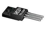
PINNING - SOT186A
PIN
BT258X series
QUICK REFERENCE DATA
SYMBOL
VDRM,
VRRM
IT(AV)
IT(RMS)
ITSM
PARAMETER
MAX. MAX. MAX. UNIT
BT258XRepetitive peak off-state
voltages
Average on-state current
RMS on-state current
Non-repetitive peak on-state
current
500R
500
600R
600
800R
800
V
5
8
75
5
8
75
5
8
75
A
A
A
PIN CONFIGURATION
mb
DESCRIPTION
1
cathode
2
anode
3
gate
SYMBOL
A
K
G
sym037
1 2 3
case isolated
TO-220F (SOT186A)
LIMITING VALUES
Limiting values in accordance with the Absolute Maximum System (IEC 134).
SYMBOL
PARAMETER
CONDITIONS
VDRM, VRRM Repetitive peak off-state
voltages
IT(AV)
IT(RMS)
ITSM
I2t
dIT/dt
IGM
VRGM
PGM
PG(AV)
Tstg
Tj
Average on-state current
RMS on-state current
Non-repetitive peak
on-state current
half sine wave; Ths ≤ 90 ˚C
all conduction angles
half sine wave; Tj = 25 ˚C prior to
surge
t = 10 ms
t = 8.3 ms
t = 10 ms
ITM = 10 A; IG = 50 mA;
dIG/dt = 50 mA/µs
I2t for fusing
Repetitive rate of rise of
on-state current after
triggering
Peak gate current
Peak reverse gate voltage
Peak gate power
Average gate power
over any 20 ms period
Storage temperature
Operating junction
temperature
MIN.
MAX.
UNIT
-
-500R -600R -800R
5001
6001
800
V
-
5
8
A
A
-
75
82
28
50
A
A
A2s
A/µs
-40
-
2
5
5
0.5
150
1252
A
V
W
W
˚C
˚C
1 Although not recommended, off-state voltages up to 800V may be applied without damage, but the thyristor may
switch to the on-state. The rate of rise of current should not exceed 15 A/µs.
2 Note: Operation above 110˚C may require the use of a gate to cathode resistor of 1kΩ or less.
September 2018
1
Rev 2.100
�WeEn Semiconductors
Product specification
Thyristors
logic level
BT258X series
ISOLATION LIMITING VALUE & CHARACTERISTIC
Ths = 25 ˚C unless otherwise specified
SYMBOL
PARAMETER
CONDITIONS
Visol
R.M.S. isolation voltage from all
three terminals to external
heatsink
f = 50-60 Hz; sinusoidal
waveform;
R.H. ≤ 65% ; clean and dustfree
Cisol
Capacitance from T2 to external f = 1 MHz
heatsink
MIN.
TYP.
MAX.
UNIT
-
-
2500
V
-
10
-
pF
MIN.
TYP.
MAX.
UNIT
-
55
5.0
6.9
-
K/W
K/W
K/W
MIN.
TYP.
MAX.
UNIT
0.1
-
50
0.4
0.3
1.3
0.4
0.2
0.1
200
10
6
1.6
1.5
0.5
µA
mA
mA
V
V
V
mA
MIN.
TYP.
MAX.
UNIT
50
100
-
V/µs
-
2
-
µs
-
100
-
µs
THERMAL RESISTANCES
SYMBOL
PARAMETER
CONDITIONS
Rth j-hs
Thermal resistance
junction to heatsink
Thermal resistance
junction to ambient
with heatsink compound
without heatsink compound
in free air
Rth j-a
STATIC CHARACTERISTICS
Tj = 25 ˚C unless otherwise stated
SYMBOL
PARAMETER
CONDITIONS
IGT
IL
IH
VT
VGT
Gate trigger current
Latching current
Holding current
On-state voltage
Gate trigger voltage
ID, IR
Off-state leakage current
VD = 12 V; IT = 0.1 A
VD = 12 V; IGT = 0.1 A
VD = 12 V; IGT = 0.1 A
IT = 16 A
VD = 12 V; IT = 0.1 A
VD = VDRM(max); IT = 0.1 A; Tj = 110 ˚C
VD = VDRM(max); VR = VRRM(max); Tj = 125 ˚C
DYNAMIC CHARACTERISTICS
Tj = 25 ˚C unless otherwise stated
SYMBOL
PARAMETER
CONDITIONS
dVD/dt
Critical rate of rise of
off-state voltage
Gate controlled turn-on
time
Circuit commutated
turn-off time
VDM = 67% VDRM(max); Tj = 125 ˚C;
exponential waveform; RGK = 100 Ω
ITM = 10 A; VD = VDRM(max); IG = 5 mA;
dIG/dt = 0.2 A/µs
VD = 67% VDRM(max); Tj = 125 ˚C;
ITM = 12 A; VR = 24 V; dITM/dt = 10 A/µs;
dVD/dt = 2 V/µs; RGK = 1 kΩ
tgt
tq
September 2018
2
Rev 2.100
�WeEn Semiconductors
Product specification
Thyristors
logic level
BT258X series
Ptot (W)
Ths(max) (˚C)
85
a = 1.57
90
8
conduction
angle
degrees
30
60
90
120
180
6
form
factor
(a)
1.9
4
2.8
2.2
1.9
1.57
2.2
2.8
4
4
2
0
0
4
2
IT(AV) (A)
I TSM
70
IT
95
60
100
50
time
T
Tj initial = 25 C max
105
40
110
30
115
20
120
10
125
0
6
Fig.1. Maximum on-state dissipation, Ptot, versus
average on-state current, IT(AV), where
a = form factor = IT(RMS)/ IT(AV).
1000
ITSM / A
80
1
10
100
Number of half cycles at 50Hz
1000
Fig.4. Maximum permissible non-repetitive peak
on-state current ITSM, versus number of cycles, for
sinusoidal currents, f = 50 Hz.
ITSM / A
24
IT(RMS) / A
20
16
dI T/dt limit
100
12
I TSM
IT
8
time
T
4
Tj initial = 25 C max
10
10us
100us
0
0.01
10ms
1ms
0.1
1
surge duration / s
T/s
Fig.2. Maximum permissible non-repetitive peak
on-state current ITSM, versus pulse width tp, for
sinusoidal currents, tp ≤ 10ms.
9
Fig.5. Maximum permissible repetitive rms on-state
current IT(RMS), versus surge duration, for sinusoidal
currents, f = 50 Hz; Ths ≤ 90˚C.
IT(RMS) / A
1.6
90 C
8
10
VGT(Tj)
VGT(25 C)
1.4
7
6
1.2
5
4
1
3
0.8
2
0.6
1
0
-50
0
50
Ths / C
100
0.4
-50
150
Fig.3. Maximum permissible rms current IT(RMS) ,
versus mounting base temperature Ths.
September 2018
0
50
Tj / C
100
150
Fig.6. Normalised gate trigger voltage
VGT(Tj)/ VGT(25˚C), versus junction temperature Tj.
3
Rev 2.100
�WeEn Semiconductors
Product specification
Thyristors
logic level
3
BT258X series
IGT(Tj)
IGT(25 C)
I /A
30 T
Tj = 125 °C
Tj = 25 °C
2.5
20
2
1.5
typ
10
1
max
Vo = 1 V
Rs = 0.04 Ω
0.5
0
-50
0
0
50
Tj / C
100
150
Fig.7. Normalised gate trigger current
IGT(Tj)/ IGT(25˚C), versus junction temperature Tj.
3
IL(Tj)
IL(25 C)
0
0.5
1
VT / V
1.5
2
Fig.10. Typical and maximum on-state characteristic.
10
BT150
Zth j-hs (K/W)
without heatsink compound
2.5
with heatsink compound
1
2
1.5
0.1
1
P
D
t
p
t
0.5
0
-50
0
50
Tj / C
100
0.01
10us
150
1ms
10ms
0.1s
1s
10s
tp / s
Fig.8. Normalised latching current IL(Tj)/ IL(25˚C),
versus junction temperature Tj.
3
0.1ms
Fig.11. Transient thermal impedance Zth j-hs, versus
pulse width tp.
IH(Tj)
IH(25 C)
1000
dVD/dt (V/us)
RGK = 100 ohms
2.5
100
2
1.5
10
1
0.5
0
-50
0
50
Tj / C
100
1
150
50
100
150
Tj / C
Fig.9. Normalised holding current IH(Tj)/ IH(25˚C),
versus junction temperature Tj.
September 2018
0
Fig.12. Typical, critical rate of rise of off-state voltage,
dVD/dt versus junction temperature Tj.
4
Rev 2.100
�WeEn Semiconductors
Product specification
Thyristors
logic level
BT258X series
MECHANICAL DATA
September 2018
5
Rev 2.100
�WeEn Semiconductors
Legal information
Data sheet status
Document
status [1][2]
Product
status [3]
Objective
[short] data
sheet
Development This document contains data from
the objective specification for product
development.
Preliminary
[short] data
sheet
Qualification
This document contains data from the
preliminary specification.
Product
[short] data
sheet
Production
This document contains the product
specification.
[1]
[2]
[3]
Definition
Please consult the most recently issued document before initiating or
completing a design.
The term 'short data sheet' is explained in section "Definitions".
The product status of device(s) described in this document may have
changed since this document was published and may differ in case of
multiple devices. The latest product status information is available on
the Internet at URL http://www.ween-semi.com.
Definitions
Draft — The document is a draft version only. The content is still under
internal review and subject to formal approval, which may result in
modifications or additions. WeEn Semiconductors does not give any
representations or warranties as to the accuracy or completeness of
information included herein and shall have no liability for the consequences
of use of such information.
Short data sheet — A short data sheet is an extract from a full data sheet
with the same product type number(s and title. A short data sheet is
intended for quick reference only and should not be relied upon to contain
detailed and full information. For detailed and full information see the
relevant full data sheet, which is available on request via the local WeEn
Semiconductors sales office. In case of any inconsistency or conflict with the
short data sheet, the full data sheet shall prevail.
Product specification — The information and data provided in a Product
data sheet shall define the specification of the product as agreed between
WeEn Semiconductors and its customer, unless WeEn Semiconductors and
customer have explicitly agreed otherwise in writing. In no event however,
shall an agreement be valid in which the WeEn Semiconductors product
is deemed to offer functions and qualities beyond those described in the
Product data sheet.
Disclaimers
Limited warranty and liability — Information in this document is believed to
be accurate and reliable. However, WeEn Semiconductors does not
give any representations or warranties, expressed or implied, as to the
accuracy or completeness of such information and shall have no liability for
the consequences of use of such information. WeEn Semiconductors takes
no responsibility for the content in this document if provided by an information
source outside of WeEn Semiconductors.
In no event shall WeEn Semiconductors be liable for any indirect, incidental,
punitive, special or consequential damages (including - without limitation lost profits, lost savings, business interruption, costs related to the removal
or replacement of any products or rework charges whether or not such
damages are based on tort (including negligence, warranty, breach of
contract or any other legal theory.
Notwithstanding any damages that customer might incur for any reason
whatsoever, WeEn Semiconductors’ aggregate and cumulative liability
towards customer for the products described herein shall be limited in
accordance with the Terms and conditions of commercial sale of WeEn
Semiconductors.
Right to make changes — WeEn Semiconductors reserves the right to
make changes to information published in this document, including without
limitation specifications and product descriptions, at any time and without
notice. This document supersedes and replaces all information supplied prior
to the publication hereof.
Suitability for use — WeEn Semiconductors products are not designed,
authorized or warranted to be suitable for use in life support, life-critical
or safety-critical systems or equipment, nor in applications where failure
or malfunction of an WeEn Semiconductors product can reasonably
be expected to result in personal injury, death or severe property or
environmental damage. WeEn Semiconductors and its suppliers accept no
liability for inclusion and/or use of WeEn Semiconductors products in such
equipment or applications and therefore such inclusion and/or use is at the
customer’s own risk.
Quick reference data — The Quick reference data is an extract of the
product data given in the Limiting values and Characteristics sections of this
document, and as such is not complete, exhaustive or legally binding.
Applications — Applications that are described herein for any of these
products are for illustrative purposes only. WeEn Semiconductors makes
no representation or warranty that such applications will be suitable for the
specified use without further testing or modification.
Customers are responsible for the design and operation of their applications
and products using WeEn Semiconductors products, and WeEn
Semiconductors accepts no liability for any assistance with applications or
customer product design. It is customer’s sole responsibility to determine
whether the WeEn Semiconductors product is suitable and fit for the
customer’s applications and products planned, as well as for the planned
application and use of customer’s third party customer(s). Customers should
provide appropriate design and operating safeguards to minimize the risks
associated with their applications and products.
WeEn Semiconductors does not accept any liability related to any default,
damage, costs or problem which is based on any weakness or default
in the customer’s applications or products, or the application or use by
customer’s third party customer(s). Customer is responsible for doing all
necessary testing for the customer’s applications and products using WeEn
Semiconductors products in order to avoid a default of the applications
and the products or of the application or use by customer’s third party
customer(s). WeEn does not accept any liability in this respect.
Limiting values — Stress above one or more limiting values (as defined in
the Absolute Maximum Ratings System of IEC 60134) will cause permanent
damage to the device. Limiting values are stress ratings only and (proper)
operation of the device at these or any other conditions above those
given in the Recommended operating conditions section (if present) or the
Characteristics sections of this document is not warranted. Constant or
repeated exposure to limiting values will permanently and irreversibly affect
the quality and reliability of the device.
No offer to sell or license — Nothing in this document may be interpreted
or construed as an offer to sell products that is open for acceptance or the
grant, conveyance or implication of any license under any copyrights, patents
or other industrial or intellectual property rights.
Export control — This document as well as the item(s) described herein
may be subject to export control regulations. Export might require a prior
authorization from competent authorities.
Non-automotive qualified products — Unless this data sheet expressly
states that this specific WeEn Semiconductors product is automotive
qualified, the product is not suitable for automotive use. It is neither qualified
nor tested in accordance with automotive testing or application requirements.
WeEn Semiconductors accepts no liability for inclusion and/or use of nonautomotive qualified products in automotive equipment or applications.
In the event that customer uses the product for design-in and use in
automotive applications to automotive specifications and standards,
customer (a) shall use the product without WeEn Semiconductors’ warranty
of the product for such automotive applications, use and specifications, and
(b) whenever customer uses the product for automotive applications beyond
WeEn Semiconductors’ specifications such use shall be solely at customer’s
own risk, and (c) customer fully indemnifies WeEn Semiconductors for
any liability, damages or failed product claims resulting from customer
design and use of the product for automotive applications beyond WeEn
Semiconductors’ standard warranty and WeEn Semiconductors’ product
specifications.
�WeEn Semiconductors
Translations — A non-English (translated version of a document is for
reference only. The English version shall prevail in case of any discrepancy
between the translated and English versions.
Trademarks
Notice: All referenced brands, product names, service names and
trademarks are the property of their respective owners.
�