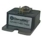
GA080TH65
Silicon Carbide Thyristor
Features
VFBM
=
6500 V
IT(AVM)
=
80 A
Qrr
=
4.2 µC
Package
6500 V Asymmetric SiC NPNP Thyristor
150 °C operating temperature
Robust compact fully soldered package
SOT-227 (ISOTOP) base plate form factor
Fast turn on characteristics
Lowest in class Qrr/IT(AVM)
Applications
Grid Tied Solar Inverters
Wind Power Inverters
HVDC Power Conversion
Utility Scale Power Conversion
Trigger Circuits/Ignition Circuits
Maximum Ratings
Parameter
Repetitive peak forward voltage
Repetitive peak reverse voltage
Maximum average on-state current
RMS on-state current
Non-repetitive peak on-state current
Power dissipation
Operating and storage temperature
Symbol
VFBM
VRBM
IT(AVM)
IT(RMS)
IT,max
Ptot
Tj, Tstg
Conditions
Values
6500
50
80
139
tbd
1563
-55 to 150
Tj = 25 °C
Tj = 25 °C
TC 125 °C
TC 125 °C
TC= 25 °C, tp = 2 us, D = 0.1
TC= 25 °C
Unit
V
V
A
A
A
W
°C
Electrical Characteristics
Parameter
Symbol
Maximum peak on state voltage
VKA(ON)
Anode-cathode threshold voltage
Anode-cathode slope resistance
VKA(TO)
RAK
Leakage current
Gate trigger current
Holding current
Rise time
Delay time
Reverse recovery charge
Recovered charge, 50% chord
Reverse recovery current
Circuit commutated turn-off time
IL
IGT
IH
tR
tD
Qrr
Qra
Irm
tq
Conditions
IK = -80 A, Tj = 25 °C
IK = -80 A, Tj = 150 °C
Tj = 25 °C (150 °C)
Tj = 25 °C (150 °C), IK = -80 A
VKA = -6500 V, V GA = 0 V, Tj = 25 °C
VKA = -6500 V, VGA = 0 V, Tj = 150 °C
Tj = 25 °C, tP = 10 µs
Tj = 25 °C
IG = -3 A, VKA = -2200 V
IK = -80 A, Tj = 25 °C
dI/dt = 430 A/us, IK = -70 A, VKA = 20 V
dV/dt(re-app) = -460 V/us, Tj = 25 °C
min.
Values
typ.
max.
-3.70
-3.45
-3.0(-2.7)
6.0(6.3)
15
50
-100
tbd
190
50
4.2
2.3
20
10.1
Unit
V
V
m
µA
mA
mA
ns
ns
µC
µC
A
µs
Thermal Characteristics
Thermal resistance, junction - case
RthJC
0.08
°C/W
1.5
1.3
30
Nm
Nm
g
Mechanical Properties
Mounting torque for base
Mounting torque for top
Weight
Mb
Mt
Wt
Heat sink surface must be optically flat
1. Considering worst case Zth conditions
http://www.genesicsemi.com/index.php/sic-products/thyristors
November 2010
Preliminary Datasheet
http://www.genesicsemi.com
Page 1 of 3
�GA080TH65
Figure 1: Typical On State Characteristics
Figure 2: Typical Forward Blocking Characteristics
Figure 3: Typical Current Derating Curves (D = tP/T, tP = 400 µs1)
Figure 4: Typical Current Rating versus Pulse Duration Curves
at TC = 120 OC
Figure 5: Typical Turn On Characteristics at 25 °C
November 2010
Figure 6: Typical Turn Off Characteristics at 25 °C
Preliminary Datasheet
http://www.genesicsemi.com
Page 2 of 3
�GA080TH65
Figure 7: Typical Reverse Recovery Characteristics at 25 °C
Figure 8: Typical Transient Thermal Impedance
Revision History
Date
2010/11/13
Revision
1
Comments
First generation release
Supersedes
Published by
GeneSiC Semiconductor, Inc.
43670 Trade Center Place Suite 155
Dulles, VA 20166
GeneSiC Semiconductor, Inc. reserves right to make changes to the product specifications and data in this document without notice.
GeneSiC disclaims all and any warranty and liability arising out of use or application of any product. No license, express or implied to any
intellectual property rights is granted by this document.
Unless otherwise expressly indicated, GeneSiC products are not designed, tested or authorized for use in life-saving, medical, aircraft
navigation, communication, air traffic control and weapons systems, nor in applications where their failure may result in death, personal injury
and/or property damage.
November 2010
Preliminary Datasheet
http://www.genesicsemi.com
Page 3 of 3
�
很抱歉,暂时无法提供与“GA080TH65-227SP”相匹配的价格&库存,您可以联系我们找货
免费人工找货