�WARRANTY
Parallax warrants its products against defects in materials and workmanship for a period of 90 days from receipt of product. If
you discover a defect, Parallax will, at its option, repair or replace the merchandise, or refund the purchase price. Before
returning the product to Parallax, call for a Return Merchandise Authorization (RMA) number. Write the RMA number on the
outside of the box used to return the merchandise to Parallax. Please enclose the following along with the returned merchandise:
your name, telephone number, shipping address, and a description of the problem. Parallax will return your product or its
replacement using the same shipping method used to ship the product to Parallax.
14-DAY MONEY BACK GUARANTEE
If, within 14 days of having received your product, you find that it does not suit your needs, you may return it for a full refund.
Parallax will refund the purchase price of the product, excluding shipping/handling costs. This guarantee is void if the product
has been altered or damaged. See the Warranty section above for instructions on returning a product to Parallax.
COPYRIGHTS AND TRADEMARKS
This documentation is Copyright 2003 by Parallax, Inc. By downloading or obtaining a printed copy of this documentation or
software you agree that it is to be used exclusively with Parallax products. Any other uses are not permitted and may represent a
violation of Parallax copyrights, legally punishable according to Federal copyright or intellectual property laws. Any duplication
of this documentation for commercial uses is expressly prohibited by Parallax, Inc. Check with Parallax for approval prior to
duplicating any of our documentation in part or whole for any use.
SX-Key is a registered trademark of Parallax, Inc. If you decide to use the name SX-Key on your web page or in printed material,
you must state that "SX-Key is a registered trademark of Parallax, Inc." Other brand and product names are trademarks or
registered trademarks of their respective holders
ISBN 1-928982-01-8
DISCLAIMER OF LIABILITY
Parallax, Inc. is not responsible for special, incidental, or consequential damages resulting from any breach of warranty, or under
any legal theory, including lost profits, downtime, goodwill, damage to or replacement of equipment or property, or any costs of
recovering, reprogramming, or reproducing any data stored in or used with Parallax products. Parallax is also not responsible for
any personal damage, including that to life and health, resulting from use of any of our products. You take full responsibility for
your SX-Key/Blitz and SX chip application, no matter how life-threatening it may be.
�WEB SITE AND DISCUSSION LISTS
The Parallax web site (www.parallax.com) has many downloads, products, customer applications and on-line ordering for the
components used in this text. We also maintain several e-mail discussion lists for people interested in using Parallax products.
These lists are accessible from www.parallax.com via the Support ? Discussion Groups menu. These are the lists that we operate:
§
§
§
§
§
§
§
SX Tech – Discussion of programming the SX microcontroller with Parallax assembly language tools and 3rd party
BASIC and C compilers. Approximately 600 members.
BASIC Stamps – With over 2,500 subscribers, this list is widely utilized by engineers, hobbyists and students who share
their BASIC Stamp projects and ask questions.
Stamps in Class – Created for educators and students, this list has 500 subscribers who discuss the use of the Stamps in
Class curriculum in their courses. The list provides an opportunity for both students and educators to ask questions and
get answers.
Parallax Educators – This focus group of 100 members consists exclusively of educators and those who contribute to the
development of Stamps in Class. Parallax created this group to obtain feedback on our curricula and to provide a forum
for educators to develop Teacher’s Guides.
Parallax Translators – Consisting of less than 10 people, the purpose of this list is to provide a conduit between Parallax
and those who translate our documentation to languages other than English. Parallax provides editable Word
documents to our translating partners and attempts to time the translations to coordinate with our publications.
Toddler Robot – A customer created this discussion list to discuss applications and programming of the Parallax
Toddler robot.
Javelin Stamp – Discussion of application and design using the Javelin Stamp, a Parallax module that is programmed
using a subset of Sun Microsystems’ Java® programming language. Approximately 250 members.
This manual is valid with the following software and firmware versions:
IDE:
SXKey.exe software version 2.0
Firmware:
SX-Key rev. F and SX-Blitz rev. A
The information herein will usually apply to newer versions but may not apply to older versions. New software can be obtained
free on our web site (www.parallax.com). If you have any questions about what you need to upgrade your product, please contact
Parallax.
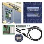
�Welcome
Thank you for purchasing the Parallax SX-Key/Blitz development system. We have done our best to
produce a full-featured, yet easy to use development system for the SX microcontrollers. The result is
the SX-Key and the SX-Blitz; very tiny, full-featured development tools with a Windows 95 and higher
versions interface. We hope you will find this system as enjoyable to use as we do.
This manual is written for the SX20/28 chips with a date code of AB9921AA or later, and SX48/52 chips
with a date code of AB0001A or later.
Older chips are not supported by this manual or the SX-Key development system.
�Table of Contents
Table of Contents
1
2
3
4
5
6
7
Introduction to the SX-Key/Blitz Hardware ................................................................................................................13
Installing the SX-Key/Blitz Software.............................................................................................................................15
Quick Start Introduction..................................................................................................................................................17
3.1
Connecting and Downloading to the SX Tech Board .......................................................................................17
The SX-Key/Blitz Interface .............................................................................................................................................19
4.1
Starting the SX-Key/Blitz Software ....................................................................................................................19
4.1.1
Command Line Switches ......................................................................................................................19
4.2
The SX Editor .........................................................................................................................................................20
4.3
The Menus..............................................................................................................................................................21
4.3.1
The File Menu ........................................................................................................................................21
4.3.2
The Edit Menu........................................................................................................................................22
4.3.3
The Run Menu........................................................................................................................................23
4.3.4
The Help Menu ......................................................................................................................................25
4.4
The Windows .........................................................................................................................................................25
4.4.1
Print Window.........................................................................................................................................25
4.4.2
Find Window .........................................................................................................................................26
4.4.3
Find/Replace Window .........................................................................................................................26
4.4.4
Goto Line Number Window ................................................................................................................27
4.4.5
Configure Window................................................................................................................................28
The SX-Key Debugger......................................................................................................................................................31
5.1
The Debugger Windows.......................................................................................................................................31
5.1.1
The Registers Window..........................................................................................................................31
5.1.2
The Debug Window ..............................................................................................................................34
5.1.3
The Watch Window...............................................................................................................................35
5.1.4
The Code/List File Window ................................................................................................................35
5.1.5
Modifying registers during debugging ..............................................................................................36
5.1.6
Breakpoints and the Current Instruction............................................................................................37
5.1.7
Setting the Program Counter ...............................................................................................................37
The Device Window.........................................................................................................................................................39
The SASM Assembler ......................................................................................................................................................43
7.1
The Structure of an SX Assembly Program........................................................................................................44
7.2
Comments ..............................................................................................................................................................45
7.3
Assembler Directives ............................................................................................................................................45
7.3.1
The EQU and = Directives....................................................................................................................47
7.3.2
The BREAK Directive............................................................................................................................47
7.3.3
The CASE and NOCASE Directives....................................................................................................47
7.3.4
The DEVICE Directive ..........................................................................................................................48
7.3.5
The DS Directive ....................................................................................................................................51
7.3.6
The DW Directive ..................................................................................................................................51
7.3.7
The END Directive ................................................................................................................................51
7.3.8
The ERROR Directive............................................................................................................................52
7.3.9
The FREQ Directive...............................................................................................................................52
7.3.10 The __FUSE and __FUSEX Directives.................................................................................................52
SX-Key/Blitz Development System Manual 2.0 • Parallax, Inc. • Page 5
�Table of Contents
8
7.3.11 The ID Directive.....................................................................................................................................53
7.3.12 The IF…ELSE…ENDIF Directive ........................................................................................................53
7.3.13 The IF{N}DEF…ELSE…ENDIF Directives .........................................................................................54
7.3.14 The INCLUDE Directive.......................................................................................................................55
7.3.15 The IRC_CAL Directive ........................................................................................................................56
7.3.16 The LIST Directive .................................................................................................................................56
7.3.17 The LPAGE Directive............................................................................................................................57
7.3.18 The ORG (Origin) Directive .................................................................................................................57
7.3.19 The RADIX Directive ............................................................................................................................58
7.3.20 The REPT Directive ...............................................................................................................................58
7.3.21 The RESET Directive .............................................................................................................................59
7.3.22 The SPAC Directive...............................................................................................................................59
7.3.23 The TITLE and STITLE Directives.......................................................................................................60
7.3.24 The WATCH Directive..........................................................................................................................60
7.4
Macros.....................................................................................................................................................................62
7.4.1
The MACRO Directive..........................................................................................................................62
7.4.2
The ENDM Directive.............................................................................................................................63
7.4.3
The EXITM Directive.............................................................................................................................63
7.4.4
The LOCAL Directive ...........................................................................................................................63
7.4.5
The EXPAND and NOEXPAND Directives.......................................................................................63
7.4.6
Formal Parameters.................................................................................................................................64
7.4.7
Macro Invocation...................................................................................................................................65
7.4.8
Actual Values of Parameters ................................................................................................................65
7.4.9
Token Pasting.........................................................................................................................................65
7.4.10 Quoting ...................................................................................................................................................65
7.4.11 Macro Examples.....................................................................................................................................66
7.4.11.1 Simple Macros with no Parameters.....................................................................................66
7.4.12 Macros with Formal Parameters by Count ........................................................................................67
7.4.13 Macros with Formal Parameters by Name.........................................................................................68
7.5
Symbols...................................................................................................................................................................68
7.6
Labels ......................................................................................................................................................................69
7.7
Expressions.............................................................................................................................................................70
7.8
Data Types..............................................................................................................................................................72
7.9
The __SASM Pre-Defined Constant ....................................................................................................................72
7.10 Files created by SASM ..........................................................................................................................................73
7.11 SASM Warning and Error Messages...................................................................................................................74
7.12 Reserved Words and Symbols .............................................................................................................................78
The Parallax Assembler ...................................................................................................................................................79
8.1
The Structure of an SX Assembly Program........................................................................................................79
8.2
Assembler Directives ............................................................................................................................................79
8.2.1
The Device Directive .............................................................................................................................79
8.3
Symbols...................................................................................................................................................................81
8.4
Labels ......................................................................................................................................................................81
8.5
Expressions.............................................................................................................................................................81
8.6
Error Messages.......................................................................................................................................................81
Page 6 • SX-Key/Blitz Development System Manual 2.0 • Parallax, Inc.
�Table of Contents
9
10
11
12
13
14
15
8.7
Data Types..............................................................................................................................................................83
8.8
Reserved Words and Symbols .............................................................................................................................84
Upgrading Existing Code for SASM ..............................................................................................................................85
SX Special Features and Coding Tips ............................................................................................................................87
10.1 Introduction ...........................................................................................................................................................87
10.2 Port Configuration and Usage .............................................................................................................................87
10.2.1 Port Direction .........................................................................................................................................88
10.2.2 Pull-Up Resistors ...................................................................................................................................89
10.2.3 Logic Level..............................................................................................................................................90
10.2.4 Schmitt-Trigger ......................................................................................................................................91
10.2.5 Edge Detection .......................................................................................................................................92
10.2.6 Wakeup (Interrupt) on Edge Detection ..............................................................................................93
10.2.7 Comparator ............................................................................................................................................95
10.3 The SX48/52 Multi-Function Timers ..................................................................................................................96
10.3.1 PWM Mode ............................................................................................................................................97
10.3.2 Software Timer Mode............................................................................................................................98
10.3.3 External Event Counter.........................................................................................................................98
10.3.4 Capture/Compare Mode......................................................................................................................98
10.4 All About Interrupts .............................................................................................................................................99
10.4.1 RTCC Rollover Interrupts...................................................................................................................100
10.5 Creating Tables ....................................................................................................................................................103
10.5.1 Data Tables ...........................................................................................................................................103
10.6 Dealing with Code Pages ...................................................................................................................................105
10.6.1 Branching Across Pages......................................................................................................................105
10.6.2 Calling Across Pages with Jump Tables ...........................................................................................106
Appendix A: SX Features ..............................................................................................................................................109
11.1 Introduction .........................................................................................................................................................109
11.2 CPU Features .......................................................................................................................................................109
11.3 Peripheral and I/O Features ..............................................................................................................................109
Appendix B: Instruction Set Overview........................................................................................................................111
12.1 Introduction .........................................................................................................................................................111
12.2 Instruction Set Summary ....................................................................................................................................111
12.3 Single Word Instructions....................................................................................................................................114
12.4 Multi-Word Instructions.....................................................................................................................................116
12.5 Instruction Set Quick Reference ........................................................................................................................118
Appendix C: SX Instruction Set ....................................................................................................................................121
13.1 Introduction .........................................................................................................................................................121
Appendix D: The SX Tech Board..................................................................................................................................145
14.1 SX Tech Board Features ......................................................................................................................................145
14.2 Connecting and Downloading...........................................................................................................................146
14.3 SX Tech Board Schematic ...................................................................................................................................147
Appendix E: SX Data Sheet ...........................................................................................................................................149
15.1 Pinout Information and Descriptions ...............................................................................................................149
15.2 Architecture..........................................................................................................................................................150
15.2.1 Instruction Pipeline .............................................................................................................................151
SX-Key/Blitz Development System Manual 2.0 • Parallax, Inc. • Page 7
�Table of Contents
15.3
15.4
15.2.2 Read-Modify-Write Considerations ..................................................................................................151
15.2.3 Register Map Structure .......................................................................................................................151
15.2.4 Special Function Registers..................................................................................................................153
15.2.5 IND – The Indirect Register ($00) ......................................................................................................153
15.2.6 Real Time Clock/Counter, WREG ($01)...........................................................................................153
15.2.7 PC – Program Counter ($02) ..............................................................................................................153
15.2.8 STATUS Register ($03)........................................................................................................................154
15.2.9 The FSR – File Select Register ($04) ...................................................................................................155
15.2.10 Direct Addressing................................................................................................................................156
15.2.11 Indirect Addressing.............................................................................................................................160
15.2.12 The Bank Instruction ...........................................................................................................................161
15.2.13 The Jump Instruction ..........................................................................................................................162
15.2.14 Jumping Across Pages.........................................................................................................................163
15.2.15 The Call Instruction.............................................................................................................................163
15.2.16 Calling Across Pages ...........................................................................................................................164
15.2.17 Returning from a subroutine..............................................................................................................164
15.2.18 The Stack...............................................................................................................................................165
15.2.19 The Push ...............................................................................................................................................165
15.2.20 The Pop .................................................................................................................................................166
15.2.21 Stack Overflow.....................................................................................................................................166
15.2.22 Stack Underflow ..................................................................................................................................166
15.2.23 Returns ..................................................................................................................................................166
Port Configuration Registers .............................................................................................................................167
15.3.1 Port A Registers ...................................................................................................................................167
15.3.1.1 TRIS_A – Data Direction Register......................................................................................167
15.3.1.2 LVL_A - TTL/CMOS Select Register ................................................................................167
15.3.1.3 PLP_A – Pull-Up Resistor Enable Register.......................................................................167
15.3.2 Port B Registers ....................................................................................................................................168
15.3.2.1 TRIS_B – Data Direction Register ......................................................................................168
15.3.2.2 LVL_B - TTL/CMOS Select Register.................................................................................168
15.3.2.3 PLP_B – Pull-Up Resistor Enable Register .......................................................................168
15.3.2.4 ST_B – Schmitt-Trigger Enable Register ...........................................................................169
15.3.2.5 WKEN_B – Wake Up Enable Register...............................................................................169
15.3.2.6 WKED_B – Wake Up Edge Select Register.......................................................................169
15.3.2.7 WKPND_B – MIWU Pending Register .............................................................................169
15.3.2.8 CMP_B – Comparator Enable Register .............................................................................170
15.3.3 Port C Registers....................................................................................................................................170
15.3.3.1 TRIS_C – Data Direction Register ......................................................................................170
15.3.3.2 LVL_C - TTL/CMOS Select Register.................................................................................170
15.3.3.3 PLP_C – Pull-Up Resistor Enable Register .......................................................................171
15.3.3.4 ST_C – Schmitt-Trigger Enable Register...........................................................................171
15.3.4 Port D and E Registers (SX48/52)......................................................................................................171
Control registers ..................................................................................................................................................171
15.4.1 Mode register (SX20/28).....................................................................................................................171
15.4.2 Mode register (SX48/52).....................................................................................................................173
Page 8 • SX-Key/Blitz Development System Manual 2.0 • Parallax, Inc.
�Table of Contents
15.4.3 Option ...................................................................................................................................................174
15.4.4 Fuse Registers.......................................................................................................................................174
15.5 Interrupts ..............................................................................................................................................................175
15.5.1 Description ...........................................................................................................................................175
15.5.2 The Specifics .........................................................................................................................................175
15.5.3 RTCC Interrupt ....................................................................................................................................175
15.5.4 RB0-RB7 Interrupt ...............................................................................................................................176
15.6 Peripherals............................................................................................................................................................176
15.6.1 Oscillator Driver ..................................................................................................................................176
15.6.1.1 LP, XT and HS Mode...........................................................................................................176
15.6.1.2 External RC Mode................................................................................................................178
15.6.1.3 Internal RC Mode.................................................................................................................179
16 Index ................................................................................................................................................................................181
SX-Key/Blitz Development System Manual 2.0 • Parallax, Inc. • Page 9
�Table of Contents
Figures
Figure 1 - Connecting the SX-Key/Blitz ................................................................................................................................ 13
Figure 2 - First Time Running Window................................................................................................................................. 16
Figure 3 - Configure Window................................................................................................................................................. 16
Figure 4 - SX Tech Board with SX chip inserted................................................................................................................... 17
Figure 5 - The SX-Key Icon...................................................................................................................................................... 19
Figure 6 - The SX Editor........................................................................................................................................................... 20
Figure 7 - The Find Window................................................................................................................................................... 26
Figure 8 - The Find/Replace Window................................................................................................................................... 26
Figure 9 - The Goto Line Number Window.......................................................................................................................... 27
Figure 10 - The Configure Window ....................................................................................................................................... 28
Figure 11 - The Debugger Windows ...................................................................................................................................... 33
Figure 12 - The Device Window ............................................................................................................................................. 39
Figure 13 - The Watch Window.............................................................................................................................................. 61
Figure 14 - TTL and CMOS Levels ......................................................................................................................................... 90
Figure 15 - Schmitt Trigger Characteristics........................................................................................................................... 91
Figure 16 - SX48/52 Multi-Function Timers ......................................................................................................................... 97
Figure 17 - The SX Tech Board.............................................................................................................................................. 145
Figure 18 - SX Tech Board Schematic................................................................................................................................... 147
Figure 19 - SX Pinouts............................................................................................................................................................ 149
Figure 20 - Instruction Pipeline ............................................................................................................................................ 151
Figure 21 - SX20/28 Register Map........................................................................................................................................ 152
Figure 22 - SX48/52 Register Map........................................................................................................................................ 152
Figure 23 - Rotate Right ......................................................................................................................................................... 155
Figure 24 - Rotate Left............................................................................................................................................................ 155
Figure 25 - Global Register Addressing SX20/28/48/52 (direct) .................................................................................... 156
Figure 26 - SX20/28 General Purpose Register Addressing (direct) ............................................................................... 157
Figure 27 - SX48/52 General-Purpose Register addressing (direct) ................................................................................ 158
Figure 28- SX20/28 Indirect register addressing................................................................................................................ 160
Figure 29 - SX48/52 Indirect register addressing............................................................................................................... 161
Figure 30 - The Jump Instruction.......................................................................................................................................... 162
Figure 31 - Jumping Across Pages........................................................................................................................................ 163
Figure 32 - The Call Instruction ............................................................................................................................................ 164
Figure 33 - Calling Across Pages .......................................................................................................................................... 164
Figure 34 - The Push............................................................................................................................................................... 165
Figure 35 - The Pop ................................................................................................................................................................ 166
Figure 36 - Prescaler Division Ratios ................................................................................................................................... 174
Figure 37 - SX with External Crystal.................................................................................................................................... 176
Figure 38 - SX with External Ceramic Resonator ............................................................................................................... 177
Figure 39 - SX with External System Clock ......................................................................................................................... 178
Figure 40 - External RC Mode............................................................................................................................................... 178
Page 10 • SX-Key/Blitz Development System Manual 2.0 • Parallax, Inc.
�Table of Contents
Tables
Table 1 - Editor Shortcut Keys ................................................................................................................................................ 21
Table 2 - Debugger Buttons and Shortcut Keys.................................................................................................................... 35
Table 3 – Register Editing Keys .............................................................................................................................................. 36
Table 4 - SX Clock Options...................................................................................................................................................... 40
Table 5 - SASM Directives ....................................................................................................................................................... 46
Table 6 - SX20/28 DEVICE Settings....................................................................................................................................... 49
Table 7 - SX48/52 DEVICE Settings....................................................................................................................................... 50
Table 8 – Comparison Operators........................................................................................................................................... 53
Table 9 - LIST Directive Options ............................................................................................................................................ 57
Table 10 - WATCH Display Formats ..................................................................................................................................... 60
Table 11 - Unary Operators ..................................................................................................................................................... 71
Table 12 - Binary Operators .................................................................................................................................................... 71
Table 13 - Data Types............................................................................................................................................................... 72
Table 14 - SASM Error and Warning Messages.................................................................................................................... 75
Table 15 - SASM Reserved Words.......................................................................................................................................... 78
Table 16 - Parallax Assembler DEVICE Options .................................................................................................................. 80
Table 17 - Parallax Assembler Error Messages..................................................................................................................... 81
Table 18 - Parallax Assembler Reserved Words ................................................................................................................... 84
Table 19 - Port Configuration Options................................................................................................................................... 87
Table 20 - MODE Register Settings ........................................................................................................................................ 88
Table 21 - Interrupt Timing ................................................................................................................................................... 102
Table 22 - SX Instruction Mnemonics .................................................................................................................................. 112
Table 23 - SX Single-Word Instructions ............................................................................................................................... 114
Table 24 - SX Multi-Word Instructions ................................................................................................................................ 116
Table 25 - SX Instruction Set Quick Reference.................................................................................................................... 118
Table 26 - Symbol and Value Operands .............................................................................................................................. 121
Table 27 - Flags and Registers............................................................................................................................................... 122
Table 28 - Binary Symbols ..................................................................................................................................................... 122
Table 29 - SX Pins ................................................................................................................................................................... 150
Table 30 - Special Function Registers................................................................................................................................... 153
Table 31 - Bank Addresses and FSR Values ........................................................................................................................ 159
Table 32 – SX20/28 Mode Register....................................................................................................................................... 172
Table 33 - SX48/52 Mode Register ....................................................................................................................................... 173
Table 34 – External Component Selection for Crystals (Vdd = 5V) ................................................................................. 177
Table 35 - Component Selection for Murata Ceramic Resonators (Vdd = 5.0 V) ........................................................... 177
SX-Key/Blitz Development System Manual 2.0 • Parallax, Inc. • Page 11
�Table of Contents
Page 12 • SX-Key/Blitz Development System Manual 2.0 • Parallax, Inc.
�1 Introduction the SX-Key/Blitz Hardware
1
Introduction to the SX-Key/Blitz Hardware
The SX-Key/Blitz hardware consists of the programmer unit, a four-pin programming interface and a
standard, female serial port connector (DB9). The serial port connector should be plugged into an
available standard, straight-through serial cable on an IBM-compatible PC. The four-pin connector on
the SX-Key/Blitz board should be connected to four pins (VSS, VDD, OSC2 and OSC1) of the SX chip.
Take care to connect it in the right orientation because this connector is not indexed.
Figure 1 - Connecting the SX-Key/Blitz
DB9 serial port
connector
28
MCLR
2
27
OSC1
n.c.
3
26
OSC2
VSS
4
25
RC7
n.c.
5
24
RC6
RA0
6
23
RC5
RA1
7
22
RC4
RA2
8
21
RC3
RA3
9
20
RC2
RB0
10
19
RC1
RB1
11
18
RC0
RB2
12
17
RB7
RB3
13
16
RB6
RB4
14
15
RB5
vF
Re
1
VDD
SX-28
RTCC
y
-Ke
X
S
+5
SX-Key or SX-Blitz
programmer device
OSC1
OSC2
VDD
VSS
+5
4-pin programming
interface
Vss
The SX-Key/Blitz is powered by the target circuit’s power supply and programming and debugging
takes place over the oscillator pins. The power supply to the SX-Key/Blitz must be +5 V DC. If an
external crystal, resonator or RC circuit is used, the SX-Key/Blitz can usually remain connected to the
SX chip for programming purposes, without affecting the operation of the circuit. When debugging, the
SX chip must not have an external clock source since the SX-Key’s internal programmable oscillator
must be used. The SX-Blitz can only program SX chips, it cannot debug them.
Each SX microcontroller contains the necessary debugger hooks required to perform SX in-circuit
debugging. No other supporting chips are necessary for the debugging process. During debugging, the
SX-Key provides the oscillator signal to drive the SX microcontroller until such time that a breakpoint is
hit or a single step or stop mode is initiated.
Figure 1 - Connecting the SX-Key/Blitz shows all the connections necessary to program, debug and run
the SX microcontroller. An external resonator or crystal should be connected to the OSC1 and OSC2
pins to run the SX if the SX-Blitz is used, or if the SX-Key’s internal clock oscillator is not used.
SX-Key/Blitz Development System Manual 2.0 • Parallax, Inc. • Page 13
�1 Introduction the SX-Key/Blitz Hardware
The SX-Blitz is designed to be a lower-cost device for programming the SX chips only (no debugging
features are available). The SX-Blitz and SX-Key use the same interface software for programming,
however, debugging features will not work with the SX-Blitz.
NOTE: Since the SX-Blitz and SX-Key function almost identically, they will be referred to as the SXKey/Blitz, except where there are distinct differences.
Page 14 • SX-Key/Blitz Development System Manual 2.0 • Parallax, Inc.
�2 Installing the SX-Key/Blitz Software
2
Installing the SX-Key/Blitz Software
Before following the steps in the next chapter, you should first install the SX-Key/Blitz interface on
your computer’s hard disk.
The SX-Key/Blitz Interface consists of the integrated editor, programmer, and debugger software. The
following system requirements are a minimum for using the SX-Key/Blitz Interface:
•
•
•
•
•
•
80486 (or higher) IBM or compatible PC;
Windows 95 or higher operating system;
64 Mb of RAM;
3 Mb of available hard drive space;
CD-ROM drive, or access to the Internet;
1 available serial port.
To install the SX-Key/Blitz Interface:
1.
Insert the Parallax CD-ROM in an available CD-ROM drive.
2.
Use the CD's automatic browser to navigate to the Software section.
3.
Expand the SX-Key & SX-Blitz folder.
4.
Select the 18/28/48/52-pin SX chips (SXKey.exe) item.
5.
Click on the Install button.
6.
When prompted for the type of installation, select “Typical” in order to have the software installed
in the “Programs\Parallax Inc\SX-Key v2.0” folder. Select “Custom” when you want to change the
default installation options, like the installation folder.
7.
After the setup has finished, you will find a shortcut on the desktop, and a new “Parallax Inc”
program group in the Start menu.
You may also download the software from the Parallax web site. There are two different file versions
available. One has a size of about 1.2 MB, and the other one of 4.6 MB. When you use the smaller one, it
is necessary to have an Internet connection active while installing the software. Select any folder where
the downloaded file shall be stored, and then run “Setup_SX-Key_Editor.exe” from this folder.
After you have successfully installed the SX-Key Editor and start it the first time, the dialog shown
below opens:
SX-Key/Blitz Development System Manual 2.0 • Parallax, Inc. • Page 15
�2 Installing the SX-Key/Blitz Software
Figure 2 - First Time Running Window
This is to remind you that you should review some basic configuration settings first. Click the OK button, and press Ctrl-U to open the Configuration dialog shown to the right.
The only setting that is important for now is the selection of the serial port to which you have connected
the SX-Key/Blitz.
Figure 3 - Configure Window
The configuration dialog allows you to select COM1, COM2, COM3, or COM4.
Click the radio button in the “Serial Port” section that matches your installation.
Make sure that the remaining options are set to the defaults as shown here, and then click “Okay” to
close the configuration dialog window.
You may keep the SX-Key Editor active because you will need it to perform the next steps below.
Page 16 • SX-Key/Blitz Development System Manual 2.0 • Parallax, Inc.
�3 Quick Start Instruction
3
Quick Start Introduction
This chapter is a quick start guide to connecting the SX-Key/Blitz and programming the SX
microcontroller. Without even knowing how the SX-Key/Blitz and the SX chip work, you should be
able to obtain satisfactory results from the steps that follow.
3.1
Connecting and Downloading to the SX Tech Board
In order to get familiar with how the SX-Key/Blitz Development System works, we’ll use the SX Tech
Board to program and run a 28-pin SX chip.
Keep in mind that the SX Tech Board is not a programmer; rather the SX-Key/Blitz is the
programmer/debugger device while the SX Tech board is a type of prototyping board. Follow these
steps to connect and download a program:
Figure 4 - SX Tech Board with SX chip inserted
Power
Jack
Power
Indicator
Resonator
Socket
Breadboard
Prototyping
Area
4-pin Programming
Header
SX microcontroller (28-pin DIP) properly
inserted into LIF socket.
Reset
Button
1) Plug an SX28AC/DP into the 28-pin LIF socket on the SX Tech board as shown in Figure 4 - SX Tech
Board with SX chip inserted. Make sure it is oriented so that the half-moon notch in the chip faces
away from the “Reset” button.
SX-Key/Blitz Development System Manual 2.0 • Parallax, Inc. • Page 17
�3 Quick Start Instruction
2) Connect the SX-Key/Blitz to a serial cable, and the serial cable to the serial (COM) port on the PC
that you have selected in the “Configure” dialog of the SX-Key/Blitz software.
3) Connect the SX-Key/Blitz to the 4-pin programming header with the VSS, VDD, OSC2 and OSC1
indicators lining up with the same indicators on the board Note that the programming header is not
indexed. Therefore, double-check the correct orientation of the SX-Key/Blitz.
4) Insert one end of a 470 ohm resister into the RC7 socket (next to the upper left side of the
breadboard). Insert the other end of the resister into any hole in the breadboard.
5) Insert the shorter leg of an LED into the breadboard hole that is closest (horizontally) to the resister
leg. Insert the other leg of the LED into one of the VDD sockets (next to the top side of the breadboard).
6) Plug the power supply into the SX Tech board and into an available wall outlet. (The power
indicator should light up).
7) If it is not still active, start the SX-Key Editor now.
8) In the SX-Key Editor window, pull down the File menu and select “Open” (or press Ctrl-O). In the
browser window that appears, select and open the led28.src file. (The led28.src source code should
appear in the SX-Key code window).
9) Pull down the Run menu and select Run (or press Ctrl-R). (The SX-Key software should assemble
the code and begin the programming process).
Congratulations! You have just programmed the SX microcontroller with the SX-Key/Blitz
Development System. The program in the SX microcontroller should start running. The LED should
flash on and off (if wired correctly).
In case you get an error message after you have selected the “Run” option, make sure that you did not
modify the source code text in the editor window. If you did, simply re-load the original text by
opening it again, and then repeat the steps described above.
Should an error message like “SX-Key not found on COMx” appear, check that you have selected the
right serial port for communication with the SX-Key/Blitz, and that the serial cable is correctly
connected to the PC, and to the SX-Key/Blitz on the other end. Also make sure that the SX-Key/Blitz is
correctly placed on the 4-pin programming header, and that the SX Tech board is powered, i.e. the
power indicator LED is active.
Page 18 • SX-Key/Blitz Development System Manual 2.0 • Parallax, Inc.
�4 The SX-Key/Blitz Interface
4
The SX-Key/Blitz Interface
The SX-Key/Blitz interface is an integrated editor, programmer, and debugger. All the functions of the
SX-Key and the SX-Blitz are available through this single software interface.
Throughout the rest of this manual, the SX-Key/Blitz interface will be referred to as the SX editor, or
more simply, the editor.
4.1
Starting the SX-Key/Blitz Software
Figure 5 - The SX-Key Icon
During installation, a shortcut was automatically placed on the Windows desktop. Double-click on the
SX-Key icon to launch the SX-Key/Blitz interface. In case, the Icon has been deleted from the desktop,
you can also start the software via the Windows Start button. Navigate to the Parallax Inc. program
group and select “SX-Key v2.0” there.
4.1.1
Command Line Switches
It is also possible to start the SX-Keys software together with parameters from a command line, e.g.
using the Windows “Run…” option, or from the DOS command line. The Syntax is:
SxKey / {/…}
When you specify a file name with a “.src” extension, the editor window will open, displaying the
contents of the source code file. When you specify an “.sxh” extension instead, the hex file will be
opened into the device window.
The /r switch is used to open a file in read-only mode, i.e. it can be displayed but not modified in the
editor or in the device window.
For example
SxKey /r test.src
opens the source file named “test”, and displays it in the editor window and
SxKey /r test.sxh
opens the hex file named “test”, and displays the device window. In both examples, the files are opened
read-only, i.e. they cannot be modified.
In addition to the /r switch, the switches /1, /2, /3 and /4 are also defined. They are used to select the
COM port where the SX-Key/Blitz is attached. This will override the setting that has been recently
SX-Key/Blitz Development System Manual 2.0 • Parallax, Inc. • Page 19
�4 The SX-Key/Blitz Interface
made in the Configure window. It is recommended not to use these switches; they have been
implemented for compatibility reasons only.
4.2
The SX Editor
Figure 6 - The SX Editor
The SX editor (see Figure 6 – The SX Editor, above) consists of a window containing a menu at the top,
several shortcut buttons in a tool bar, a list of files that are currently open to the left, and a large text
area to the right. In the status bar at the bottom, there is the row/column indicator, telling you at which
row and column the cursor is currently located. The editor window is where your SX source code will
be entered and edited. Standard Windows editing shortcut keys listed in Table 1 – Editor Shortcut
Keys, below, may be used in addition to the commands in the Edit menu and the tool bar buttons to
manipulate the source code.
Page 20 • SX-Key/Blitz Development System Manual 2.0 • Parallax, Inc.
�4 The SX-Key/Blitz Interface
Table 1 - Editor Shortcut Keys
Function
Name
Shortcut Function Description
Keys
Copy
Ctrl-C
Cut
Ctrl-X
Cuts selected text to the clipboard.
Paste
Ctrl-V
Pastes clipboard contents.
Page Up
PgUp
Moves editor window one page up.
Page Down
PgDn
Move editor window one page down.
Begin of Line
Home
End of Line
End
Begin of Text Ctrl-Home
4.3
Copies selected text to the clipboard.
End of Text
Ctrl-End
Tab
Tab
Move the cursor to column 1 in the current line
Move the cursor behind the last character in the line.
Moves the cursor to row 1, column 1 in the editor window.
Moves the cursor behind the last character of the text in the editor.
Moves cursor to the next tab position. The tab position can be set in the configuration dialog.
The Menus
The SX editor menu bar contains four menus: File, Edit, Run and Help. These menus and their associated
menu items are each described below. The most important functions can be also selected with one of the
shortcut buttons in the tool bar that are also shown below. You will find details to some of the functions
that can be selected via the menus later in this manual.
4.3.1
New
The File Menu
Creates a new, empty edit window. Use this item to start a new source code
editing session. You may also click the shortcut button to create a new file. When
you start the editor software, a blank session will be opened automatically, called
“Blank 1”.
When you select “New” while another editing session is already open, it will be
moved to the “background” but it will still remain open. The open files list to the
left displays the names of all open sessions.
Open…
Opens a browse window to locate and load source code files. As an alternative,
click the shortcut button, or type Ctrl-O to open an existing file.
Again, if there is another session already open, it will be moved to the
background.
The names of all currently open files are listed in the open files list to the left of
the editor window. To switch between the sessions, left-click on the name of the
file you want to see in the foreground.
SX-Key/Blitz Development System Manual 2.0 • Parallax, Inc. • Page 21
�4 The SX-Key/Blitz Interface
Closes the source code file currently displayed in the editor window. You may
also right-click on the file name in the open files list, and then left-click on the
prompt that is displayed to close a file.
Close
When the file to be closed has been modified since the last save, a dialog box will
open allowing you to select whether or not to save the file or abort the close
operation; i.e. keep the file open in the editor.
Save
Saves the source code file currently displayed in the editor window. The shortcut
button or Ctrl-S can also be used to save the file.
Save As…
Opens a Save As dialog box to save the source code currently displayed in the
editor window with a designated name.
Reopen
Displays a list of the files that were most recently edited. You may then click on
one of the list items to open any of these files directly.
Print…
Opens a print dialog box to print the source code currently displayed in the
editor window.
Exit
Terminates the SX-Key/Blitz editor.
4.3.2
The Edit Menu
Undo
This menu selection remains inactive until you make a change to the text in the
editor window. You can then revert the recent changes you have made to the
text. Ctrl-Z also activates the Undo function.
Redo
This is the opposite of the Undo function. It allows you to restore any changes
that were reverted by previous Undo actions. This selection remains inactive
until you have used the Undo function at least once. Ctrl-Y also does a redo.
After you have re-done an operation, you may undo it again.
Cut
Cuts the selected text from the editor window and stores it in the Windows
clipboard. Ctrl-X is the equivalent keyboard entry.
To select text, use one of the standard Windows methods, like moving the mouse
pointer across the text to be marked with the left mouse button pressed, or move
the cursor with the cursor keys while the Shift key is held down.
In order to select complete lines in the text, move the mouse cursor to the left
margin of the text area until it turns into an arrow, and then click the left mouse
button. To mark two or more lines, mark the first line, and then drag the mouse
up or down.
Page 22 • SX-Key/Blitz Development System Manual 2.0 • Parallax, Inc.
�4 The SX-Key/Blitz Interface
Copy
Copies the selected text from the editor window and stores it in the Windows
clipboard. Ctrl-C is the equivalent keyboard entry.
Paste
Pastes the text from the Windows clipboard into the editor window starting at
the current cursor location. Alternatively, type Ctrl-V to paste text.
Find
Opens
the Find dialog box. Ctrl-F is the shortcut key for this function. Enter the
text (or part of it) you are looking for. If necessary, you may select the options to
search for whole words only, or to match upper- and lower-case characters. You
can also specify the search direction, i.e. if the search shall be performed beginning at the current cursor position towards the beginning or end of the text.
Find Next
Finds the next occurrence of the specified text from the most recent Find
operation. F3 also performs this function.
Find/Replace…
Opens the standard Windows replace dialog box. Ctrl-H is the shortcut key for
this function. Again, you have the options to search for whole words only, or to
match upper- and lower-case characters.
Go to Line Number
Opens a dialog box where you can enter a line number. Ctrl-G is the shortcut key
for this function. Click “Ok” to close the dialog, and to position the cursor to
column 1 in the specified line.
Clear Errors
When errors are encountered while assembling a source code file with the “new”
default SASM assembler, the lines with errors are highlighted, and the errors
found are displayed in the status area. Use this menu selection to clear all error
information.
4.3.3
The Run Menu
Assemble
Assembles the code. You may also press Ctrl-A, or click the shortcut button to
start the assembly. When the code in the editor window could be assembled
without errors, the message “Assembly Successful” will show up in the status
bar.
When you use the default “new” SASM assembler and if there are any errors
encountered in the code, a message box will open, telling you that errors were
found. Click “Ok” to close the box. At the bottom of the editor window, you will
notice a new area that contains a list of all errors found during assembly. The first
error message line is highlighted, and the offending line in the source code is also
automatically highlighted.
When there are two or more error lines, double-click on a line in order to jump to
the offending line in the source code.
SX-Key/Blitz Development System Manual 2.0 • Parallax, Inc. • Page 23
�4 The SX-Key/Blitz Interface
Make the necessary corrections to the source code, and assemble the code again,
until no more errors are reported.
The assembler may also generate warning messages that are shown in the same
area, together with any errors. With warnings, the code will be assembled, but it
is a good idea to make the necessary corrections to the source code in order to
avoid warnings.
NOTE: Before assembly, the current file will be saved automatically. If you have
entered code into a new blank editor window, use the Save function to save the
window contents under a specific name before starting the assembler.
Program
Assembles the source code and programs the SX microcontroller (when the
assembly was successful). Ctrl-P also starts programming.
Run
Assembles the source code, programs the SX and generates a clock signal. Ctrl-R
also runs a program.
Debug
Assembles the source code, programs the SX, generates a clock signal and
initiates the debug mode. (Not used on the SX-Blitz). Ctrl-D also starts the
debugging mode.
Debug (reenter)
Assembles the source code, assumes that the SX device is already programmed
with the recent code to be debugged (i.e. does not program the SX again),
generates a clock signal and enters the debug mode. (Not used on the SX-Blitz).
Ctrl-Alt-D also re-enters the debugger.
This option is handy when you have previously terminated a debug session that
you want to continue later without having made changes to the source code in
the meantime.
As long as you add, remove or change WATCH or BREAK directives in the
source code, you may still use this function to reenter the debugging session
without downloading the program to the SX.
Any other changes to the source code require a new download, i.e. you must use the
Debug option instead, to start the debugger.
Page 24 • SX-Key/Blitz Development System Manual 2.0 • Parallax, Inc.
�4 The SX-Key/Blitz Interface
View List
Assembles the source code, and then opens another window that shows the
contents of the list file generated by the assembler. Ctrl-L also displays the list
file. The list file will be described in detail later in this manual (see Chapter 7.10 –
Files Created by SASM).
Clock…
Opens the clock control dialog box to allow the modification of the clock activity
and frequency. (Not used on the SX-Blitz). Ctrl-K also opens the clock dialog.
With this function, the SX device’s clock is supplied by the SX-Key, and you may
test the functionality of an application at various clock rates.
Device…
Opens the device dialog box to allow modification of the SX microcontroller parameters. Ctrl-I also opens the device dialog box.
Configure…
Opens
4.3.4
the configuration dialog box to allow modification of the SX-Key/Blitz
programming interface. See Chapter 4.4.5 – Configure Window for configuration
details. Ctrl-U also performs this operation.
The Help Menu
Contents
Displays information on how to use the WATCH and BREAK directives.
About
Displays the SX-Key/Blitz Development System information box.
4.4
The Windows
Many menu items open up a separate window for further configuration or monitoring. These windows
are described below.
4.4.1
Print Window
The print window is accessed via the Print… item on the File menu. It is the standard Windows Print
dialog box that you know from other applications. It allows you to select which printer shall be used,
and depending on the printer type, various options can be selected.
SX-Key/Blitz Development System Manual 2.0 • Parallax, Inc. • Page 25
�4 The SX-Key/Blitz Interface
4.4.2
Find Window
Figure 7 - The Find Window
The Find window is accessed via the Find item on the Edit menu. Enter the text to be searched for in the
“Find what” field. By default, the search direction is from the current cursor position to the bottom of
the text. You may change this direction by clicking the “Up” radio button in the “Direction” group.
You may also specify if the search shall match whole words only and if upper/lower case characters
shall be distinguished.
Click the “Find Next” button to start the search. When the pattern you have entered was found in the
text, it will be highlighted.
Clicking “Find Next” again continues the search, and the next match will be selected in the text (if any).
The Find window remains open, until you click the “Cancel” button.
After you have closed the Find window, you may still continue searching for the pattern most recently
entered by selecting “Find Next” in the Edit menu, or simply hit the F3 key to continue the search.
4.4.3
Find/Replace Window
Figure 8 - The Find/Replace Window
Page 26 • SX-Key/Blitz Development System Manual 2.0 • Parallax, Inc.
�4 The SX-Key/Blitz Interface
This window is similar to the Find window. Again, you can enter the text pattern to be searched for. In
addition, you also can enter the replacement text.
Also, you may select if only whole words should be found and if the search shall be case-sensitive, or
not.
Click the “Find Next” button to start the first search. When the pattern was found, it will be highlighted
in the text.
Click the “Replace” button to replace the highlighted text with the replacement you have entered, or
click “Find Next” to not alter the text, and to continue the search for the next matching pattern in the
text.
When wish to replace all occurrences of the search pattern, click the “Replace All” button. You should
use the replace all feature with extra caution because it replaces the search pattern in the whole text
without further confirmation. You might consider activating the “whole words only” option to avoid
unwanted replacements. Also note that “Replace All” always performs the search from the top of the
text down to the bottom, where the find next always continues towards the bottom of the text.
4.4.4
Goto Line Number Window
Figure 9 - The Goto Line Number Window
This window is accessed via the Goto Line Number item on the Edit menu. Enter the line number where
the cursor shall be positioned and click Ok. If necessary, the text in the editor window will be scrolled
so that the line you have addressed will be visible and the cursor is placed in column 1 of this line.
SX-Key/Blitz Development System Manual 2.0 • Parallax, Inc. • Page 27
�4 The SX-Key/Blitz Interface
4.4.5
Configure Window
Figure 10 - The Configure Window
This window is accessed via the Configure item on the Run menu and allows you to setup various
properties of the software.
We have already addressed the Serial Port section at the top of the window. Click one of the radio
buttons to select the COM port where your SX-Key/Blitz is connected.
When the option Create backup (.bak) files is selected, the editor will save a copy of the previous version
whenever a modified source code file is saved.
The group Assembler Options allows you to configure the SASM assembler.
When Use SASM is selected, the editor will call SASM to translate the source code in the editor window
into SX machine code. SASM is an enhanced version of Ubicom’s SASM assembler that has been
adapted to the SX-Key Version 2 software. When you un-check this option, the original Parallax
assembler will be invoked instead. Because there are some differences in language syntax between the
two assemblers, it might be necessary to use the Parallax Assembler with older, legacy, source code (see
Chapter 7 – The SASM Assembler and Chapter 8 – The Parallax Assembler for the differences
between the assemblers).
Page 28 • SX-Key/Blitz Development System Manual 2.0 • Parallax, Inc.
�4 The SX-Key/Blitz Interface
Nevertheless, we strongly recommend that you use the SASM assembler for all new, or recently revised,
source code. There are only a few modifications necessary to make legacy source code compatible with
SASM (see Chapter 9 – Upgrading Existing Code for SASM).
When you choose to use the Parallax Assembler, by un-checking the "Use SASM" box, you will notice
that a new group is shown at the top of the Options window, called IRC Calibration. Since the Parallax
Assembler does not accept directives in the source code to set the value for IRC calibration, it is
necessary to do this “outside” of the source code (see Chapter 15.6.1.3 – Internal RC Mode for details
on IRC calibration).
When the option SASM files to “SASM Output dir” is selected, the files generated by SASM will be
stored in the folder named “SASM Output” that is located in the folder where the SX-Key software has
been installed. When the option is de-selected, the files will be stored in the folder where the source
code files are located. See Chapter 7.10 – Files Generated by SASM for an explanation of the output
files generated by SASM.
The option Local Labels Must Start In Col. 1 controls how SASM searches the source code for local labels
(see Chapter 7.6 - Labels for more details on local labels). When the option is selected, local labels must
start in the first column of a source code line. Otherwise, local labels may be indented.
When the Use New Editor option is un-checked, the text editor will change its style into the editor format
that was part of earlier versions of the SX-Key software. As this “old” editor has much less features, it is
recommended to always use the “new” editor. You will notice that the remaining selections in the
Configure window will become invisible when you select the “old” editor.
The Enhanced Editor Options group contains various selections that allow you to configure the “new”
editor.
Use the upper left and right arrow buttons to change the Font size of the text displayed in the editor
window between 6 and 32 points.
The left and right arrow buttons below let you define the Tab size, i.e. by how many columns text shall
be indented on TAB characters in the text (2, 4, 6, or 8 columns).
When Colored Code Keywords is checked, the editor will perform “syntax highlighting”, i.e. keywords in
the source code text are displayed in color. Click on the colored button to the right of this option to open
the Color dialog box. Here you can select the color that shall be used to highlight the keywords.
The Boldface Code Keywords gives you the option to let the editor display keywords in boldface.
Boldfacing and color highlighting may also be combined.
When the Colored Comments option is checked, any comments in the source code text, i.e. text that starts
with a semicolon, will be displayed in the color indicated to the right of this option. The color can be
changed by clicking on the colored button.
SX-Key/Blitz Development System Manual 2.0 • Parallax, Inc. • Page 29
�4 The SX-Key/Blitz Interface
The next option, Error BG Color, allows you to select the background color that shall be used to highlight
any lines with errors after assembly. Again, click on the colored button to open the Color dialog box.
When the Jump To Assembly Error Line option is checked, the cursor will be positioned on the first line in
the source code text after assembly, when errors were encountered. In addition, this line will be
highlighted with the background color you have selected for the previous option.
After you have selected the required options, click “Okay” to accept them and to close the Configure
window. Click “Cancel” instead, when you want to keep the options unchanged.
Page 30 • SX-Key/Blitz Development System Manual 2.0 • Parallax, Inc.
�5 The SX-Key Debugger
5
The SX-Key Debugger
The following is required to use the debug features:
•
SX-Key Rev. E (or greater) – The SX-Blitz cannot be used for debugging.
•
SX chip date code 9825 or later.
•
No external clock source connected to the SX chip. This includes oscillator packs, crystals,
resonators and RC circuits.
•
The SX-Key connected to the 4-pin programming header of the SX system to be debugged.
•
The SX system must be powered.
Source code to be debugged must include the RESET directive (see Chapter 7.3.21), must have
WATCHDOG set to off, and must have 2 free words in the first page of code and 136 free words near
the end of the last page of code (from 177 to 1FE, 377 to 3FE, 577 to 5FE, 777 to 7FE, 977 to 9FE, B77 to
BFE, D77 to DFE, F77 to FFE), depending on the number of E2Flash pages. If an oscillator frequency of
other than 50 MHz (the default) is desired, the source code should contain a FREQ directive (see
Chapter 7.3.9) stating the frequency. When the FREQ directive is missing, the assembler will generate a
warning message, indicating that 50 MHz is used by default.
NOTE: On some machines, it is necessary to close background software (graphics, screen savers, etc.), for proper
operation of the DEBUG windows.
In order to invoke the debugger, select “Debug” from the “Run” menu, press Ctrl-D, or click the debug
shortcut button in the tool bar.
The source code that is currently displayed in the editor window will be assembled, and if no errors
were found, the program is automatically transferred into the program memory of the SX device.
If the transfer was successful, and if an IRC Calibration setting of 4 MHz was chosen, a small window
with IRC information is displayed. You may ignore this information for now, and click “Okay” to close
the window (see Chapter 15.6.1.3 – Internal RC Mode for details on IRC calibration).
Next, the debugger will start, and the windows will be displayed as shown in Figure 11 – The
Debugger Windows.
5.1
5.1.1
The Debugger Windows
The Registers Window
This window contains all the data and describes the current state of the SX chip. The leftmost column
within the Registers window displays the hexadecimal contents of global registers $00 through $0F.
SX-Key/Blitz Development System Manual 2.0 • Parallax, Inc. • Page 31
�5 The SX-Key Debugger
Registers $10 through $1F of all other banks are shown in the columns on the far right of the window.
The bank offsets are labeled at the top of each column and the current bank is highlighted in white.
These columns will expand or contract to fit the number of RAM banks available in the SX. In this
example, eight banks are shown.
The blue outline, shown here on the IND register, indicates the location that the FSR (file select register)
is currently pointing at.
The second column, just to the right of the first sixteen registers, displays a binary representation of
some of the registers, namely IND, Status, RA, RB, RC and 08 through 0F.
At the top center of the Registers window are the contents of the M register (hexadecimal) and the W
register (both hexadecimal and binary) and the Interrupt and Skip flags. The Interrupt and Skip flags
turn blue when set and white when cleared. The interrupt flag is set when an interrupt has occurred
and cleared after the interrupt has been serviced. The Skip flag is set when the compare condition
evaluates to true, i.e. when the skip will be performed. It is cleared when the condition evaluates to
false, or after the skip has been performed.
Page 32 • SX-Key/Blitz Development System Manual 2.0 • Parallax, Inc.
�5 The SX-Key Debugger
Figure 11 - The Debugger Windows
The assembly code box under the M and W register display in the center of the Registers window lists
several contiguous instructions at once. The first three digits on each line is the hexadecimal address in
program memory, followed by the opcode and finally the assembly mnemonic and operand(s). This
window normally shows the active section of code, around which the program counter (PC) points,
however, the scroll bar allows movement of the window’s field of view to any section of code.
SX-Key/Blitz Development System Manual 2.0 • Parallax, Inc. • Page 33
�5 The SX-Key Debugger
5.1.2
The Debug Window
The Debug window contains buttons for debugging functions. Each button has an associated shortcut
key, as described in Table 2 – Debugger Buttons and Shortcut Keys, below.
•
The Step button (or Alt-S) will execute one machine instruction and update all registers.
•
The Walk button (or Alt-W) will execute one machine instruction after another in “slow motion”,
updating the display automatically and continuing until the Stop button is pressed, or a breakpoint
is encountered. The delay time between instruction executions can be selected from the Update Speed
drop-down list; with the range being from 1 (about one second) to Max (as fast as the computer can
process it).
•
The Run button (or Alt-R) will initiate a full-speed execution of the program, and will continue until
a breakpoint is hit or the Stop or Reset buttons are pressed. The displayed registers will not update
until the Poll button is pressed or execution is stopped.
•
The Poll button (or Alt-L) operates in one of two modes. If a breakpoint exists, the Poll button runs
the code at full speed halting execution at the break just long enough to update the display and then
continues running. If a breakpoint is not set, the Poll button can be pressed only during run mode to
get an instant update of the register displays.
•
The Stop button (or Alt-P) halts execution of a walk, run or poll operation and updates the display.
•
The Reset button (or Alt-T) returns the SX chip to its initial state and sets the program counter (PC)
to the location containing the reset vector.
•
The Registers, Code and Watch buttons (or Alt-E, Alt-D, Alt-C) bring the associated windows into
view if they were hidden. (The Debug window always stays on top).
•
The Reset Pos. button brings all windows into view, places them at their default positions, and
resizes them to the defaults.
•
The Quit button (or Alt-Q) closes the Debug windows and exits debug mode.
Page 34 • SX-Key/Blitz Development System Manual 2.0 • Parallax, Inc.
�5 The SX-Key Debugger
Table 2 - Debugger Buttons and Shortcut Keys
Button
Shortcut
Step
Alt-S
Function
Executes one machine instruction.
Walk
Alt-W
Executes multiple machine instructions in “slow motion”.
Run
Alt-R
Poll
Alt-L
Stop
Alt-P
Executes instructions in full speed.
Updates display then continues execution. Can be used synchronously or
asynchronously.
Halts execution of a walk or run operation.
Reset
Alt-T
Resets the SX chip.
Registers
Alt-E
Brings Registers window into view.
Code
Alt-D
Brings Code window into view.
Watch
Alt-C
Brings Watch window into view.
Reset Pos.
none
Resets all debugger windows to their defaults.
Quit
Alt-Q
Closes the Debug Windows and exits debug mode.
The Debug windows are highly active and interactive displays. Every time the display is updated (after
a step, walk, poll or stop operation), each register that was modified since the previous update is highlighted in red. This provides a clear indication of what the last instruction accomplished. Similarly, each
bit that was changed is marked in red within all registers shown in binary. Additionally, the assembly
code box and Code window highlights the instruction pointed to by the program counter (PC) in blue,
and a breakpoint in red.
5.1.3
The Watch Window
The Watch window displays the contents of selected registers in a user-defined format. The values in
the Watch window can be modified using the same methods described in Section 5.1.5 – Modifying
registers during debugging, below. In addition, the numerical values in the Watch window can be
modified in any format (binary, hexadecimal or decimal) regardless of the displayed format. Simply
precede the input value with a %, $, or nothing, respectively. String values can only be modified by
entering new strings. See the Watch directive section in Chapter 7.3.23 – The Watch Directive for
information of defining watches.
5.1.4
The Code/List File Window
This window displays the contents of the list file generated by the assembler (see Chapter 7.10 – Files
Created by SASM for more information about the list file). While a program is executed in single steps,
or in walk mode, the instruction that is currently executed is highlighted with a blue background.
If a breakpoint is defined, this line is highlighted with a red background.
The Code/List File window has a toolbar with several shortcut buttons. These buttons have the
following meanings:
SX-Key/Blitz Development System Manual 2.0 • Parallax, Inc. • Page 35
�5 The SX-Key Debugger
Jump to Code: Scrolls the window to display the first line that assembles into CPU instructions.
Jump to Reset Line: Scrolls the window to display the line of code that will be executed upon
reset. This line will be highlighted blue.
Jump to Breakpoint: Scrolls the window to display the line with the breakpoint. This line will be
highlighted red. When no breakpoint is defined, this button is inactive.
Jump to “Next Run” Line: Scrolls the window to display the next line of code that will be
executed. The line will be highlighted blue.
Jump to Main: Scrolls the window to display the label called “Main”, if there is one.
5.1.5
Modifying registers during debugging
Any register, bits within registers, or flags can be modified using the mouse and keyboard (see Table 3
– Register Editing Keys for a summary of the editing keys). To modify a register (in hexadecimal), first
click on it or use the tab and cursor keys to move the focus to that register. (The focus is indicated by a
blinking, black highlight within the register). Next, type in the new hexadecimal value on the keyboard
and press the enter, space, backspace or arrow keys to write the value to the register. The new value
will appear in the selected register, highlighted in red to indicate a change.
To change a bit or flag in the binary registers, simply click the mouse on the appropriate bit. The bit will
toggle to the opposite state and will be highlighted in red to indicate a change. Click on the INT or SKIP
flags to toggle their state. The INT and SKIP flags, unlike registers, do not indicate a change with a red
highlight. Instead, a blue color indicates the flag is set, while a white color indicates the flag is cleared.
If a register’s contents are changed by accident, press the ESC (escape) key to restore its previous value.
Table 3 – Register Editing Keys
Key
Function
TAB
Move focus to new control block and ignore any changes to previous register.
Cursor Keys
Space
Backspace
Enter
ESC
Move focus to new register within control and write any changes to previous register.
Same as cursor down.
Same as cursor up.
Write changes to register.
Changes register value to previous value, if it has been changed by the user. This will not work if the enter,
space, backspace or cursor keys have been pressed first.
Page 36 • SX-Key/Blitz Development System Manual 2.0 • Parallax, Inc.
�5 The SX-Key Debugger
5.1.6
Breakpoints and the Current Instruction
The assembly code box and Code/List File window display a breakpoint as a red highlighted line and
the next instruction to be executed as a blue highlighted line.
The breakpoint can be set to a new line by clicking the mouse button once on the desired line in either
the assembly code box, or in the Code/List File window. Clicking the mouse button again will remove
the breakpoint. Only one breakpoint can be set at a time.
5.1.7
Setting the Program Counter
The next instruction to execute can be set to a new line by double-clicking the mouse button on the
desired line in the assembly code box or the Code/List File window. Additionally, the program counter
(PC) register’s contents can be manually modified via the keyboard to set the next instruction to
execute.
If a breakpoint and the program counter should both be on the same line, it will become multicolored.
The first third of the line will be highlighted in red (to indicate the breakpoint) and the last two thirds of
the line will be highlighted in blue (to indicate the next line to execute).
SX-Key/Blitz Development System Manual 2.0 • Parallax, Inc. • Page 37
�5 The SX-Key Debugger
Page 38 • SX-Key/Blitz Development System Manual 2.0 • Parallax, Inc.
�6 The Device Window
6
The Device Window
The Device window is accessed via the Device item on the Run menu, or by pressing Ctrl-I. You may
also click the Device shortcut button in the editor’s toolbar. This window allows you to specify all the
device settings for the SX microcontroller you are using, program and verify or read the contents of the
device and load or save object files for the SX.
Figure 12 - The Device Window
All data shown in this window reflect the settings specified in the DEVICE line(s) of the source code (if
it had been assembled just before opening this window), the settings in the loaded object code or the
settings read out of the device itself. You may modify these settings manually and program or
reprogram the chip, however, those modifications will not be reflected in the source code.
The Device section (SX18, SX28 or SX48/52) should be set to the SX microcontroller that is currently
used. It is important to make this selection first because depending on the device selected, some other
options become active or inactive.
SX-Key/Blitz Development System Manual 2.0 • Parallax, Inc. • Page 39
�6 The Device Window
NOTE: To select an SX20 device, click on the SX18 selection. SX18 devices are no longer manufactured
by Ubicom
The Oscillator section specifies the fuse settings for the various clock sources, and oscillator modes that
are available in the SX devices, similar to the directives that can be given in the source code. Please note
that any fuse settings defined in the source code will be overwritten by the options selected here when
the SX controller is programmed from the Device window. See Table 4 - SX Clock Options, below, for a
summary of the available clock options.
Table 4 - SX Clock Options
Setting
HS1…3
XT1…2
LP1…2
External RC
Internal
32 KHz…4 MHz
Description
Specifies the oscillator drive capacity for high speed, medium speed crystal/resonator, and low power
crystal/resonator clocks.
Specifies special drive for external resistor-capacitor clock circuits.
Specifies internal clock at indicated frequency.
In the Brownout section, you can specify the threshold voltage for a brownout reset or you may also turn
off brownout detection completely.
The Reset Timer section (SX48/52 devices only) should be set to the desired reset delay. The reset delay
is the amount of time the SX48/52 waits after a reset condition before executing the first program
instruction. This setting is useful for enabling a faster response after a sleep operation. It is critical to
test this with your final circuit since the reset delay is intended to make sure the external oscillator
(crystal, resonator, R/C circuit, etc) is running and stabilized before the first instruction executes.
The Options section allows you to set various fuse options. Turbo mode and enhanced Stack + OPTION
can only be selected for SX20/28 devices because SX48/52 devices always have these options active,
whereas the Sleep Clock option can only be selected for SX48/52 devices.
When you activate the Code Protect feature, the contents of the SX chip (except for the ID) cannot be read
back once it is programmed. Actually, when you read a code-protected device, meaningless data will be
read back instead.
The ID and E2Flash sections display the values contained in the ID and E2Flash memory (the program
memory) respectively.
The Program button initiates programming the SX chip with the assembled source code or the object
code loaded into the Device window.
Use the Verify and Read buttons to verify the code in the SX against that shown in the Device window or
to simply read the SX’s code into the Device window. These options are valuable should the code in an
SX chip be questionable or unknown. Note that verifies will fail and reads will not reveal the true code
Page 40 • SX-Key/Blitz Development System Manual 2.0 • Parallax, Inc.
�6 The Device Window
or fuse settings if the SX chip was programmed with the code-protect fuse on. The ID field will always
read properly, however.
The Load Hex and Save Hex buttons may be used to load or save assembled object files. If an object file is
desired for a particular source program, simply load the source into the SX-Key editor, assemble it,
open the Device window and click the Save Hex button. To program SX chips with an object file, use the
Load Hex button on the Device window to load that file and then click the Program button.
Former versions of the SX-Key software had options in the Device window to set the IRC calibration, i.e.
the calibration of the internal RC oscillator of the SX devices. This feature is now defined by a directive
in the SASM assembler source code (see Chapter 15.6.1.3 – Internal RC Mode for details on the IRC
calibration).
Click the Cancel button to close the device window.
SX-Key/Blitz Development System Manual 2.0 • Parallax, Inc. • Page 41
�6 The Device Window
Page 42 • SX-Key/Blitz Development System Manual 2.0 • Parallax, Inc.
�7 The SASM Assembler
7
The SASM Assembler
This part of the manual describes the SASM assembler (integrated in the SX-Key Version 2.0 software)
which is an enhanced version of Ubicom’s SASM.
The SX-Key software 2.0 and above supports both assemblers, the Ubicom SASM which is described in
this chapter, and the Parallax Assembler which is described briefly in the next chapter.
Although you may select between both assemblers using the Configure dialog, it is highly suggested
that you design all new code for SASM, and use the Parallax Assembler for “old” source code only,
written under previous versions of the SX-Key software. You should even consider changing such code
so that is assembles under SASM, or both because there are only a few minor modifications necessary
for that purpose (see Chapter 9 – Upgrading Existing Code for SASM).
The main task of the assembler is to translate the contents of program source code files into code that
can be programmed into the SX device’s E²Flash memory, where it is then executed at run-time.
The assembler also generates various output files that will be described in Chapter 7.10 – Files created
by SASM.
SX-Key/Blitz Development System Manual 2.0 • Parallax, Inc. • Page 43
�7 The SASM Assembler
7.1
The Structure of an SX Assembly Program
A typical SX assembly language program contains comments, directives, symbols, labels, expressions
and mnemonic instructions as shown in the sample below.
;--------------------------------------;|
XYZ Controller
Version 2.1
|
;|
(C) 1997 Company, Inc.
|
;|
Written by John Doe 12/01/97
|
;--------------------------------------; =====Device data and Equates=====
DEVICE
SX28, OSCHS2, PROTECT
ID ’V2.1’
RESET Main
pvdd
data_out_a
EQU
EQU
rc.1
%1100
Directives
;vdd
Symbols
; =====Variables=====
org
$08
xbit_in
data_low
data_high
pulses
;point to start of ram
ds 1
ds 1
ds 1
ds 1
;pc communication data
;programming pulse count
Labels
; =====Begin code=====
org
$000
; =====JUMP TABLE=====
jmp
read
jmp
program
jmp
pin_mode
; =====PC COMMUNICATION=====
get_data
mov
w,#19
clrb dc
jmp
send_data:bits
send_okay
mov
mov
mov
jmp
w,#$00
data_low,w
w,#4
send_data:go
send_data
mov
clc
setb
w,#19
:go
Comments
dc
;$00 = read device
;$01 = program device
;$07 = pin mode
Mnemonics
Operands
;ready
;set receive mode
;receive word into data
;ready null+0+16outdata+1
;clear carry for stop bit
;set transmit mode
Page 44 • SX-Key/Blitz Development System Manual 2.0 • Parallax, Inc.
�7 The SASM Assembler
7.2
Comments
Comments are optional messages usually used to document the source code. They are ignored by the
assembler and may be placed almost anywhere in the program. A comment must be preceded by a
semicolon (;). The following demonstrates examples of comments.
; This program controls the GPX513v driver chip
;
mov counter, 120
;initialize loop counter
Notice that a comment can be placed on the same line as an instruction (see the third line above). Since
the assembler ignores everything that appears to the right of a semicolon, a comment may only appear
on its own line or to the right of an instruction.
For debugging purposes, lines of code can be hidden from the assembler, or commented out, simply by
inserting a semicolon before the first character of the line.
7.3
Assembler Directives
Assembler directives are special instructions to the assembler to help define symbols, set device options
or indicate how the code should be assembled. Directives may appear within the source code, like
assembly instructions, however, since they are instructions to the assembler and not the SX
microcontroller, they are not actually assembled into the final machine language program. Table 5 –
SASM Directives, below, describes the available SASM Assembler directives.
SX-Key/Blitz Development System Manual 2.0 • Parallax, Inc. • Page 45
�7 The SASM Assembler
Table 5 - SASM Directives
Directive
= / SET
BREAK
CASE / NOCASE
DEVICE / FUSES /
PROCESSOR
DS / RES / ZERO
DW
END
EQU / GLOBAL
ERROR
EXPAND /
NOEXPAND
FREQ
__FUSE / __FUSEX
ID
IF
{ELSE}
ENDIF
IFDEF/IFNDEF
{ELSE}
ENDIF
Description
Assigns or reassigns a value to a symbol. This directive is used to
create and manipulate assemble-time variables.
Defines a run-time breakpoint.
Specifies that the following instructions should be, or should not be,
case sensitive.
Sets SX device options. These directives usually precede all other directives and instructions.
Increments the memory pointer ($) by value. Used to reserve RAM and
E2Flash during assembly.
Defines words in EEPROM.
Marks the end of the source code. All text following the END will be
ignored by the assembler.
Assigns a value to a symbol. This directive is used to create assembletime variables.
Defines an assemble-time error or warning.
Specifies that the following macro instructions should be, or should not
be, expanded in the list file. (See section 7.4.5 – The EXPAND and
NOEXPAND Directives for a detailed description.)
Specifies the clock frequency, in Hz, to be generated by the SX-Key
during debugging.
Defines FUSE and FUSEX words as explicit expression values. Not
recommended for use.
Assigns a value to the 8-byte ID word in the SX. The text argument
may be up to 8 characters and should be enclosed in apostrophes.
Conditional assembly and alternate conditional assembly block.
Conditional assembly and alternate conditional assembly block based
upon symbol definitions.
INCLUDE
Includes a source code file, i.e. the INCLUDE directive is replaced by
the contents of the file specified with the directive.
IRC_CAL
Specifies the calibration value for the internal RC oscillator.
LIST
Controls the list format, and sets certain options
LOCAL
LPAGE
MACRO
{EXITM}
ENDM
Syntax
symbol = value
BREAK
{NO}CASE
DEVICE setting {,setting…}
symbol DS value
DW data {,data…}
END
symbol EQU value
ERROR ‘error text’
{NO}EXPAND
FREQ n
__FUSE expression
__FUSEX expression
ID ‘text’
IF condition
{ELSE}
ENDIF
IF{N}DEF symbol
{ELSE}
ENDIF
INCLUDE “”
IRC_CAL IRC_SLOW |
IRC_4MHZ | IRC_FAST
LIST {C=cols} {F=format}
{L=NONE|NOPAGE|PAGE}
{N=lines} {P=processor}
{Q=message number}
{R=radix} {X=ON|OFF}
Declares the labels named after the directive as private symbols that
are only available inside a macro body. (See section 7.4.4 – The LOCAL LOCAL [, ]…
directive for a detailed description.)
Inserts a form feed at this point in the list file.
LPAGE
label MACRO {value}
Defines a macro. (See section 7.4 – Macros for a detailed description.) {EXITM}
ENDM
Page 46 • SX-Key/Blitz Development System Manual 2.0 • Parallax, Inc.
�7 The SASM Assembler
Directive
ORG
RADIX
REPT
ENDR
RESET
SPAC
STITLE
TITLE
WATCH
7.3.1
Description
Specifies the starting RAM or EEPROM location of the code that
follows.
Specifies the radix for numeric constants
Repeat block of code a specified number of times.
Specifies the starting location of the program in the SX’s memory.
Inserts blank lines in the listing file
Synonym for TITLE
Defines a program listing title
Defines a symbol to watch during debugging.
Syntax
ORG value
RADIX B | BIN | O | OCT |
D | DEC | H | HEX
REPT count
ENDR
RESET label
SPAC
STITLE “”
TITLE “”
WATCH addr, count, format
The EQU and = Directives
The EQU (equate) directive defines symbols for constants. See the section entitled “Symbols” for further
details. Instead of EQU, you may alternatively use the word GLOBAL; it has the same meaning.
The = (equal) directive defines symbols for constants or assemble-time variables. This directive is
similar to EQU except that any symbols created with the = directive can be reassigned new values
during assemble-time with additional = directives. See section 7.5 for further details. Instead of an
equals sign, you may alternatively use the word SET; it has the same meaning.
7.3.2
The BREAK Directive
The BREAK directive causes a breakpoint to be set at the first line of executable code immediately
following it. This is used to set and save a breakpoint in the source code in order to avoid the need to
manually set a breakpoint in the Debug window. The syntax of the break directive is:
BREAK
breakpoint code
where breakpoint code is the desired line of source code to break on. The BREAK directive is ignored
during any operation other than Debug. Only one breakpoint can be defined at a time.
7.3.3
The CASE and NOCASE Directives
The CASE and NOCASE directives specify how to handle the character case (upper or lower) of
symbols in source code. The CASE directive will cause all the code below it, up to a NOCASE directive,
to be case sensitive. The NOCASE directive will cause all code below it, up to a CASE directive, to be
case insensitive. The default is case insensitive. The CASE and NOCASE directives can be used as often
as desired and will only affect the code below them.
Using case sensitivity will allow symbols with the same name, but different character cases, to be
treated as different symbols. For example:
SX-Key/Blitz Development System Manual 2.0 • Parallax, Inc. • Page 47
�7 The SASM Assembler
CASE
temp
Temp
EQU $01
EQU $02
The above code would assemble properly and would have two distinct symbols, temp and Temp.
NOTE: All directives, instructions and reserved words must be specified in upper case when CASE is active.
Using case sensitive mode can be very tricky, can easily lead to wasted time spent debugging, and is not
recommended.
7.3.4
The DEVICE Directive
The DEVICE directive is perhaps the most important directive to appear in source code. This directive
specifies the device type, oscillator type, brownout setting and more. The various symbols for
specifying these options are listed in Table 6 – SX20/28 DEVICE Settings and Table 7 – SX48/52
DEVICE Settings.
Alternatively you may also use the words FUSES or PROCESSOR instead of DEVICE; they have the
same meaning.
The device directive, if supplied, must be the first directive in the code, besides IFDEF or IFNDEF, and
must appear before the first instruction. Multiple device lines can be used to accommodate many parameters as long as no conflicting parameters are given. The syntax of the device directive is:
DEVICE
setting {,setting…}
The following device lines tell the assembler that the SX chip to be programmed is an SX 20, will use a
high speed oscillator, will initiate brown-out at 4.2 volts, runs in turbo mode, and is code protected.
DEVICE
DEVICE
SX20AC, OSCHS3
BOR42, TURBO, PROTECT
If a setting is not specified, the default is assumed. In this example, the device will also be set for 2-level
stack, 6-bit option register, carry bit ignored, no input synching and no watchdog timer, since the
opposing settings were not specified. See Table 6 – SX20/28 DEVICE Settings and Table 7 – SX48/52
DEVICE Settings, below, for the defaults.
Page 48 • SX-Key/Blitz Development System Manual 2.0 • Parallax, Inc.
�7 The SASM Assembler
Table 6 - SX20/28 DEVICE Settings
SX20, SX28 DEVICE Settings
Setting
SX18/SX18AC/PINS18
SX20/SX20AC/PINS20
SX28/SX28AC/PINS28
BANKS1
BANKS2
BANKS4
BANKS8
OSCHS3
OSCHS2
OSCHS1
OSCXT2
OSCXT1
OSCLP2
OSCLP1
OSCRC
OSC4MHZ
OSC1MHZ
OSC128KHZ
OSC32KHZ
Description
Default
Specifies the device type
SX18
BOR42
BOR26
BOR22
BOROFF
1 page, 1 bank
2 pages, 1 bank
4 pages, 4 banks
4 pages, 8 banks
High speed crystal/res., 1MHz…75MHz *
High speed crystal/res., 1MHz…50MHz *
High speed crystal/res., 1MHz…50MHz *
Normal crystal/res., 1MHz…24MHz *
Normal crystal/res., 32kHz…10MHz *
Low power crystal/res., 32kHz…1MHz *
Low power crystal/resonator, 32kHz *
External RC circuit
Specifies internal oscillator @ 4MHz
Specifies internal oscillator @ 1 MHz
Specifies internal oscillator @ 128 kHz
Specifies internal oscillator @ 32 kHz
Disables the internal feedback resistor, i.e.
an external feedback resistor is required
between the OSC1 and OSC2 pins
Specifies the calibration value for the
internal RC oscillator, options are
IRC_SLOW, IRC_4MHZ and IRC_FAST
Brownout to trigger at < 4.2 volts
Brownout to trigger at < 2.6 volts
Brownout to trigger at < 2.2 volts
Disable Brownout reset
TURBO
Specifies turbo mode (1:1 execution)
OPTIONX or
STACKX
CARRYX
SYNC
WATCHDOG
PROTECT
Option register is extended to 8 bits,
Stack is extended to 8 levels
ADD and SUB instructions use Carry flag as input**
Enable input syncing
Enable the watchdog timer
Enable code protection
IFBD
IRC_CAL
BANKS8
OSCRC
4 MHz
internal feedback
resistor enabled
IRC_SLOW
BOROFF
Turbo off
(1:4 execution)
Option 6 bits
Stack 2 levels
Carry flag ignored
disabled
disabled
disabled
* Any of these OSC settings may be used when an external clock source is connected to OSC1.
** Many instructions are adversely affected by the carry flag when CARRYX is specified. See Appendix B (Chapter 1) and
Appendix C (Chapter 0) for more information.
SX-Key/Blitz Development System Manual 2.0 • Parallax, Inc. • Page 49
�7 The SASM Assembler
Table 7 - SX48/52 DEVICE Settings
SX48, SX52 DEVICE Settings
Setting
SX48/SX48BD/PINS48
SX52/SX52BD/PINS52
OSCHS3
OSCHS2
OSCHS1
OSCXT2
OSCXT1
OSCLP2
OSCLP1
OSCRC
OSC4MHZ
OSC1MHZ
OSC128KHZ
OSC32KHZ
IFBD
XTLBUFD
IRC_CAL
BOR42
BOR26
BOR22
BOROFF
CARRYX
SYNC
WATCHDOG
PROTECT
SLEEPCLK
WDRT60
WDRT960
WDRT006
WDRT184
Description
Default
Specifies the device type
SX18
High speed crystal/res., 1MHz…75MHz *
High speed crystal/res., 1MHz…50MHz *
High speed crystal/res., 1MHz…50MHz *
Normal crystal/res., 1MHz…24MHz *
Normal crystal/res., 32kHz…10MHz *
Low power crystal/res., 32kHz…1MHz *
Low power crystal/resonator, 32kHz *
External RC circuit
Specifies internal oscillator @ 4MHz
Specifies internal oscillator @ 1 MHz
Specifies internal oscillator @ 128 kHz
Specifies internal oscillator @ 32 kHz
Disables the internal feedback resistor, i.e.
an external feedback resistor is required
between the OSC1 and OSC2 pins
Disables the crystal drive (on OSC2 pin). Use this option to lower power
consumption when using a crystal-oscillator-pack connected only to OSC1
pin.
Specifies the calibration value for the
internal RC oscillator, options are
IRC_SLOW, IRC_4MHZ and IRC_FAST
Brownout to trigger at < 4.2 volts
Brownout to trigger at < 2.6 volts
Brownout to trigger at < 2.2 volts
Disable Brownout reset
ADD and SUB instructions use Carry flag as input*
Enable input syncing
Enable the watchdog timer
Enable code protection
Enable clock generation during sleep
mode
60 ms reset delay time
1 s reset delay time
0.25 ms reset delay time
18 ms reset delay time
OSCRC
4 MHz
internal feedback
resistor enabled
enabled
IRC_SLOW
BOROFF
Carry flag ignored
disabled
disabled
disabled
disabled
18 ms
* Any of these OSC settings may be used when an external clock source is connected to OSC1.
** Many instructions are adversely affected by the carry flag when CARRYX is specified. See Appendix B (Chapter 1) and
Appendix C (Chapter 0) for more information.
Page 50 • SX-Key/Blitz Development System Manual 2.0 • Parallax, Inc.
�7 The SASM Assembler
7.3.5
The DS Directive
The DS (define space) directive increments the location pointer during assembly. This may be used to
cause the assembler to arrange sequential RAM assignments (arrays). For example:
ORG
Array
Other
$08
DS 3
DS 2
defines 3 bytes, starting at location 8, for the Array symbol. Array+1 is the second element of the array
and array+2 is the third element. The Other symbol’s first and second elements are placed starting with
location $0B. Note that no code is generated in the example above.
Instead of the DS, you may alternatively use the words RES or ZERO; they have the same meaning.
7.3.6
The DW Directive
The DW (define word) directive defines 12-bit words in EEPROM. This is used to store a data table in
the SX EEPROM space. For example:
DW
$FFF, $009, $1A0
stores the values $FFF, $009 and $1A0 into EEPROM starting at the current location. You may also use
the DW directive to define a sequence of ASCII characters like in
DW
“hello”
This creates a data table in the EEPROM containing the ASCII codes of the characters specified in the
string, i.e. $068, $065, $06C, $06C, $06F. See Chapter 10.5 – Creating Tables for more information on
using tables.
7.3.7
The END Directive
The END directive indicates the end of the source code in a file. Any text that follows the end directive
is ignored by the assembler.
This feature is handy when you want to add any kind of comment text to the end of the source code file
without the need to mark each line as a comment.
SX-Key/Blitz Development System Manual 2.0 • Parallax, Inc. • Page 51
�7 The SASM Assembler
7.3.8
The ERROR Directive
The ERROR directive emits a user-defined message for this source code line. The syntax for the ERROR
directive is:
ERROR
[P1|2[W|C]]“”
During assembly, SASM performs two passes through the source code. The optional first parameter can
be used to control the type of message, and in which pass it shall be emitted.
P1 and P2 select the first and second pass; when the parameter is missing, pass 2 is the default. W
defines a warning message, and C defines a comment. When W and C are omitted, the message will be
an error. Assembly is stopped on error messages, but it continues on warnings and comments. Errors
and warnings are displayed in the status area if the SX-Key software, where comments are only placed
in the listing file.
Examples:
ERROR
ERROR P1
ERROR P1W
ERROR P1C
ERROR P2
ERROR P2W
ERROR P2C
“Message”
“Message”
“Message”
“Message”
“Message”
“Message”
“Message”
; Pass 2 error
; Pass 1 error
; Pass 1 warning
; Pass 1 comment
; Pass 2 error (same as the default)
; Pass 2 warning
; Pass 2 comment
User-defined errors are particularly useful to provide usage checking for complex macros.
7.3.9
The FREQ Directive
The FREQ (frequency) directive is used to set the frequency (in Hz) of the SX-Key’s internal
programmable oscillator to be used during debugging. The syntax for the FREQ directive is:
FREQ
frequency
Note that frequency can be any number from 400000 to 110000000. Additionally, underscore characters
can be used to help make the number more readable, as in 50_000_000, which is 50 MHz.
7.3.10 The __FUSE and __FUSEX Directives
These two directives allow defining explicit expression values for the two SX configuration registers,
FUSE and FUSEX (note the two leading underscores in front of the directive names). It is not
recommended to use these directives for setting the fuse bits directly. Instead, use the various other
directives to configure the SX chip according to the needs of your application.
Page 52 • SX-Key/Blitz Development System Manual 2.0 • Parallax, Inc.
�7 The SASM Assembler
7.3.11 The ID Directive
The ID (identification) directive is used to write up to eight bytes of text into the ID word of the SX chip.
This is used to record a version number or other unique identification for the code. This ID word can be
read out of the SX chip at any time, regardless of the code protect setting. The line below will write
GPXv2.1 into the ID word:
ID
‘GPXv2.1’
7.3.12 The IF…ELSE…ENDIF Directive
The IF...ELSE directive is used to create conditional assembly blocks. A conditional assembly block is
source code that is assembled only if the specified condition is true; otherwise, the code block is ignored
by the assembler. Conditional assembly allows for easy code customization for multiple applications.
For example, it might be necessary to produce a number of related products all based upon the same
main source code but each having a small portion of unique code. The syntax for the IF...ELSE directive
is:
IF
condition
codeblock
{ELSE
codeblock}
ENDIF
Note that the ELSE block is optional and the ENDIF is required to end the conditional block. The
comparison operators for the condition argument are listed in Table 8 – Comparison Operators, below.
Table 8 – Comparison Operators
Symbol
=
<
>
=
Operation
Equal
Not equal
Less than
Greater than
Less than or equal
Greater than or equal
SX-Key/Blitz Development System Manual 2.0 • Parallax, Inc. • Page 53
�7 The SASM Assembler
The following example demonstrates the use of the IF...ELSE directive.
Delay
Choice
EQU 10
EQU 1
IF
Delay >=9
mov $08, #5
add $09, #%011
ENDIF
IF
Choice = 0
mov $0A, #$1B
ELSE
mov
$0A, #$1C
ENDIF
The condition for an IF...ELSE directive can contain expressions and multiple conditional statements.
Two or more conditional statements may be specified by appending them together with the conditional
operators NOT, AND, OR and XOR. For example:
IF choice = 1 AND delay > 9
would assemble the code block following it if choice equals 1 and delay is greater than 9 at assemble time.
If the statement or expression evaluates to anything other than zero (0), the condition is true; otherwise,
the condition is false.
7.3.13 The IF{N}DEF…ELSE…ENDIF Directives
The IFDEF…ELSE (if defined) and IFNDEF…ELSE (if not defined) directives are very similar to the
IF…ELSE directive. The difference is they assemble or prevent assembly of code blocks based on
whether a symbol is defined or not. For example:
DriverOn
EQU 1
IFDEF
DriverOn
{some code block here}
ENDIF
would assemble the code block in the IFDEF statement because the DriverOn symbol was defined. If
DriverOn was not defined (i.e. line number 1, above, was commented out) the code block would be ignored.
Note that SASM considers labels to be defined when there is an assignment using EQU or “=” in the
code before the IF{N}DEF directive, whereas the Parallax Assembler only accepts assignments using
EQU.
Page 54 • SX-Key/Blitz Development System Manual 2.0 • Parallax, Inc.
�7 The SASM Assembler
With
DriverOn
=
1
the Parallax Assembler reports an “Expected a label” error.
7.3.14 The INCLUDE Directive
The INCLUDE directive allows the inclusion of one or more source code files in the main file that
contains the include directive. Whenever the assembler processes an include directive, it replaces it with
the contents of the file specified. The syntax of the include directive is:
INCLUDE
“”
must either specify a relative or the full file path, including the file name extension. For
example, when the include file is located together with the main file in one folder, the directive could be
INCLUDE
“SX28Defs.src”
when the include file is located in a sub-folder of the folder where the main file is located, the directive
could be
INCLUDE
“INCS\SX28Defs.src”
and if the include file is located elsewhere, the directive could be
INCLUDE
“D:\SXDev\INCS\ SX28Defs.src”
Please note that the path specification must be specified within quotes, and that the total length of the
path specification may not exceed 63 characters.
It is possible to have more than one INCLUDE directive in a program and it is also possible that
INCLUDE directives are used in include files, i.e. nesting of include files is allowed at a maximum level
of 10.
When nesting include files, take care that files don’t include themselves recursively.
Note: Any include files that are open in the editor are not automatically saved when you assemble the
main file. Therefore perform a Save operation on any include files that you have changed before
selecting the main file and do an Assemble, Run or Debug operation.
SX-Key/Blitz Development System Manual 2.0 • Parallax, Inc. • Page 55
�7 The SASM Assembler
7.3.15 The IRC_CAL Directive
This directive specifies the calibration value for the internal RC oscillator.
The syntax for the IRC_CAL directive is
IRC_CAL
IRC_SLOW | IRC_4MHZ | IRC_FAST
When the options IRC_SLOW or IRC_FAST are specified, the IRCTRIM bits in the FUSEX device
configuration register are programmed to the minimum or maximum frequency value. When the option
IRC_4MHZ is specified, the SX-Key software performs a calibration procedure whenever a program is
downloaded to the SX chip and adjusts the IRCTRIM bits so that the internally generated clock
frequency comes close as possible to 4 MHz.
If you don’t intend to use the internal RC oscillator, you should include an IRC_CAL IRC_SLOW or
IRC_CAL IRC_FAST directive in your program code in order to de-activate the calibration process,
which takes some extra time during downloading code to the SX device.
7.3.16 The LIST Directive
The LIST directive accepts various parameters to control the format of the list file and other assembler
option.
The various syntax forms of the LIST directive are:
Page 56 • SX-Key/Blitz Development System Manual 2.0 • Parallax, Inc.
�7 The SASM Assembler
Table 9 - LIST Directive Options
Option
Meaning
LIST C =
Sets the number of columns in the list file (default: no column limit)
Controls the output format of the HEX file – do not use this option because SASM
LIST F =
creates the format required by the SX-Key software by default.
Controls the list file output (default: NOPAGE):
NONE
= no list file
PAGE
= list file with page headers and form feeds, 55
LIST L =
lines/page by default (use LIST N to change the
number of lines/page)
NOPAGE = continuous list file with no page headers and form
feeds
LIST N =
Sets the number of lines per page in the list file (default: 55)
Select the processor type. Use any of the following (default: SX18) SX18, SX18AC,
PINS18, SX20, SX20AC, PINS20, SX28, SX28AC, PINS28, SX48, SX48BD, PINS48,
LIST P =
SX52, SX52BD, PINS52. It is recommended to use a DEVICE directive instead, to
select the processor type.
Suppresses the output of the warning with the message number specified
LIST Q =
(default: output all warnings)
Use any of BIN, B, OCT, O, DEC, D, HEX, or H to specify the default radix for
LIST R =
numerical values
Controls which messages shall be generated:
0 = all messages (comments, warnings, errors)
LIST W =
1 = just warnings and errors
2 = just errors
X = ON is a synonym for EXPAND (see section 7.4.5 – The Expand and
LIST X =
NoExpand Directives)
X = OFF is a synonym for NOEXPAND
7.3.17 The LPAGE Directive
The syntax for the LPAGE directive is
LPAGE
This inserts a form feed at this point in the list file. Note that the option LIST L = PAGE should be also
active; otherwise, all form feed (including the ones caused by LPAGE directives) will be suppressed.
7.3.18 The ORG (Origin) Directive
The ORG (origin) directive tells the assembler the starting location to use for the following instructions.
The syntax for the ORG directive is:
SX-Key/Blitz Development System Manual 2.0 • Parallax, Inc. • Page 57
�7 The SASM Assembler
ORG
location
Note that the ORG directive does not dictate whether the location is in RAM or EEPROM. The
assembler simply sets the location pointer as desired and the instructions or directives following the
ORG will be processed in relation to this pointer. The ORG directive is used to place data and
instructions at specific locations in RAM and E2Flash.
7.3.19 The RADIX Directive
The RADIX directive sets the default for constants. The syntax is:
RADIX = B | BIN | O | OCT | D | DEC | H | HEX
The radix can be set to binary, octal, decimal, or hexadecimal. The default radix is decimal unless
modified by a RADIX directive or by LIST R = .
Here is an example:
ORG
100
RADIX = HEX
ORG
100
; Sets the origin to 64 hex or 100 decimal (default radix is decimal)
; Sets the origin to 100 hex or 256 decimal (radix is hex now)
7.3.20 The REPT Directive
The REPT (repeat) directive is used to indicate that a block of code is to be repeated a specified number
of times during assembly. The syntax for the REPT directive is:
REPT
codeblock
ENDR
count
Note that count must be greater than 0 and ENDR is required to end the repeat block. For example:
REPT
add
ENDR
3
$0A, #$01
Page 58 • SX-Key/Blitz Development System Manual 2.0 • Parallax, Inc.
�7 The SASM Assembler
would result in the source code being expanded to:
add
add
add
$0A, #$01
$0A, #$01
$0A, #$01
during the assembly of the code.
Within a repeat block, the percent sign (%) alone may be used to refer to the current iteration (1–n) of
the block during assembly. For example:
REPT
add
ENDR
3
$0A,#%
would result in:
add
add
add
$0A, #1
$0A, #2
$0A, #3
during the assembly of the code. In other words, during assembly, the first time through the repeat
block, the % symbol is equal to 1, the second time through it is equal to 2, etc.
7.3.21 The RESET Directive
The RESET directive specifies the starting address of the code to be executed when a reset condition
occurs. The assembler places a ‘Jump to Location’ instruction at the last location in memory to facilitate
this. The syntax of the RESET directive is:
RESET
location
The location argument must reside within the first page memory.
7.3.22 The SPAC Directive
The Syntax of the SPAC directive is
SPAC
It inserts the number of blank lines given by into the list file.
SX-Key/Blitz Development System Manual 2.0 • Parallax, Inc. • Page 59
�7 The SASM Assembler
7.3.23 The TITLE and STITLE Directives
The TITLE or STITLE directives set up the text to be used in the top line of the list file. The syntax is:
TITLE
STITLE
“”
“”
The text specified with will be repeated on top of each page of the list file, provided the option
LIST L=PAGE is active.
7.3.24 The WATCH Directive
The WATCH directive allows the definition of format for viewing and modifying variables at runtime
during debug mode. The variable’s bit address, number of bits or bytes to view, and display format
may be specified. The syntax for the WATCH directive is:
WATCH
symbol{.bit}, count, format
The symbol argument can be a symbol name or register address and can optionally specify a bit address
within the symbol. If no bit address is specified, bit 0 is assumed. The count argument indicates the
number of bits (1-32) or bytes (1-16) to include in the displayed value. When using the FSTR or ZSTR
format, the count is the number of bytes while in all other formats the count is the number of bits. Up to
32 WATCH directives can be specified. Table 10 – WATCH Display Formats, below, lists the available
format settings for the WATCH directive.
Table 10 - WATCH Display Formats
Format
UDEC
SDEC
UHEX
SHEX
UBIN
SBIN
FSTR
ZSTR
Operation
Displays value in unsigned decimal format
Displays value in signed decimal format
Displays value in unsigned hexadecimal format
Displays value in signed hexadecimal format
Displays value in unsigned binary format
Displays value in signed binary format
Displays values in fixed-length string format
Displays values in zero-terminated format with maximum size
The WATCH directive may be specified anywhere in the source code, below a symbol’s definition;
however, it is suggested that it be specified near the top, below where symbols are defined. When code
containing one or more WATCH directives is assembled and programmed using Debug mode, a Watch
window appears, along with the other debugging windows, to display the results. The Watch window
display is updated at the same time the Registers and Code windows are updated. Typically, WATCH
directives are used in conjunction with the BREAK directive, however, asynchronous breaks and polls
(with the Poll button) may be used to update the display as well.
Page 60 • SX-Key/Blitz Development System Manual 2.0 • Parallax, Inc.
�7 The SASM Assembler
The following code snippet is an example of multiple WATCH directives and their output:
LCounter
Hcounter
Flags
String
WATCH
WATCH
WATCH
WATCH
EQU $08
EQU $09
EQU $0A
EQU $0B
LCounter, 16, UDEC
Flags.0, 1, UBIN
Flags.1, 1, UBIN
String, 3, FSTR
MOV
MOV
MOV
MOV
MOV
MOV
LCounter, #$10
HCounter, #$F0
Flags, #%01
String, #’H’
String+1, #’I’
String+2, #’!’
Start
; (3 chars, $0B - $0D)
; Start of main routine
This code snippet would result in a Watch window similar to Figure 13 – The Watch Window, below:
Figure 13 - The Watch Window
The first variable in the Watch window is created by the WATCH directive on line 5 of the source code.
It tells the SX-Key to display a value starting at bit 0 of LCounter (since bit 0 is assumed if no bit address
is specified) containing 16 bits and formatted as an unsigned decimal number. Note that although
LCounter is only an 8-bit register, the WATCH directive can span multiple registers (from low-byte to
high-byte) in order to construct up to a 32-bit value. In this case, LCounter ($08) is the lower 8 bits and
HCounter ($09) is the upper 8 bits of the displayed value (61,456 or $F010).
The second and third variables in the Watch window are created by the WATCH directives on lines 6
and 7 of the source code. Both are single bit values, shown in unsigned binary format. The first of these
corresponds to Flags’ bit 0 (Flags.0) and the second corresponds to Flags’ bit 1 (Flags.1) as specified by
the symbol arguments.
The fourth variable in the Watch window is created by the last WATCH directive. It tells the SX-Key to
display a fixed-length string (FSTR) of 3 bytes starting with the String symbol. In this case, ‘HI!’ is
displayed.
SX-Key/Blitz Development System Manual 2.0 • Parallax, Inc. • Page 61
�7 The SASM Assembler
If the ZSTR format is used, the Watch window will display all bytes up to a byte equal to zero, or up to
the maximum length (specified by the count argument).
The values in the Watch window can be modified just like registers in the Registers window. See
Modifying Registers During Debugging in Chapter 5.1.5 for more information.
7.4
Macros
Macros enhance the capabilities of the assembly language by allowing a user to collect useful sequences
of instructions such that they may be inserted in a program easily. These sequences may include
parameters that are specified at each invocation to modify the inserted instructions to suit a purpose.
Before a macro can be used, it must be defined. Each macro has a unique name, and may include named
formal parameters, unnamed parameters, or no parameters at all.
A macro is defined with the MACRO, EXITM, and ENDM directives. The MACRO directive names the
macro and describes its parameters. The ENDM directive marks the end of the definition. An EXITM
directive may optionally appear in the macro body to mark a point at which later the use or insertion of
the body will be terminated. The macro body consists of all lines extending from the MARCO directive
to the next ENDM directive.
Macro definitions may not be nested. That is, it is not possible to write a macro which, when invoked,
defines another macro.
7.4.1
The MACRO Directive
The MACRO directive takes one of three forms:
MACRO
MACRO
MACRO
[, , …]
In all forms, the label names the macro. Macro names must be unique and follow the rules for any
symbol name.
In the first form, the macro requires a specific number of parameters, which are given symbolic names.
Every invocation must match the number of parameters used in the declaration.
In the second form, requires a specific number of parameters, none of which are named. Use zero for
the count to declare a macro which must not take any parameters when invoked. Every invocation must
match the specified number of parameters.
In the third form, the macro allows a variable number of parameters, none of which are named. Within
the macro body, \0 will be replaced by the number of parameters actually supplied by the invocation.
Page 62 • SX-Key/Blitz Development System Manual 2.0 • Parallax, Inc.
�7 The SASM Assembler
7.4.2
The ENDM Directive
The ENDM directive takes the form:
ENDM
It simply marks the end of the macro declaration.
7.4.3
The EXITM Directive
The EXITM directive takes the form
EXITM
If assembled, it causes an invocation to stop interpolating lines of the macro body at this point. This is
sometimes useful when building complex macros. In most cases, the EXITM directive should be placed
within an IF, IFDEF, or IFNDEF structure.
7.4.4
The LOCAL Directive
The syntax for the LOCAL directive is
LOCAL
[, ]…
It declares the labels named after the directive as private symbols. Private symbols are available only
inside a macro body. These symbols are private to each invocation of the particular macro and cannot
be referenced outside of the macro body.
The private symbol is used within a macro body just like any other label. Each time the macro is
invoked, SASM will assign each private symbol a unique name of the form ??0001, ??0002, ??0003, and
so forth. The unique name will appear in the listing file in place of all uses of the text of the private
symbol.
All LOCAL directives must appear immediately after the MACRO directive and before the first actual
line of the macro body.
7.4.5
The EXPAND and NOEXPAND Directives
The EXPAND and NOEXPAND directives specify how to handle macro calls for the purposes of list
generation. If a list file is needed that has no macro mnemonics expanded, simply place the noexpand
directive above the first macro call. The expand and noexpand directives can be used as often as desired
and will only affect the code below them. For example, if source code referenced two macros, M1 and
M2, and a list file was needed with only the M1 macro expanded, the expand/noexpand directives
might be used as follows:
SX-Key/Blitz Development System Manual 2.0 • Parallax, Inc. • Page 63
�7 The SASM Assembler
{macro definitions and other code appears above this point}
M1
{arguments here}
NOEXPAND
M2
EXPAND
{arguments here}
M1
{arguments here}
The above code will result in a list file with the first and last macro calls expanded and the second
macro call unexpanded. Note that expand is the default so the expand directive was not used above the
first macro call. Additionally, the list file will always show addresses and assembly within a macro
regardless of the use of expand and noexpand directives.
7.4.6
Formal Parameters
Formal parameters may be declared by count or by name. If the MACRO directive has one or more
names as arguments, those names are the formal parameters. If it has a single constant expression (welldefined in pass 1) that is the exact number of arguments required, the formal parameters are unnamed.
If the MACRO directive is not followed by either a constant expression or names of arguments, then
any number of arguments may be passed, and the formal parameters are unnamed.
If the formal parameters are named, then any occurrence of a formal parameter name in the macro body
will be replaced by the exact text of the actual parameter (defined below) from the macro invocation.
Formal parameter names are case sensitive. That is, a formal parameter named "Foo" on the MACRO
directive will be matched by the string "Foo" in the body, not by "foo", "FOO", or any other variations.
Whether or not the formal parameters are named, any occurrence of a backslash ("\") followed by a
numeric constant in the current radix will be replaced by the exact text of the corresponding actual
parameter from the macro invocation. The sequence "\0" will be replaced by the number of actual
parameters available.
In order for the REPT directive to be useful to scan all arguments of a macro, the sequence "\%" will be
replaced by the exact text of the actual parameter corresponding to the current iteration of the enclosing
REPT directive.
Note that the value after the backslash must be either 0, non-zero and positive, or the percent character.
All consecutive digits up to the first non-digit character will be used to form the parameter number.
In all cases, parameter substitution will occur at any point in the input where the reference to a formal
parameter is discovered. Parameter names are recognized when delimited by white space, the
beginning of a line, a comment or end of line, or one of the macro operators or quote mechanisms
described later.
Note that formal parameter substitution does not occur inside of quoted strings or comments.
Page 64 • SX-Key/Blitz Development System Manual 2.0 • Parallax, Inc.
�7 The SASM Assembler
7.4.7
Macro Invocation
Once defined, a macro is used by invoking it with appropriate actual values to be used in place of the
formal parameters. When invoked, the macro body is interpolated in place of the invocation, with each
reference to a formal parameter replaced by the actual value of that parameter.
The invocation has the form:
[, ...]
where macroname must match the name of a previously defined macro, and the number of parameters
must agree with that definition.
7.4.8
Actual Values of Parameters
The actual value of a formal parameter is the exact text of the parameter after leading and trailing white
space characters are removed. Parameters are separated by commas. The last parameter is terminated
by a comment or the end of the line.
If a comma or white space must be passed as part of an actual parameter, then the parameter value may
be enclosed in curly braces which will be removed before the value is substituted.
Grouping with curly braces does not prevent any formal parameter (of an enclosing macro) inside the
text from being recognized and substituted. Note that ordinary quotes in an actual parameter are
preserved, and also prevent formal parameter substitution. See Section 7.4.10 - Quoting on quoting.
7.4.9
Token Pasting
The token pasting operator may be used to concatenate a formal parameter to other text to form a larger
token. The token pasting operator effectively works as a zero-width space character which provides an
opportunity for the formal parameter reference to be seen, and disappears from the source text for all
further processing.
The notation C will "paste" the two tokens together into a single token. Either token
may be the name of a formal parameter or an index of a parameter in the C notation which will be
substituted by its actual value, or any other text which will be preserved. The resulting text is taken as a
single token and must be legal at the point where it appears or a suitable error will occur.
Token pasting is useful for including an actual parameter value as part of an instruction mnemonic or
symbol name.
7.4.10 Quoting
On a macro invocation line, curly braces have the effect of collecting all the text they contain as a single
actual parameter to the macro. The actual parameter consists of the text enclosed by the braces, which
are discarded. Note that if the invocation line is part of the body of a macro definition, any formal
parameters in that text will be substituted before the text is used as an actual parameter.
SX-Key/Blitz Development System Manual 2.0 • Parallax, Inc. • Page 65
�7 The SASM Assembler
Parameter substitution will occur at any point where the reference to a formal parameter can be
identified, except within string constants.
The notation "?token" will treat the actual value of the formal parameter named by "token" as if it were a
quoted string. This may be useful to use a parameter both as part of a string and as part of an operand
to an instruction. This is implemented by quoting the actual value with ASCII unit separator characters
($1f), unless it is already so quoted.
Also, the notation "?( ... )" is available to evaluate an arbitrary well-defined expression and use its value
as the text of a single actual parameter. The value is converted to text in the current default radix.
7.4.11 Macro Examples
This section shows some selected examples on how to use macros. Nevertheless, the macro features
offered by SASM are so powerful that this section can only cover a subset of what is possible.
7.4.11.1
Simple Macros with no Parameters
CtrlLedOn
CtrlLEDOff
MACRO
clrb
ENDM
rb.0
MACRO
setb
ENDM
rb.0
These two macros simply replace CtrlLEDOn and CtrlLEDOff in the source code by clrb and setb
instructions, i.e. the sequence
CtrlLEDOn
call
CtrlLEDOff
Delay
is assembled into
clrb
call
setb
rb.0
Delay
rb.0
The advantage of using macros here, is that it is only necessary to modify the macro definitions when
another port bit shall be assigned to control the LED later.
Page 66 • SX-Key/Blitz Development System Manual 2.0 • Parallax, Inc.
�7 The SASM Assembler
7.4.12 Macros with Formal Parameters by Count
The following is a sample for a macro with one formal parameter:
; Sets the bank appropriately for all types of SX controllers
;
_bank macro 1
bank \1
IFDEF SX48_52
IF \1 & %10000000
; SX48BD and SX52BD bank instruction
setb fsr.7
; modifies FSR bits 4,5 and 6. FSR.7 needs to be set
; by software.
ELSE
clrb fsr.7
ENDIF
ENDIF
endm
This macro is useful to replace the BANK instruction in programs that shall be running on SX48/52
devices as well as on “smaller” chips. The BANK instruction only affects FSR bits 4, 5 and 6 but on
SX48/42 devices, it is also necessary to set or clear bit 7 in order to switch between the upper and lower
banks. So instead of using the BANK instruction to switch between banks, use the _bank macro.
When this macro is used in a program to be run on an SX48/52, it is necessary that the symbol SX48_52
is defined prior to the first invocation of the _bank macro.
The next example is a replacement for the MODE instruction:
; Sets the mode register appropriately for all types of SX controllers
;
_mode macro 1
IFDEF SX48_52
mov w, #\1
; loads the M register correctly for the SX48BD and
; SX52BD
mov m, w
ELSE
mov m, #\1
; loads the M register correctly for the SX20AC
; and SX28AC
ENDIF
endm
The MODE instruction has a four bit operand only which is sufficient for SX20/28 devices as they only
use four bits of the M register, however, the SX48/52 devices have the added ability of reading and
writing some of the port registers, and therefore use five bits in the M register. The MOV M, w
instruction modifies all bits of the M register, so this instruction must be used on the SX48/52 to make
sure that the M register is written with the correct value. So , instead of using the MODE or MOV M,
# instructions use _mode.
SX-Key/Blitz Development System Manual 2.0 • Parallax, Inc. • Page 67
�7 The SASM Assembler
When this macro is used in a program to be run on an SX48/52, it is necessary that the symbol SX48_52
is defined prior to the first invocation of the _bank macro.
7.4.13 Macros with Formal Parameters by Name
This is an example for a macro with one named parameter:
delay MACRO cycles
IF (cycles > 0)
REPT (cycles/3)
jmp $+1
ENDR
REPT (cycles//3)
nop
ENDR
ENDIF
ENDM
; delay 3 cycles
; delay 1 cycle
When invoked with
delay 7
the word “cycles” is replaced by 7 and the macro expands into
IF (7 > 0)
REPT (7/3)
jmp $+1
jmp $+1
ENDR
REPT (7//3)
nop
ENDR
ENDIF
; delay 3 cycles
; delay 3 cycles
; delay 1 cycle
The macro operates by generating as many JMP $+1 instructions as possible to use the bulk of the delay
at a cost of one instruction word per three clock cycles then make up the balance with NOP instructions.
For example, delay 6 would not generate NOP instructions at all but just two jmp $+1 instructions,
where delay 8 would generate two jmp $+1 and two NOP instructions. In case of cycles = 0, no code is
generated at all.
7.5
Symbols
Symbols are descriptive names for numeric values. Symbol names can consist of up to 32 alphanumeric
and underscore (_) characters and must start with a letter or underscore. SASM expects symbol
declarations to start in column 1 of the program line. Symbols for constants are usually defined near the
start of assembly source code using the equal directive EQU. For example:
Page 68 • SX-Key/Blitz Development System Manual 2.0 • Parallax, Inc.
�7 The SASM Assembler
loop_count
index
EQU 10
EQU $08
defines the symbol loop_count to be equal to the number 10, and the symbol index to be equal to the
hexadecimal number 08. During assembly, everywhere the symbol loop_count appears in the code, the
number 10 will be used. Similarly, the hexadecimal number 08 will be used in place of the symbol index
during assembly.
Symbols are a great way to define names for registers and constants that would otherwise appear in
many places of a program as just non-descriptive numbers. Assembly code that makes ample use of
symbols is easier to read and debug and requires fewer comments.
The = directive also assigns values to symbols, but unlike EQU, can reassign values to those symbols.
This directive is useful in macros or repeat blocks to create assemble-time variables.
For example:
Count
ORG
REPT
=0
$20
5
DW Count + 1 * 2
Count = Count + 3
ENDR
stores the values 2, 8, 14, 20 and 26 in memory locations $20 through $24 at assemble-time.
7.6
Labels
Labels are descriptive names that are given to sections of code. Similar to symbol names, label names
can consist of up to 32 alphanumeric and underscore (_) characters and must start with a letter or
underscore. SASM expects labels to begin at column 1 of the program line, unless the Local Labels Must
Start In Col. 1 checkbox is unchecked in the Configure dialog. Labels are used to direct code execution to
specific routines, and are defined simply by specifying the label name before the routine. For example:
Main
mov index, #15
jmp main
defines the label Main to point at the first line of code. Later in the program (the second line in this
example) to continue execution back at the first line, the jump command is used with the argument
Main. This is usually read as, “jump to Main.”
There are three types of labels: global, local, and macro. A global label is one that is unique for the entire
length of the code. No two global labels can exist with the same name. A local label is one that is unique
for only a portion of the code and must begin with a colon (:). A local label can have the same name as
one or more other local labels in a program but they must be separated by at least one global or macro
SX-Key/Blitz Development System Manual 2.0 • Parallax, Inc. • Page 69
�7 The SASM Assembler
label. A macro label is the name of a macro block (see the MACRO directive in Section 7.3.15 – The
Macro Directive) and is unique.
Depending on the option you have selected in the Configuration window, local labels must begin in text
column 1, or may be indented.
No macro label can exist with the same name as another macro or global label. Actually, when a
program contains a macro definition, and you use the macro name as a global label by mistake, the
assembler would not report an error, but insert the macro code at the location of the “global label”. The
following code demonstrates global and local labels.
main
:loop
mov
mov
djnz
loop_count, #15
$09, #100
loop_count, :loop
continue
:loop
move
djnz
loop_count, #50
loop_count, :loop
jmp
main ;start over
; initialize loop_count
; set some other register
; decrement loop_count,
; jump to :loop if not zero
; set loop_count to 50
; decrement loop_count,
; jump to :loop if not zero
The example above contains two global labels, main and continue, and two local labels, both named :loop.
The area between the main and continue global labels is where a local label can exist. Since the djnz instruction in line 3 references the :loop label, and line 3 is between the global labels main and continue, it
will only jump to the :loop label at line 2 and not the :loop label at line 6.
You may also jump to a local label from “outside”. For example, the instruction
jmp
continue:loop
elsewhere in the above program example would cause the program execution to be continued with the
djnz
loop_count, :loop
instruction.
Local and global labels are also allowed within a macro. It is suggested that global labels not be used
within a macro, however, as that would prevent the macro from being called more than once.
7.7
Expressions
Expressions may be used within the arguments of instructions and directives to calculate values at
assemble time. The use of expressions helps build more maintainable, easier to understand code. For
example, if a program uses values that are all related to the same base number, it makes sense to
include an expression crafted from that relationship. If a symbol N is defined as being equal to the base
number 2, then N*2+1 and N*3 can be used to derive values related to it; 5 and 6 in this case. At a later
time, it might become necessary to adjust the base value to 3 and since expressions were used to derive
the related values, only the symbol N needs to be modified.
Page 70 • SX-Key/Blitz Development System Manual 2.0 • Parallax, Inc.
�7 The SASM Assembler
All expressions are evaluated at assemble-time only; they are never reevaluated during run-time. This
means symbols for unknowns, such as registers (which change at runtime), can not be included inside
expressions.
All constants and symbols within expressions may be 32-bit numbers and the result of the
expression is a 32-bit number. Since the SX is only an 8-bit processor, care must be taken to extract
the appropriate portion of the result for any particular operation. Table 11 – Unary Operators and
Table 12 – Binary Operators describe the available unary and binary operators for use within expressions.
Table 11 - Unary Operators
Symbol
Unary Operation
||
~
\
Absolute value
Negative
Not
Macro assignment
Table 12 - Binary Operators
Symbol
+
*
/
//
&
|
^
>
><
.
()
Binary Operation
Addition
Subtraction
Multiplication
Division
Modulus
Logical AND
Logical OR
Logical XOR
Shift left
Shift right
Reverse bits
Bit address
Sub-expression
Expressions are evaluated strictly from left-to-right, except when parentheses are present. The following
code demonstrates some simple expression usage.
loop_count
table
mov
equ 5*3
ds 5+(2*3)
loop_count+10/5, #%01101
SX-Key/Blitz Development System Manual 2.0 • Parallax, Inc. • Page 71
�7 The SASM Assembler
The second expression, above, will evaluate to 11; the expression within parentheses is evaluated first.
The third expression, loop_count+10/5, will evaluate to 5; 15 + 10 = 25 / 5 = 5.
7.8
Data Types
The assembler “understands” four data types: decimal, binary, hexadecimal and ASCII. Table 13 – Data
Types, below, describes these data types and their syntax.
For compatibility reasons, the notations xxxxb and xxxxh are also accepted for the binary and
hexadecimal data types, respectively. It is suggested that all new SX assembly code use the notation
listed in Table 13 – Data Types.
Any numbers that evaluate to a result greater than 32-bits wide will cause an error at assemble time.
The largest number allowed is
4_294_967_295 decimal,
$FFFF_FFFF hexadecimal, or
%1111_1111_1111_1111_1111_1111_1111_1111 binary.
Table 13 - Data Types
Data Type
Decimal
Binary
Hexadecimal
ASCII
7.9
Syntax
Xxxx
%xxxx
$xxxx
‘x’
Example
1250
%01101010
$1AC6
‘S’
The __SASM Pre-Defined Constant
SASM has an internal pre-defined constant named
__SASM
(note that there are two leading underscores in the name). This allows the preparation of source code
that can contain SASM-specific code, and code that might be relevant for another SX assembler (like the
Parallax assembler) by using an IFDEF…ELSE…ENDIF block. Here is an example:
ifdef __SASM
DEVICE STACKX
IRC_CAL IRC_SLOW
else
DEVICE STACKX_OPTIONX
endif
Page 72 • SX-Key/Blitz Development System Manual 2.0 • Parallax, Inc.
�7 The SASM Assembler
When you assemble this code with SASM, the directives in the first (ifdef) block will be read by the
assembler, causing the use of an 8-level stack, and the expanded option register, and the RC clock
calibration set to slow.
When you use the Parallax Assembler instead, __SASM is not defined, thus the device directive in the
lower (else) block will be read, the DEVICE STACKX_OPTIONX directive, which is the correct syntax
for the Parallax Assembler to use an 8-level stack, and the expanded option register. This also
suppresses the IRC_CAL directive which is not supported by the Parallax Assembler.
7.10 Files created by SASM
When SASM successfully assembles a source code file, it creates the following files, located in the same
folder where the source code file resides:
•
•
•
List file (.LST)
Map File (.MAP)
Object file (.OBJ)
In addition, the editor creates or overwrites a backup (.BAK) file when the respective option is set on in
the Configure dialog. The backup file is a copy of the previously saved source code file.
All files are named with the associated source code file's name, but with the extensions mentioned
above.
The List File contains the original source code plus additional information. Here a part of a list file is
shown:
155
156
157
158
159
160
161
162
163
164
=00000000
0000 001C
ISR
=00000001
0001 0470
0002 02B0
0003 0543
0004 0670
0005 0231
0006 0643
:RS232_Transmit
clrb
TxDivide.3
inc
TxDivide
stz
snb
TxDivide.3
test
TxCount
snz
bank
Serial
In the leftmost column you will find the line numbers of the source code file. The next column either
contains a value (for lines with labels, EQU, =, ORG, etc. directives), or the instruction address (for lines
that evaluate to executable code). When a line contains an instruction, the executable code is shown in
the next column to the right of the address.
In the remaining columns, the original source code is shown.
SX-Key/Blitz Development System Manual 2.0 • Parallax, Inc. • Page 73
�7 The SASM Assembler
At the end of the list file, there is a Cross Reference listing with all symbols used in the program,
structured like in the following example:
__SX_FREQ
__SX_IRC_CAL
__SX_RESET
_CheckEmergency
ByteCnt
fsr
DATA
DATA
RESB
ADDR
VAR
RESV
00989680
00000002
00000AA3
0000033C
00000097
00000004
0008
0007
0012
0787
0124
0379
The leftmost column contains the symbol names, followed by the type in the next column (ADDR =
label address, DATA = internal values, RESB = reset branch, RESV = reserved variable, VAR =
program-defined variable or constant).
The next column shows the values of the symbols, i.e. an address, the constant value, etc., and the
rightmost column lists the source code line number where the symbol is defined.
The Map File is not required by the SX-Key software.
The Object File contains an image of the generated code as it must be transferred into the SX device’s
program memory during downloads.
7.11 SASM Warning and Error Messages
SASM reports two types of messages during the assembly process: warnings and errors. Warnings are
informative message about potential problems with the source code, but they do not halt the assembly
or the download process. Errors are critical messages indicating syntactic problems with the source
code. Errors prevent assembly from completing successfully and, if invoked, the download process is
prevented as well.
While warnings can sometimes provide useful information, many times they can become a nuisance.
Therefore, SASM allows warnings to be suppressed with the LIST Q directive. The format is as follows:
LIST Q = {warning number}
where warning number is the actual number displayed together with the warning message when it is not
suppressed. For example, you might see a warning similar to the following:
…Line 15, Warning 37, Pass2: Literal truncated to 8 bits
If this warning tells you something you already know, and it is just a nuisance to you, use the warning
number (37 in this example) in a LIST Q directive. For example, near the top of the code insert
LIST Q = 37
To suppress multiple warnings, such as #37 and #64, you can use the LIST Q directive in the format
shown below:
Page 74 • SX-Key/Blitz Development System Manual 2.0 • Parallax, Inc.
�7 The SASM Assembler
LIST Q = 37, Q = 64
If you desire to suppress a warning only in a specific area of the code, you can surround the code like
this:
LIST Q = 37
mov w, #-200
LIST Q = -37
The minus sign in front of the warning number will toggle it back to an active warning again.
The table below summarizes all error and warning messages of SASM:
Table 14 - SASM Error and Warning Messages
#
1
2
3
4
5
6
7
8
9
10
11
12
13
14
15
16
17
18
19
20
21
22
23
24
25
26
27
28
29
30
31
Message
Bad instruction statement
Redefinition of symbol
Symbol is not defined
Symbol is a reserved word
Missing operand(s)
Too many operands
Missing file register
Missing literal
Missing Label
Missing right parenthesis
Missing expression
Redefinition of MACRO label
Bad expression
Bad argument
Bad MACRO expression
Macro arguments do not match
Unmatched MACRO
Bad IF-ELSE-ENDIF statement
Unmatched ELSE
Unmatched ENDIF
File nesting error - too deep
If.else.endif nesting error - too deep
Invalid digit in numeric constant
Value is out of range
Bad radix value
Unknown microcontroller type
Unknown output format
Unknown listing parameter
Bad string syntax
Overwriting same program
counter location
Expected an ’=’ sign
SASM Error and Warning Messages
Meaning
Misspelled instruction or incomplete instruction line
The symbol is already defined with an EQU before
The symbol used in a statement is not defined before
The name you tried to use for a symbol is a reserved word
An operand is missing in an expression
Too many operands for this expression
Specification of a file register is expected
A literal was expected
A label was expected
A right parenthesis is missing in an expression
An expression was expected
A macro with this name is already defined
An expression is incomplete or incorrect
is not allowed as argument in this expression
A macro expression is incomplete or incorrect
The arguments passed to a macro don’t match the arguments defined
A macro definition is missing an ENDM
Illegal structure of an IF-ELSE-ENDIF
An ELSE without a previous IF was found
An ENDIF without a previous IF was found
Check for recursive INCLUDES
Nesting of IF-ELSE-ENDIF blocks too deep
A digit in a numeric constant is not allowed with this radix
Value too large or too small
Only radix 2, 8, 10, or 16 allowed
Invalid microcontroller type specified in LIST directive
Bad command line parameter
Bad command line parameter
A string constant was specified with non-matching quotes
Assembled code expands into an area that has been reserved for other
code by an ORG directive
An equals sign is missing
Type
E
E
E
E
E
E
E
E
E
E
E
E
E
E
E
E
E
E
E
E
E
E
E
E
E
E
E
E
E
E
E
SX-Key/Blitz Development System Manual 2.0 • Parallax, Inc. • Page 75
�7 The SASM Assembler
#
32
33
34
35
36
37
38
39
40
41
42
43
44
45
46
47
48
49
50
51
52
53
54
55
56
57
58
59
60
61
62
63
64
65
66
SASM Error and Warning Messages
Message
Meaning
Unexpected EOF
The source code file ends unexpectedly.
Assume value is in HEXADECIMAL
No radix specified, hex assumed by default
Token length exceeds limit
Internal error
Illegal character - Ignored
An illegal character was found and ignored
File register truncated to 5 bits
Obsolete message
Literal truncated to 8 bits
A literal too large for the target was truncated, e.g. mov fr, 256
Missing RAM Bank bits
Obsolete message
No destination bit
Bit move instruction w/o target bit specified
Destination bit can only be 0 or 1
Obsolete message
Bit number out of range
A bit number > 7 was specified
Destination address for jump or call is outside of currently selected
Destination address not in selected
page
code page
Address exceeds memory limit
Address specified targets outside of the available memory
Address is not within lower half of
Address of a subroutine call is outside the first half of a program
memory page
memory page
Label must begin at column 1
An indented label was found
Ignoring unknown directive
Unknown directive is ignored during assembly
REPT count exceed limit
Only counts up to 254 allowed
File register not in current bank
An accessed file register is not within the currently active RAM bank
MODE register value truncated to 4-bits Only the lower 4-bits of value are stored in MODE
Expected a fr.bit operand
Bad parameter for a setb/clrb instruction
Obsolete keyword: for this
For example, DEVICE TURBO specified together with DEVICE SX52
device
Address specified with RESET is not in the first page of program
Reset address not in page 0
memory
Applied non bitfield operator to a
Illegal bitfield operator
bitfield value
Overriding earlier target device decFor example, a DEVICE SX28 follows a DEVICE SX20 directive
laration
ERROR
Error message generated from the ERROR directive
Source line is too long
The length of the source line exceeds 256 characters
Local symbols are internally stored as “Global:Local”, where “Global”
Local symbol expands to more
is the name of the previous global symbol, and the total length may not
than 130 characters
exceed 130 characters.
Division by zero
Zero-division is in an expression
Literal truncated to 12 bits
Only the lower 12-bits of value are used in instruction
Couldn't open file:
SASM was unable to open a source file
Couldn't open include file:
SASM was unable to open an include file
Include path and file exceeds 64
The full path and filename of an include file was longer than 64
characters
characters
WATCH is missing parameters
A WATCH directive was missing some parameters
IRC_CAL has invalid or missing
The IRC_CAL directive was incorrectly written
parameters
No IRC_CAL directive. Default
There was no IRC_CAL directive. The default of IRC_SLOW is being
IRC_SLOW being used
used
No FREQ directive. Default 50 MHz
There was no FREQ directive. The default of 50 MHz is being used
being used
Page 76 • SX-Key/Blitz Development System Manual 2.0 • Parallax, Inc.
Type
E
W
E
W
W
W
E
E
E
E
E
E
E
E
W
E
W
W
E
W
E
W
W
E
E
E
E
W
E
E
E
E
E
W
W
�7 The SASM Assembler
#
67
68
Message
Total number of INCLUDE files
exceeded 31
Tab expanded list file line too long –
truncating
No OSCxxx directive - using default
OSCRC
70 USER WARNING:
E = Error, W = Warning
69
SASM Error and Warning Messages
Meaning
No more than 31 include files allowed
SASM internally converts any tabs into spaces, and it does this based
on the tab setting passed to it. With a large number of tabs and large
tab setting, it is possible to
create an expanded version of a source line that is longer than the
maximum length of 256 characters
No OSCxxx (e.g. OSCLP!, OSCHS, OSC4MHZ, etc) device directive
was provided. The default of OSCRC is being used
Warning message generated from the ERROR directive
Type
E
E
W
W
SX-Key/Blitz Development System Manual 2.0 • Parallax, Inc. • Page 77
�7 The SASM Assembler
7.12 Reserved Words and Symbols
Table 15 – SASM Reserved Words, below, contains all symbols that are internally defined in SASM, i.e.
you may not use any of these words for labels or symbols in your programs. If you try to do that, the
assembler will generate an error message.
Table 15 - SASM Reserved Words
__FUSE
CSB
__FUSEX
CSBE
ADD
CSE
ADDB
CSNE
AND
DATA
BANK
DC
BANKS1*
DEC
BANKS2 *
DECSZ
BANKS4 *
DEVICE
BANKS8 *
DJNZ
BOR22
DS
BOR26
DW
BOR47
ELSE
BOROFF
END
BREAK
ENDIF
C
ENDM
CALL
ENDR
CARRYX
EQU
CASE
ERROR
CJA
EXITM
CJAE
EXPAND
CJB
FREQ
CJBE
FSR
CJE
FUSES
CJNE
GLOBALID
CLC
ID
CLR
IF
CLRB
IFBD
CLZ
IFDEF
CSA
IFNDEF
CSAE
IJNZ
* SX20/28 only, ** SX48/52 only
INC
INCLUDE
INCSZ
IND
INDF
IRC_4MHZ
IRC_CAL
IRC_FAST
IRC_SLOW
IREAD
JB
JC
JMP
JNB
JNC
JNZ
LIST
LOCAL
LPAGE
M
MACRO
MODE
MOV
MOVB
MOVSZ
NOCASE
NOEXPAND
NOP
NOT
OCS128KHZ
OPTION
OPTIONX *
OR
ORG
OSC1MHZ
OSC32KHZ
OSC4MHZ
OSCHS1
OSCHS2
OSCHS3
OSCLP1
OSCLP2
OSCRC
OSCXT1
OSCXT2
PAGE
PC
PCL
PINS18
PINS20
PINS28
PINS48
PINS52
PROCESSOR
PROTECT
RA
RB
RC
RD
RE
REPT
RES
Page 78 • SX-Key/Blitz Development System Manual 2.0 • Parallax, Inc.
RESET
RET
RETI
RETIW
RETW
RL
RR
RTCC
SB
SBIN
SC
SDEC
SET
SETB
SHEX
SKIP
SLEEP
SLEEPCLK **
SNB
SNC
SNZ
SPAC
STACKX *
STATUS
STC
STITLE
STZ
SUB
SUBB
SWAP
SX18
SX18AC
SX20
SX20AC
SX28
SX28AC
SX48
SX48BD
SX52
SX52BD
SYNC
SZ
TEST
TITLE
TMR0
TO
TURBO *
UBIN
UDEC
UHEX
W
WATCH
WDRT006 **
WDRT184 **
WDRT60 **
WDRT960 **
WDT
XOR
XTLBUFD **
Z
ZERO
ZSTR
�8 The Parallax Assembler
8
The Parallax Assembler
This chapter describes the Parallax assembler. We have added it for completeness, although we strongly
recommend using the SASM assembler for new projects. You may use the Parallax assembler to re-build
projects that have been developed under a former version of the SX-Key software. You should even
consider changing such code so that is assembles under SASM, or both, because there are only a few
minor modifications necessary for that purpose (see Chapter 9 – Upgrading Existing Code for SASM).
8.1
The Structure of an SX Assembly Program
The general structure of an assembly program for the Parallax assembler is identical to the one
described for SASM in the previous section. Therefore, please refer to Chapter 7.1 – The Structure of an
SX Assembly Program for details.
8.2
Assembler Directives
The Parallax assembler supports most of the SASM directives as SASM with the exception of GLOBAL,
__FUSE, __FUSEX, FUSES, IRC_CAL, LIST, LOCAL, LPAGE, PROCESSOR, RADIX, RES, SET, SPAC,
STITLE, SUBTITLE, TITLE and ZERO, and different options for the DEVICE directive.
Also, the MACRO and ERROR directives are a subset of those in SASM, i.e. some of the options in
macro definitions are not supported by the Parallax Assembler.
8.2.1
The Device Directive
Table 16 – Parallax Assembler DEVICE Options, below, lists the available DEVICE directive options.
SX-Key/Blitz Development System Manual 2.0 • Parallax, Inc. • Page 79
�8 The Parallax Assembler
Table 16 - Parallax Assembler DEVICE Options
Setting
SX18/SX18L
SX28/SX28L
SX48
SX52
OSCHS3/OSCXTMAX
OSCHS2/OSCXT5
OSCHS1/OSCXT4
OSCXT2/OSCXT3
OSCXT1
OSCLP2
OSCLP1/OSCXTMIN
OSCRC
OSC4MHZ
OSC1MHZ
OSC128KHZ
OSC32KHZ
IFBD
XTLBUFD / DRIVEOFF
DRT18MS
DRT60MS
DRT960MS
DRT60US
BOR42
BOR26
BOR22
TURBO
STACKX_OPTIONX
CARRYX
Description
Specifies the device type
High speed crystal/res., 1MHz…75MHz *
High speed crystal/res., 1MHz…50MHz *
High speed crystal/res., 1MHz…50MHz *
Normal crystal/res., 1MHz…24MHz *
Normal crystal/res., 32kHz…10MHz *
Low power crystal/res., 32kHz…1MHz *
Low power crystal/resonator, 32kHz *
External RC circuit
Specifies internal oscillator @ 4MHz
Specifies internal oscillator @ 1 MHz
Specifies internal oscillator @ 128 kHz
Specifies internal oscillator @ 32 kHz
Disables the internal feedback resistor, i.e. an external feedback resistor is
required between the OSC1 and OSC2 pins
Disables the crystal drive (on OSC2 pin). Use this option to lower power
consumption when using a crystal-oscillator-pack connected only to OSC1
pin.
Device reset timer waits 18 ms
Device reset timer waits 60 ms
Device reset timer waits 960 ms
Device reset timer waits 60 us
Brownout to trigger at < 4.2 volts
Brownout to trigger at < 2.6 volts
Brownout to trigger at < 2.2 volts
Specifies turbo mode (1:1 execution)
Stack is extended to 8 levels and Option register is extended to 8 bits
ADD and SUB instructions use Carry flag as input*
Default
SX18
OSCHS2
4 MHz
internal feedback
resistor enabled
enabled
DRT18MS
no brownout
1:4 execution
2 levels/6 bits
Carry flag ignored
Input Syncing
SYNC
Input Syncing enabled
disabled
WATCHDOG
Watchdog Timer enabled
Watchdog disabled
Code Protect
PROTECT
Code Protect enabled
disabled
SLEEPCLOCK
Clock is enabled during sleep
No clock during sleep
* Many instructions are adversely affected by the carry flag when CARRYX is specified. See Appendix B (chapter 1) and
Appendix C (chapter 0) for more information.
Shaded areas indicate SX48/52-only directives.
Page 80 • SX-Key/Blitz Development System Manual 2.0 • Parallax, Inc.
�8 The Parallax Assembler
8.3
Symbols
Symbols are handled by the Parallax Assembler similar to SASM. Therefore, refer to Chapter 7.5 Symbols for more details.
8.4
Labels
Global, local, and macro Labels are also available in the Parallax Assembler. For more details about
Labels refer to Chapter 7.6 – Labels.
Unlike SASM, global or local labels in source code for the Parallax Assembler may be indented, i.e. they
must not necessarily begin in column 1 of a text line.
8.5
Expressions
Expressions are handled by the Parallax Assembler similar to SASM. Therefore, refer to Chapter 7.7 –
Expressions for more details.
8.6
Error Messages
Table 17 – Parallax Assembler Error Messages, below, summarizes the error messages that might be
generated by the Parallax Assembler in alphabetic order together with brief explanations in most cases.
Table 17 - Parallax Assembler Error Messages
Message
Explanation
“=” must be preceded by a variable
No valid symbol exists to the left of the “=”. Check for mistyped symbol. Watch
out for different case when the CASE directive is used. Make sure symbol is not a
reserved word.
“\” only allowed in MACRO
definition
The macro argument symbol, “\”, is a meaningless character outside of macros.
CALL must be to first half of page
Constant exceeds 32 bits
Constant exceeds 64 digits
Clock frequency must be from 400_000
to 110_000_000
ELSE/ENDIF must be preceded by IF
Empty string
ENDIF required to end IF block
ENDM required to end MACRO
definition
ENDR must be preceded by REPT
ENDR required to end REPT block
EQU must be preceded by a label
The destination address of the CALL instruction points to the second half of a
page. See section 10.6.2 for more information.
The SX-Key assembler can not handle constants whose value is larger than 32 bits
or 64 digits.
The SX-Key assembler can not handle constants whose value is larger than 32 bits
or 64 digits.
Designated frequency used in the FREQ directive is outside the range. The SX-Key
can only clock the SX chip between 400 KHz and 110 KHz.
Check for missing or commented-out IF directive above the ELSE/ENDIF.
Look for undefined string within quotes.
Check for missing or commented-out ENDIF directive below the IF.
Check for missing or commented-out ENDM at the end of a MACRO definition.
Check for missing or commented-out REPT directive above the ENDR.
Check for missing or commented-out ENDR directive below the REPT.
A valid symbol must precede the EQU directive. Check for mistyped symbol.
Watch out for different case when the CASE directive is used.
SX-Key/Blitz Development System Manual 2.0 • Parallax, Inc. • Page 81
�8 The Parallax Assembler
Message
Explanation
Error message contains control
characters
Error message defined with an ERROR directive must contain printable characters
only.
Error message defined with an ERROR directive must be 64 characters or less in
length.
Check for missing or commented-out MACRO directive above the
EXITM/ENDM.
The source operand in a MOVSZ must be preceded by ++ or --.
Check for missing arguments on a multi-argument mnemonic.
Check for invalid character(s) at the end of the line.
Error message exceeds 64 characters
EXITM/ENDM must be preceded by
MACRO
Expected “++” or “--“
Expected “,”
Expected “,” or end-of-line
Expected a binary operator or “)”
Expected a constant
Expected a constant, variable, unary
operator, or “(“
Expected a DEVICE parameter
Expected a label, directive, or
instruction
Expected a value from 0 to 64 or end-ofline
Expected a value from 1 to 32
Expected a terminating quote
Expected an expression
Expected end-of-line
Expected UDEC, SDEC, UHEX, SHEX,
UBIN, SBIN, FSTR or ZSTR
Expected W
Expected WDT
Expression is too complex
ID cannot exceed 8 characters
ID must be a string of up to 8
characters
Location already contains data
Label is already defined
Limit of 32 nested REPTs exceeded
Limit of 100,000 total REPT loops
exceeded
List is too large
Macro argument index is out of range
Macro argument is not resolvable
MACRO must be preceded by a label
Look for mnemonic with bad or missing arguments. Look for incomplete
expressions.
DEVICE directive contains a missing or invalid parameter. Look for misspellings,
commas without trailing parameters, lower case when using CASE directive, etc.
Check for invalid arguments. Check for mistyped mnemonic.
Argument count on macros must be 0 to 64 or not specified.
The count parameter in the WATCH directive must be in the range of 1 to 32.
Look for a string without a terminating quote, or apostrophe.
Look for a mnemonic with missing arguments.
Look for invalid character or argument at the end-of-line. Look for incomplete
expression.
WATCH directive is missing formatter argument.
The W argument is missing in a mnemonic that requires it.
The clear-watchdog mnemonic must specify !WDT
SX-Key assembler cannot handle the designated expression. Try simplifying the
expression if possible.
A maximum of 8 characters are allowed in the ID directive.
Make sure to use single quotes, or apostrophes, (‘), before and after the string.
Make sure not to input control characters.
Assembled instruction overlaps used memory or crossed over last defined page
barrier. Can also occur when the RESET directive is specified twice.
A symbol, or label, is already defined or is a reserved word. Make sure label’s
position is not invalid, such as a label in a REPT block (this would make duplicate
labels during the expansion). Make sure label starts with a letter or an underscore
(_).
The SX-Key assembler cannot process more than 32 nested REPT blocks.
REPT count argument must be in the range 1..100,000.
List file generation cannot complete because it is too large. Look for REPT blocks
whose count is high, or whose final size, during assembly, is large.
The designated argument index is outside the specified range as set by the macro’s
definition.
A valid symbol must precede the MACRO directive. Check for mistyped symbol.
Page 82 • SX-Key/Blitz Development System Manual 2.0 • Parallax, Inc.
�8 The Parallax Assembler
Message
Explanation
Macro stack overflow
Macro is too complex; try simplifying it.
Must have source code entered or loaded up into the editor before assembling,
programming, running or debugging.
The SX chip does not support more than one breakpoint at a time.
Verify the port symbol or address in the mnemonic. See Appendix F for available
ports.
The parameter specified conflicts with a previously specified device parameter.
Nothing to assemble
Only one BREAK is allowed
Port is out of range
Redundant DEVICE parameter
REPT count must be greater than 0
RESET address must be on first page
Symbol exceeds 32 characters
Symbol table full
This directive cannot be preceded by a
symbol
Undefined Symbol
Unrecognized character
Variable must be followed by “=”
8.7
The SX chip does not support a reset address outside of page 0.
All symbols must be 32 characters in length or less and must start with a letter or
underscore (_).
Too many symbols are defined. Must limit or combine any applicable symbols to
assemble properly.
Only the ORG, RESET, EQU, =, DS, DW, BREAK, MACRO and END directives
can be preceded by a symbol.
Symbol is not defined above highlighted line. Check for mistyped symbol. Watch
out for different case when the CASE directive is used.
Use single quotes (‘) instead of double quotes (“).
Look for mistyped label.
Data Types
Data types are handled by the Parallax assembler similar to SASM. Therefore, refer to Chapter 7.8 –
Data Types for more details.
SX-Key/Blitz Development System Manual 2.0 • Parallax, Inc. • Page 83
�8 The Parallax Assembler
8.8
Reserved Words and Symbols
Table 18 – Parallax Assembler Reserved Words, below, summarizes the words that are reserved in the
Parallax assembler, i.e. you may not use any of these words for a symbol or label.
Table 18 - Parallax Assembler Reserved Words
ADD
DRT60MS *
ADDB
DRT60US *
AND
DRT960MS *
BANK
DS
BOR22
DW
BOR26
END
BOR42
ENDM
BREAK
ENDR
C
EQU
CALL
ERROR
CARRYX
EXITM
CASE
EXPAND
CJA
FEEDBACKOFF
CJAE
FREQ
CJB
FSR
CJBE
FSTR
CJE
ID
CJNE
IFBD
CLC
IJNZ
CLR
INC
CLRB
INCSZ
CLZ
IND
CMP
INDF
COMPARATOR
INDIRECT
CSA
IREAD
CSAE
JB
CSB
JC
CSBE
JMP
CSE
JNB
CSNE
JNC
DC
JNZ
DEC
JZ
DECSZ
LEVEL
DIRECTION
LVL
DJNZ
M
DRIVEOFF *
MACRO
DRT18MS *
MODE
* = SX48/52 only, ** = SX 20/28 only
MOV
MOVB
MOVSZ
NOCASE
NOEXPAND
NOP
NOT
OPTION
OR
ORG
OSC128KHZ
OSC1MHZ
OSC32KHZ
OSC4MHZ
OSCHS1
OSCHS2
OSCHS3
OSCLP1
OSCLP2
OSCRC
OSCXT1
OSCXT2
OSCXT3
OSCXT4
OSCXT5
OSCXTMAX
OSCXTMIN
PA0
PA1
PA2
PAGE
PC
PD
PLP
PROTECT
PULL_UP
RA
RB
RC
RD *
RE *
REPT
RESET
RET
RETI
RETIW
RETP
RETW
RL
RR
RTCC
SB
SBIN
SC
SCHMITT
SDEC
SET
SETB
SHEX
SKIP
SLEEP
SLEEPCLOCK *
SNB
SNC
SNZ
ST
STACKX_OPTIONX **
STATUS
STC
STZ
SUB
SUBB
SWAP
SYNC
Page 84 • SX-Key/Blitz Development System Manual 2.0 • Parallax, Inc.
SZ
TEST
TIMER_CAPTURE_HIGH *
TIMER_CAPTURE_LOW *
TIMER_COMPARE1_HIGH *
TIMER_COMPARE1_LOW *
TIMER_COMPARE2_HIGH *
TIMER_COMPARE2_LOW *
TIMER_CONTROL_A *
TIMER_CONTROL_B *
TO
TRIS
TURBO
UBIN
UDEC
UHEX
W
WAKE_EDGE
WAKE_ENABLE
WAKE_PENDING
WATCH
WATCHDOG
WDT
WKED
WKEN
WKPEN
WREG
XOR
XTLBUFD
Z
ZSTR
�9 Upgrading Existing Code for SASM
9
Upgrading Existing Code for SASM
This chapter describes the most common changes that need to be made to use existing code for the
Parallax Assembler with the SASM assembler.
•
Add an IRC_CAL directive to all existing projects, usually below the DEVICE directives to avoid
the “no IRC_CAL” warning. If you don’t intend to use the internal RC oscillator, use the
IRC_SLOW or IRC_FAST rather than the IRC_4MHZ option. The IRC_4MHZ option always
increases the download time since the SX-Key needs to run special calibration routines.
•
Add a FREQ directive to all existing projects to avoid the “no FREQ” warning.
•
Replace STACKX_OPTIONX by either STACKX or OPTIONX in projects for SX20 or SX28 devices.
No matter which directive you use, both the stack and the option register will be extended to 8-bits;
there is no need to specify both. For SX48/52 devices use of STACKX or OPTIONX will cause a
warning because these devices have these options always on by default.
•
Replace FEEDBACKOFF with IFBD when used in the source code.
•
Replace SLEEPCLOCK with SLEEPCLK when used in source code for the SX48/52.
•
Replace DRT18MS with WDRT184, DRT960MS with WDRT960, DRT60MS with WDRT60, and
DRT60US with WDRT006 when used in source code for the SX48/52.
•
Add a LIST Q = 37 directive at the beginning if the source code to suppress “Literal truncated…”
warnings.
•
Modify any user-defined words that are reserved words in SASM.
•
Add equates for Parallax reserved words that are not reserved in SASM if necessary.
•
Add an OSCxxx directive to each project when there is none in the original code. SASM assumes OSCRC by
default where the Parallax Assembler assumes an OSCHS2 instead. The SASM assembler will issue a
warning message when it does not find an OSCxxx directive in the source code.
SX-Key/Blitz Development System Manual 2.0 • Parallax, Inc. • Page 85
�9 Upgrading Existing Code for SASM
Page 86 • SX-Key/Blitz Development System Manual 2.0 • Parallax, Inc.
�10 SX Special Features and Coding Tips
10 SX Special Features and Coding Tips
10.1 Introduction
The SX chip offers many configurable features. This chapter explains how to use many of these features,
offers coding tips and demonstrates most topics with sample code. All examples are written for the
SX20/28 chips and may need modification for SX48/52 chips.
10.2 Port Configuration and Usage
There are many configuration options for each of the ports on the SX chip as shown in Table 19 – Port
Configuration Options, below. The following sections explain how to use the various port
configuration options.
Table 19 - Port Configuration Options
Type
Port A
Port B
Port C*
Port D*
Port E*
Input/Output
X
X
X
X
X
Pull-Ups
X
X
X
X
X
CMOS/TTL
X
X
X
X
X
Schmitt-Trigger
X
X
X
X
Edge-Interrupts
X
Comparator
Three Pins
* Port C not available on SX20, Port D and E only available on SX48/52 devices.
To set these functions, a special form of the MOV instruction, called the port configuration instruction,
is used to modify the port configuration registers. The syntax of this instruction is:
MOV
!port, src
By default, the port configuration instruction writes to the port direction registers, called the tristate
registers. To write to other registers, the MODE register must be preset with a specific value. Table 20 –
MODE Register Settings lists these values. See chapter 15.4.1 – MODE Register for more information.
SX-Key/Blitz Development System Manual 2.0 • Parallax, Inc. • Page 87
�10 SX Special Features and Coding Tips
Table 20 - MODE Register Settings
MODE
Port A
Port B
Port C*
Port D*
$0F
TRIS_A
TRIS_B
TRIS_C
TRIS_D
$0E
PLP_A
PLP_B
PLP_C
PLP_D
$0D
LVL_A
LVL_B
LVL_C
LVL_D
$0C
ST_B
ST_C
ST_D
$0B
WKEN_B
$0A
WKED_B
$09
Swap W with WKPEN_B
$08
Swap W with COMP_B
$07 - $00
* Port C not available on SX20 devices, Port D and E only available on SX48/52 devices.
NOTE: More options exist for the SX48/52 parts. See chapter 15.4.2 for details.
Port E*
TRIS_E
PLP_E
LVL_E
ST_E
10.2.1 Port Direction
Each of the I/O pins in each of the ports can be configured to an input or output direction by writing to
the appropriate tristate register (TRIS_A, TRIS_B, TRIS_C, TRIS_D and TRIS_E). The default I/O pin
direction is input. I/O pin direction configuration is usually done once, near the start of code, however,
the pin directions can be changed multiple times at any place in the code.
To configure the direction of the I/O pins to inputs or outputs:
1) Set the MODE register to $0F (the default value at startup).
2) Use the port configuration instruction to set the individual directions of each I/O pin within each
port. A high bit (1) sets the corresponding pin to input mode and a low bit (0) sets the pin to output mode.
The following code snippet demonstrates this:
; Direction Configuration
;
MODE $0F
MOV
!ra,#%0000
MOV
!rb,#%11110000
MOV
!rc,#%00001111
; Set Mode to allow Direction configuration
; Port A bits 0-3 to output
; Port B bits 4-7 to input, bits 0-3 output
; Port C bits 4-7 to output, bits 0-3 input
If the logic-level of output pins are expected to begin at a certain state (0 or 1), care should be taken to
set the output latch appropriately before setting the pin’s direction to output. Failing to do so may result
in a momentary glitch on the pin during initialization. For example, if all output pins were expected to
begin in a low state (0), insert the following lines above the previous code snippet:
Page 88 • SX-Key/Blitz Development System Manual 2.0 • Parallax, Inc.
�10 SX Special Features and Coding Tips
; Set output pins low
;
MOV
ra, #%0000
; Port A bits 0-3 low
MOV
rb, #%00000000 ; Port B bits 0-7 low
MOV
rc, #%00000000 ; Port C bits 0-7 low
10.2.2 Pull-Up Resistors
Every I/O pin has optional internal pull-up resisters that can be configured by writing to the
appropriate pull-up register (PLP_A, PLP_B, PLP_C, PLP_D and PLP_E). By configuring pull-up
resisters on input pins, the SX chip can be connected directly to open/drain circuitry without the need
for external pull-up resisters. The internal pull-up resisters are disabled by default. Pull-up resisters can
be activated for all pins, regardless of pin direction but really matter only when the associated pin is set
to input mode.
To configure the I/O pins to have internal pull-up resisters:
1) Set the MODE register to $0E (the value for pull-up register configuration).
2) Use the port configuration instruction to set the individual pull-up state of each I/O pin within
each port. A high bit (1) disables the pull-up for the corresponding pin and a low bit (0) enables the
pull-up resister for a pin.
3) Set I/O pin directions as necessary.
The following code snippet demonstrates this:
; Pull-Up Resistor Configuration
;
MODE $0E
; Set Mode for Pull-Up Resistor configuration
MOV
!ra,#%0000
; Port A bits 0-3 to pull-ups
MOV
!rb,#%11110000 ; Port B bits 4-7 normal, bits 0-3 pull-ups
MOV
!rc,#%00001111 ; Port C bits 4-7 pull-ups, bits 0-3 normal
MODE $0F
; Set Mode to allow Direction configuration
MOV
!ra,#%1111
; Port A bits 0-3 to input
MOV
!rb,#%00001111 ; Port B bits 4-7 to output, bits 0-3 input
MOV
!rc,#%11110000 ; Port C bits 4-7 to input, bits 0-3 output
SX-Key/Blitz Development System Manual 2.0 • Parallax, Inc. • Page 89
�10 SX Special Features and Coding Tips
10.2.3 Logic Level
Every I/O pin has selectable logic level control that determines the voltage threshold for a logic level 0
or 1. The default logic level for all I/O pins is TTL but can be modified by writing to the appropriate
logic-level register (LVL_A, LVL_B, LVL_C, LVL_D and LVL_E). The logic level can be configured for
all pins, regardless of pin direction, but really matters only when the associated pin is set to input mode.
By configuring logic levels on input pins, the SX chip can be sensitive to both TTL and CMOS logic
thresholds. Figure 14 – TTL and CMOS Levels, below, demonstrates the difference between TTL and
CMOS logic levels.
Figure 14 - TTL and CMOS Levels
The logic threshold for TTL is 1.4 volts; a voltage below 1.4 is considered to be a logic 0, while a voltage
above is considered to be a logic 1. The logic threshold for CMOS is 50% of Vdd, a voltage below ½ Vdd
is considered to be a logic 0, while a voltage above ½ Vdd is considered to be a logic 1.
To configure the I/O pins to use CMOS- or TTL-level logic:
1) Set the MODE register to $0D (the value for logic-level register configuration).
2) Use the port configuration instruction to set the individual logic-level state of each I/O pin within
each port. A high bit (1) sets the corresponding pin to TTL-level logic and a low bit (0) sets it to
CMOS-level logic.
3) Set I/O pin directions as necessary.
Page 90 • SX-Key/Blitz Development System Manual 2.0 • Parallax, Inc.
�10 SX Special Features and Coding Tips
The following code snippet demonstrates this:
; Logic Level Configuration
;
MODE $0D
; Set Mode to Logic Level configuration
MOV
!ra,#%0000
; Port A bits 0-3 to CMOS
MOV
!rb,#%11110000 ; Port B bits 4-7 to TTL, bits 0-3 CMOS
MOV
!rc,#%00001111 ; Port C bits 4-7 to CMOS, bits 0-3 TTL
MODE $0F
; Set Mode to allow Direction configuration
MOV
!ra,#%1100
; Port A bits 0-1 to output, bits 2-3 input
MOV
!rb,#%10110011 ; Port B bits 2,3,6 to output, all others input
MOV
!rc,#%11011110 ; Port C bits 0,5 to output, all others input
10.2.4 Schmitt-Trigger
Every I/O pin in port B through port E can be set to normal or Schmitt-Trigger input. This can be
configured by writing to the appropriate Schmitt-Trigger register (ST_B, ST_C, ST_D and ST_E). The
I/O pins are set to normal input mode by default. Schmitt-Trigger mode can be activated for all pins,
regardless of pin direction but really matter only when the associated pin is set to input mode. By
configuring Schmitt-Trigger mode on input pins, the SX chip can be less sensitive to minor noise on the
input pins. , below, details the characteristics of Schmitt-Trigger inputs.
Figure 15 - Schmitt Trigger Characteristics
Schmitt-Trigger inputs are conditioned with a large area of hysteresis. The threshold for a logic 0 is 15%
of Vdd and the threshold for a logic 1 is 85% of Vdd. The input pin defaults to an unknown state until
the initial voltage crosses a logic 0 or logic 1 boundary. A voltage must cross above 85% of Vdd to be
interpreted as a logic 1 and must cross below 15% of Vdd to be interpreted as a logic 0. If the voltage
transitions somewhere between the two thresholds, the interpreted logic state remains the same as the
previous state.
SX-Key/Blitz Development System Manual 2.0 • Parallax, Inc. • Page 91
�10 SX Special Features and Coding Tips
To configure the I/O pins to Schmitt-Trigger input:
1) Set the MODE register to $0C (the value for Schmitt-Trigger register configuration).
2) Use the port configuration instruction to set the individual Schmitt-Trigger state of each I/O pin
within each port. A high bit (1) sets the corresponding pin to normal and a low bit (0) sets it to
Schmitt-Trigger.
3) Set I/O pin directions as necessary.
The following code snippet demonstrates this:
; Schmitt-Trigger Configuration
;
MODE $0C
; Set Mode to Schmitt Trigger configuration
MOV
!rb,#%11110000 ; Port B bits 4-7 to normal, bits 0-3 to S.T.
MOV
!rc,#%00001111 ; Port C bits 4-7 to S.T., bits 0-3 normal
MODE $0F
; Set Mode to allow Direction configuration
MOV
!rb,#%10110011 ; Port B bits 2,3,6 to output, all others input
MOV
!rc,#%11011110 ; Port C bits 0,5 to output, all others input
10.2.5 Edge Detection
Every I/O pin in port B can be set to detect logic level transitions (rising edge or falling edge). This can
be configured by writing to the Edge Selection register (WKED_B) and detected by monitoring the
Pending register (WKPEN_B). The I/O pins are set to detect falling edge transitions by default. By
configuring edge detection on input pins, the SX chip can set the pin’s associated bit in the Pending
register when the desired edge arrives. The Pending register bits will never be cleared by the SX alone;
the running program is responsible for doing so. This means, if a desired edge is detected, the flag
indicating this will remain set until the program has time to attend to it. This feature can be used by the
SX program for signals that need attention, but not necessarily immediately.
To configure the I/O pins for edge detection:
1) Set the MODE register to $0A (the value for Edge Detect register configuration).
2) Use the port configuration instruction to set the individual edge to detect on each I/O pin. A high
bit (1) sets the corresponding pin to falling-edge detection and a low bit (0) sets it to rising-edge
detection.
3) Set I/O pin directions as necessary.
Page 92 • SX-Key/Blitz Development System Manual 2.0 • Parallax, Inc.
�10 SX Special Features and Coding Tips
The following code snippet demonstrates this:
; Edge Detection Configuration
;
Start
MODE
MOV
MODE
MOV
$0A
!rb,#%11111111
$0F
!rb,#%11111111
; Set Mode to allow Edge configuration
; Port B bits 0-7 to falling edge
; Set Mode to allow Direction configuration
; Port B bits 0-7 to input
MODE
MOV
$09
; Set Mode for Pending register check
!rb,#%00000000 ; This line moves WKPND_B to W and
; writes all zeros to WKPND_B
Main
; At this point, W should be checked for
; high bits, indicating a falling
; edge occurred
Main
JMP
The following are points to remember with edge detection:
•
The edge detection feature is always enabled and the Pending register is always updated even if the
SX program does not configure or use it.
•
It is up to the SX program to clear the bits of the Pending register when detection of a future
transition is desired. The MOV !rb, #%00000000 instruction effectively clears all bits of the Pending
register at the same time that it stores the current edge detection status in W.
•
If the SX program is designed to handle only one edge detection event at a time (on two or more
pins), it will be necessary to get the status (as shown above), clear only the bit being attended to and
move the modified status back to the Pending register.
•
An edge detection event will not wake up the SX chip from a SLEEP mode unless the Wake-Up
Enable mode is also set. See below for more information.
10.2.6 Wakeup (Interrupt) on Edge Detection
Every I/O pin in port B can be set to cause an interrupt upon logic level transitions (rising edge or
falling edge). By configuring interrupts on input pins, the SX chip can respond to signal changes in a
quick and deterministic fashion. In addition, an interrupt of this sort will wake up the SX chip from a
SLEEP state. This can be configured by writing to the Edge Selection register (WKED_B) and the WakeUp Enable register (WKEN_B) and detected by monitoring the Pending register (WKPEN_B) in the
interrupt routine. The I/O pins have interrupts disabled and are set to detect falling edge transitions by
default.
As with edge selection, the Pending register bits will never be cleared by the SX alone; the running
program is responsible for doing so. This means if a desired edge is detected, the interrupt will occur
SX-Key/Blitz Development System Manual 2.0 • Parallax, Inc. • Page 93
�10 SX Special Features and Coding Tips
and the flag indicating this will remain set until the program clears it. Additional transitions on that pin
will not cause interrupts until the associated bit in the Pending register is cleared.
To configure the I/O pins for wake-up (interrupt) edge detection:
1) Set I/O pin edge detection as desired. (See Edge Detection, above, for more information).
2) Set the MODE register to $0B (the value for Wake-Up Enable register configuration).
3) Use the port configuration instruction to enable the individual pins for wake-up interrupts. A high
bit (1) disables interrupts and a low bit (0) enables interrupts.
4) Set I/O pin directions as necessary.
5) Clear the Pending register to enable new interrupts.
The following code snippet demonstrates this:
RESET Start
Interrupt
; Interrupt routine (must be at address $0)
ORG
MODE
MOV
RETI
$0
$09
!rb,%00000000
; Set Mode for Pending register
; Clear Pending/get current status in W
; rest of interrupt routine goes here
; Wake-Up Edge Detection Configuration
;
Start
MODE
MOV
MODE
MOV
MODE
MOV
MODE
MOV
$0A
!rb,#%11111111
$0B
!rb#%11110000
$0F
!rb,#%11111111
$09
!rb,%00000000
NOP
JMP
Main
; Set Mode to allow Edge configuration
; Port B bits 0-7 to falling edge
; Set Mode to allow Wake-Up configuration
; Port B bits 4-7 to normal, 0-3 to Wake-Up
; Set Mode to allow Direction configuration
; Port B bits 0-7 to input
; Set Mode for Pending register
; Clear register to allow new interrupts
Main
; rest of main routine goes here
Page 94 • SX-Key/Blitz Development System Manual 2.0 • Parallax, Inc.
�10 SX Special Features and Coding Tips
The following are points to remember with Wake-Up Interrupts:
•
The interrupt routine must be located starting at address $0 in the SX program.
•
It is up to the SX program to clear the bits of the Pending register when future interrupts on that pin
are desired. This should normally be done as part of the interrupt routine. The MOV !rb,
#%00000000 instruction effectively clears all bits of the Pending register at the same time that it
stores the current edge detection status in W.
•
The SX chip will activate the interrupt routine exactly 5 clock cycles in Turbo mode or exactly 10
clock cycles in compatible mode after a Wake-Up Edge Detection event occurs. This deterministic
feature allows for nearly jitter-free interrupt response. Latency may vary by as much as +1
instruction cycle when interrupting on external asynchronous events, thus a high clock speed may
be necessary to lessen the effects.
•
If multiple interrupt pins are required, the SX chip may not be able to properly process them in
certain situations. See Interrupts, below, for more information.
•
An edge-detection interrupt event will wake up the SX chip from a SLEEP mode.
10.2.7 Comparator
I/O pins 0 through 2 in port B can be set for comparator operation. This can be configured by writing to
the EN and OE bits of the Comparator register (CMP_B) and monitored by reading the RES bit. The
comparator mode is disabled by default. Comparator mode can be activated for all three pins,
regardless of pin direction, but really matters only when pin 1 and 2 are set to input mode (pin 0 can
optionally be set to output the comparative result). By configuring Comparator mode, the SX chip can
quickly determine logical differences between two signals and even indicate those differences for
external circuitry.
When comparator mode is activated, the RES bit in the Comparator register indicates the result of the
compare. A high bit (1) indicates the voltage on pin 2 is higher than that of pin 1, a low bit (0) indicates
the voltage on pin 2 is lower than that of pin 1. If the OE bit (Output Enable) of the Comparator register
is cleared, output pin 0 of port B reflects the state of the RES bit.
To configure port B I/O pins 0 though 2 for Comparator mode:
1) Set the MODE register to $08 (the value for Comparator register configuration).
2) Use the port configuration instruction to enable the Comparator and, optionally, the result output
on pin 0.
3) Set I/O pin directions appropriately.
The following code snippet demonstrates this:
SX-Key/Blitz Development System Manual 2.0 • Parallax, Inc. • Page 95
�10 SX Special Features and Coding Tips
; Comparator Configuration
;
MODE $08
; Set Mode to Comparator configuration
MOV
!rb,#%00000000 ; Enable comparator and result output
MODE $0F
; Set Mode to allow Direction configuration
MOV
!rb,#%11111110 ; Port B bits 1-7 to input, bit 0 to input
Main
MODE
MOV
JMP
$08
!rb,#$00
Main
; Here, bit 0 of W holds result of compare
The following are points to remember with Comparator mode:
•
Port B I/O pins 1 and 2 are the comparator inputs and I/O pin 0 is, optionally, the comparator
result output.
•
Port B I/O pin 0 may be used as a normal I/O pin by setting the OE bit of the Comparator register.
•
The comparator is independent of the clock source and thus will operate even if the SX chip is
halted or in SLEEP mode. To avoid spurious current draw during SLEEP mode, disable the
comparator.
10.3 The SX48/52 Multi-Function Timers
In addition to the standard timers (RTCC and watchdog), the SX48/52 devices come with two MultiFunction Timers T1 and T2. These timers are useful to replace a software solution for generating PWM
signals, counting events, and generating longer time delays.
Each timer comes with a free-running 16-bit counter. At reset, the counters are initialized with $0000,
and then, they start continuously counting upwards. The counters can either be clocked from the
system clock (through an 8-bit prescaler), or from an external transition at the external clock pin. This
input can be configured to sense positive, or negative transitions.
Each counter has associated 16-bit capture and comparison registers. As an option, various events can
be used to trigger an interrupt, or to generate an output signal.
Page 96 • SX-Key/Blitz Development System Manual 2.0 • Parallax, Inc.
�10 SX Special Features and Coding Tips
The block diagram in Figure 16 – SX48/52 Multi-Function Timers, below, shows the components of one
timer:
Figure 16 - SX48/52 Multi-Function Timers
Compare
Interrupt
Capture 2 (RB5/RC1)
16-Bit Comparison R2
or Capture Register (2)
16-Bit Comparison Register
R1
Output (RB6/RC2)
System Clock
8-Bit Prescaler
External Clock
(RB7/RC3)
Multiplexer
16-Bit Comparator
16-Bit Counter
Capture 1 (RB4/RC0)
Capture
Interrup
t
16-Bit Capture Register (1)
Registers R1, R2 and the capture registers can be accessed by mov !rb, w (Timer1), or mov !rc, w
(Timer2) instructions. The remaining registers cannot be accessed via software.
Timer 1 shares its input and output lines with the Port B pins 4...7, and Timer 2 shares its input and
output lines with the Port C pins 0...3. If a timer is active, those pins can no longer used for "regular"
I/O purposes.
10.3.1 PWM Mode
In this mode, the timer generates a square wave signal with programmable frequency, and duty cycle.
For this purpose, the contents of the two comparison registers determine for how long the signal is high,
and low.
The 16-bit counter starts with a value of 0, and keeps incrementing until it has reached the value of R1.
Then, the counter is reset to 0, the output is toggled, and (if enabled) an interrupt is generated.
Next, the counter keeps incrementing until it reaches the value of R2. Again, the counter is reset to 0, the
output signal is toggled, and an interrupt is triggered (if enabled).
These two steps are repeated continuously. The contents of R1 and R2 determine the frequency and the
duty cycle of the generated output signal. When R1 and R2 contain the same value, a square wave with
a duty cycle of 50% is generated. In order to generate a signal with a constant frequency, and a varying
SX-Key/Blitz Development System Manual 2.0 • Parallax, Inc. • Page 97
�10 SX Special Features and Coding Tips
duty cycle, the sum R1+R2 must remain constant, i.e. to change the duty cycle, increase the value of one
register, and decrease the value of the other register by the same amount.
In PWM mode, the 16-bit counter is clocked through the prescaler from the system clock. The prescaler
can be set to divide-by factors from 1 to 256 in steps of powers of two.
10.3.2 Software Timer Mode
This mode is similar to the PWM mode with the difference that the output signal is not toggled. Instead,
the application program must react on the interrupts that indicate a match between the counter and R1,
or between the counter and R2. An additional interrupt is generated when the counter overflows from
$ffff to $0000.
10.3.3 External Event Counter
Again, this mode is similar to the PWM mode, but here, the 16-bit counter is clocked from an external
signal instead of the system clock. The external input can be configured in order to have positive or
negative transitions increment the counter.
10.3.4 Capture/Compare Mode
In this mode, the 16-bit counter is clocked by the prescaled system clock and it keeps incrementing
without being reset. A valid transition at one of the two inputs causes the current counter contents to be
stored in the associated capture register. This makes it easy to determine the time difference between
two external events.
In addition, the counter contents are continuously compared against the contents of register R1. If both
are equal, an interrupt is generated (if enabled), and the output signal is toggled. Unlike the PWM
mode, the counter is not reset in this case, it keeps incrementing.
In order to obtain a fixed period between the interrupts and output toggles, the ISR must load a new
value into R1 whenever an interrupt is triggered.
The two inputs Capture 1 and Capture 2, can be configured to trigger on positive or negative transitions.
Capture register 1 is a separate register dedicated to capture the counter contents only, where Register
R2 is used for the capture register 2.
As an option, each capture event can also issue an interrupt and various flags allow the ISR to
determine the cause of the interrupt.
In addition, a 16-bit counter overflow can also trigger an interrupt, and set a flag. This is important
when the time between two external events is long enough to allow for one or more counter overflows.
If the ISR keeps track of the number of overflows, it is possible to calculate the time elapsed between
two external events.
Page 98 • SX-Key/Blitz Development System Manual 2.0 • Parallax, Inc.
�10 SX Special Features and Coding Tips
10.4 All About Interrupts
The SX20/28 chip allows for up to nine sources of interrupts; eight external and one internal. The
SX48/52 chip allows for up to 17 sources of interrupts; 10 external and one internal. Any or all of the
port B I/O pins can be configured as external interrupts. See Chapter 10.2.6 – Wakeup (Interrupt) on
Edge Detection for information on configuring external interrupts. The internal interrupt can be
configured to occur upon a rollover condition within the Real Time Clock Counter (RTCC) register. A
special return-from-interrupt command may also be used to adjust the value of the RTCC to cause
interrupts to occur at a specific time interval. See section 10.4.1 for more information.
In addition to the interrupts supported by the SX20/28, with the SX48/52 devices, six different internal
interrupts can be configured for the Timer 1 and Timer 2 overflow and R1/R2 counter comparison registers.
These interrupt options can be very powerful features but can also cause havoc if not configured or
understood properly. If using interrupts of any kind is desired, the following items should be reviewed.
•
Interrupt Vector: The interrupt vector in the SX chip points to address $0 and is not configurable. The
interrupt routine must reside at location $0 to be properly executed upon an interrupt event.
•
Auto Interrupt Disable: As soon as an interrupt occurs, additional interrupts are automatically
ignored by the SX chip until the interrupt routine is completed. This prevents the interrupt routine
from being interrupted and prevents the loss of return vector data. This is also one of the most
important considerations when working with interrupts; you can not immediately (without jitter)
process more than one interrupt at a time.
Note: Should additional interrupts occur, the SX chip does not automatically queue up interrupts for future
processing. See Interrupt Queuing, below, for more information.
•
Latency Delays: When an interrupt occurs, there is a latency delay before the interrupt routine is
actually activated. For the internal RTCC rollover, this latency is exactly 3 clock cycles in Turbo
mode and 8 clock cycles in Compatible mode. For the external interrupts, the latency delay is
exactly 5 clock cycles in Turbo mode and 10 clock cycles in Compatible mode. Latency may vary by
as much as +1 instruction cycle when interrupting on external asynchronous events, thus a high
clock speed may be necessary to lessen the effects.
•
Interrupt Routine Size: Normally it is a requirement for an application to process every interrupt
without missing any. To ensure this happens, the longest path through the interrupt routine must
take less time than the shortest possible delay between interrupts.
•
Interrupt Queuing: If an external interrupt occurs during the interrupt routine, the pending register
will be updated but the trigger will be ignored unless interrupts had first been turned off at the
beginning of the routine and turned on again at the end. This also requires that the new interrupt
doesn’t occur before interrupts are turned off in the interrupt routine. If there is a possibility of
extra interrupts occurring before they can be disabled, the SX will miss those interrupt triggers.
SX-Key/Blitz Development System Manual 2.0 • Parallax, Inc. • Page 99
�10 SX Special Features and Coding Tips
•
Multiple Interrupts: Using more than one interrupt, such as multiple external interrupts or both
RTCC and external interrupts, can result in missed or, at best, jittery interrupt handling should one
occur during the processing of another.
•
Clearing Pending Bits: When handling external interrupts, the interrupt routine should clear at least
one pending register bit. The bit that is cleared should represent the interrupt being handled in order for the next interrupt to trigger.
•
Debugging Interrupts: The SX chip may act strangely while debugging code that contains interrupts.
The SX chip may or may not enter the RTCC interrupt routine (and will never enter a MIWU
interrupt) while using the Step or Walk functions. This is due to the SX chip giving higher priority
to the SX-Key than its internal interrupt flags. If interrupt code needs to be debugged or verified, place a
BREAK directive, or a breakpoint, in an appropriate place within the interrupt routine and use the Run or
Poll functions.
10.4.1 RTCC Rollover Interrupts
The SX chip can be set to cause an interrupt upon rollover of the Real Time Clock Counter (RTCC). By
configuring an interrupt on RTCC rollover, the SX chip can perform an operation at a predefined time
interval in a deterministic fashion. This can be configured by setting the STACKX or OPTIONX fuse (in
the DEVICE directive) and writing to the RTI, RTS and RTE bits of the Option register (OPTION). The
RTCC rollover interrupt is disabled by default.
To configure the RTCC rollover interrupt:
1) Set the STACKX or OPTIONX fuse in the DEVICE line.
2) Write to the RTI, RTS and RTE bits of the OPTION register to enable RTCC interrupts. For RTI, a
high bit (1) disables RTCC rollover interrupts and a low bit (0) enables RTCC rollover interrupts.
For RTS, a high bit (1) selects incrementing RTCC on internal clock cycle and a low bit (0)
increments RTCC on the RTCC pin transitions. For RTE, a high bit (1) selects incrementing on lowto-high transition and a low bit (0) increments on a high-to-low transition.
Page 100 • SX-Key/Blitz Development System Manual 2.0 • Parallax, Inc.
�10 SX Special Features and Coding Tips
The following code snippet demonstrates this:
DEVICE STACKX
RESET Start
ORG
$0
Interrupt
; Interrupt routine (must be at address $0)
; rest of interrupt routine goes here
RETI
; RTCC Rollover Interrupt Configuration
;
Start
MOV
!OPTION, #%10011111
NOP
JMP
Main
; Enable RTCC rollover interrupt
; RTCC inc on clock, no prescale
Main
; rest of main routine goes here
The above code will cause the interrupt routine to be executed once every 256 clock cycles (when RTCC
rolls over from 255 to 0). A different return-from-interrupt command called RETIW can be used, however, to customize the time interval (cycle interval) in which the interrupt executes. RETIW, like RETI,
causes a return from the interrupt routine. RETIW has the additional effect of adding the contents of W
to the RTCC register upon return. By moving a negative number into W just before executing an
RETIW, the RTCC will be backed-off by the designated number of cycles. This method also has the
benefit of compensating for the number of cycles spent in the interrupt routine.
For example, if the interrupt routine should be executed once every 50 cycles, use the following two
lines of code in place of the RETI command in the listing above:
MOV
W, #-50
RETIW
Of course, for this to work properly the interrupt routine must take 46 cycles or less (see below for cycle
bandwidth calculation). Even if the interrupt routine contained multiple paths of execution, due to compare-jump instructions, and each path consumed a different number of clock cycles, the interrupt would
still execute once every 50 cycles. Table 21 – Interrupt Timing, below, demonstrates the effects on the
RTCC if the interrupt routine contained two possible paths of execution (path 1 is 28 cycles and path 2 is
15 cycles):
SX-Key/Blitz Development System Manual 2.0 • Parallax, Inc. • Page 101
�10 SX Special Features and Coding Tips
Table 21 - Interrupt Timing
Event
1) RTCC rolls over
Path 1
(28 cycles)
Path 2
(15 cycles)
RTCC = 0
RTCC = 0
2) 3 cycles required to enter interrupt routine
RTCC = 3
RTCC = 3
3) Interrupt routine executes
RTCC = 31
RTCC = 18
RTCC = 237
Total Cycles = 31 + 19 =
50
RTCC = 224
Total Cycles = 18 + 32 =
50
4) –50 (206 in twos-compliment) is added to RTCC
5) RTCC rolls over again in exactly 19 additional
cycles (Path 1) or 32 additional cycles (Path 2)
By adjusting the value in W before the RETIW command, various amounts of cycle bandwidth will be
allocated to the main routines. Normally this won’t be a problem but care should be taken to ensure that
the RTCC doesn’t rollover too often, causing little or no cycle time to be allocated to the main routines.
If the RTCC adjustment value is too small for the size of the interrupt routine, the main routine may
eventually hang up, may not execute at all, or the interrupt routine will miss the rollover and only
execute every 256 cycles. Use the following equation as a general rule-of-thumb when determining the
minimum adjustment value:
Minimum RTCC Adjustment Value = -(max cycles for interrupt + 6)
The 6 in this equation accounts for the number of cycles required to enter the interrupt routine (3 cycles)
plus the number of additional cycles needed to complete the longest command (3 cycles extra to finish
an IREAD). If the IREAD command is not used in the main program, a value of -(maximum cycles for
interrupt + 4) is the minimum, allowing for only a single instruction in the main routine to be executed
between interrupts.
As an example, the following interrupt routine takes 4 cycles to execute:
Interrupt
MOV
W, #-8
RETIW
; 1 cycle
; 3 cycles
The adjustment value of –8, which is –(max cycles for interrupt + 4), will cause the interrupt routine to
execute every 8 cycles and will only allow one single-cycle or one three-cycle instruction in the main
routine to execute between interrupts. If the main routine contained an IREAD command, however, the
main routine would execute one instruction between interrupts until it reached the IREAD, at which
point it would get eternally stuck, and only the interrupt would continue. As another example, if the
adjustment value was –7, this would be too small an adjustment and would cause the interrupt routine
to execute, but no instructions in the main routine would execute at all.
Page 102 • SX-Key/Blitz Development System Manual 2.0 • Parallax, Inc.
�10 SX Special Features and Coding Tips
The following are points to remember with Wake-Up Interrupts:
•
The interrupt routine must be located starting at address $0 in the SX program.
•
The interrupt routine should take a maximum of 6 cycles less than the desired cycle time slot. (i.e. if
the interrupt should execute once every 20 cycles, it needs to be less than 15 cycles in size).
•
The SX chip will activate the interrupt routine exactly 3 clock cycles (Turbo) or 8 clock cycles
(Compatible) after an RTCC rollover event occurs. This deterministic feature allows for jitter-free
interrupt response.
An RTCC rollover interrupt event will not occur during SLEEP mode and thus can not wake up the SX
chip from a SLEEP mode.
10.5 Creating Tables
10.5.1 Data Tables
Tables of 8-bit or 12-bit data may be stored in the unused program space of the SX chip. Tables of data
may be necessary in cases where a set of data can not be calculated by an equation, or will take too long
to calculate. There are two methods available to store data tables in the SX chip.
If only 8-bit data is required, the RETW method may be used to create the data table. This method uses
a set of RETW commands which each hold an 8-bit data value as their operand. The table is preceded by
a JMP PC+W command. By moving an index value to W and then CALLing the first line of the table,
which is the JMP command, W is added to the program counter and upon the next clock cycle, the
proper RETW command is executed. RETW simply moves its operand to W and then returns to the line
after the CALL.
To create an 8-bit data table with the RETW command:
1) Set the table’s location, and insert a label and a JMP PC+W command at the start of the table.
2) Add as many RETW commands as necessary.
3) When data is needed from the table, move the index value of the desired item to W and CALL the
table. Upon returning, the 8-bit value is in W.
SX-Key/Blitz Development System Manual 2.0 • Parallax, Inc. • Page 103
�10 SX Special Features and Coding Tips
The following code snippet demonstrates this:
RESET Main
Idx
EQU $08
; Define index symbol
; 8-bit data table
;
ORG
$0
Table
JMP
RETW
RETW
PC+W
'ABCDEFG'
10, 100, 255, 0
; Jump into the table
; Store text
; Store numbers
MOV
Idx, #$FF
; Reset table index
Idx
W, Idx
Table
; Increment table index
Main
MainLoop
INC
MOV
CALL
; Retrieve data
If 8-bit or 12-bit data is required, the DW method may be used to create the data table. This method uses
a set of DW (Define Word) directives each of which place a 12-bit data value in program memory. By
moving a 12-bit index value to M and W (upper 4 bits of address in M) and executing an IREAD
command, M and W are replaced with the 12-bit data value.
To create an 8-bit or 12-bit data table with the DW directive:
1) Set the table’s location and insert a label.
2) Add as many DW directives as necessary.
When data is needed from the table, move the index value of the desired item (in relation to the label) to
M and W and execute an IREAD. Upon returning, the 12-bit value is in M and W.
Page 104 • SX-Key/Blitz Development System Manual 2.0 • Parallax, Inc.
�10 SX Special Features and Coding Tips
The following code snippet demonstrates this:
RESET Main
Idx
Table
EQU $08
; Define index symbol
; 8-bit data table
,
ORG
$0
DW
'ABCDEFG'
; Store text
DW
10, 300, 4095, 0 ; Store numbers
Main
MOV
Idx, #Table
MainLoop
MOV
M, #Table>>8
MOV
W, Idx
IREAD
;
{use the data}
INC
Idx
CJNE Idx, #11, Main
; Reset table index
; upper 4-bits of table address
; lower 8-bits of table index
; Retrieve data
; Increment table index
; Continue
Both table methods shown above will only access a maximum of 256 elements, however, the DW
method can easily be modified to access every possible address. If speed is desired, the DW method,
above, is 4 cycles shorter per element than the RETW method.
10.6 Dealing with Code Pages
10.6.1 Branching Across Pages
The SX chip’s program memory is organized into pages of 512 words each. If a program won’t fit within
a single page, special care must be taken when branching across page boundaries to avoid misdirected
jumps.
All instructions that perform a jump, except JMP W, JMP and PC+W, use a 9-bit address as the operand.
This limits the jump range to the current page only (512 words). To jump across a page boundary, the
page select bits (the upper bits of the Status register) must first be set to the appropriate page before
executing the jump. The SX assembler provides a convenient method of doing this, as shown below.
To jump across page boundaries:
Specify the jump command (JMP, JB, CJE, etc) with the page-set option (the @ sign preceding the
address).
SX-Key/Blitz Development System Manual 2.0 • Parallax, Inc. • Page 105
�10 SX Special Features and Coding Tips
The following code snippet demonstrates this:
Start
ORG $0
; This routine is in page 0
JMP @Routine; Jump to proper page
JMP Start
Routine
ORG $200
JMP @Start
; This routine is in page 1
; Jump back to proper page
The @ symbol preceding the address causes the assembler to insert a PAGE instruction just before the
JMP to set the page select bits appropriately. The second JMP in line three does not require an @ symbol
since the destination address is within the current page. If the @ was left out of line two, the SX would
jump to address $000 instead of $200. See Chapter 15.2.14 - Jumping Across Pages for more
information.
10.6.2 Calling Across Pages with Jump Tables
Calling subroutines can pose even more boundary problems than jumping across pages. The CALL
instruction uses only an 8-bit address as the operand (the 9th bit of the address is always cleared). This
limits the calling destination to the first 256 words of the current page.
Because it is sometimes impossible to organize all subroutines within such a tight space, a common
practice is to make use of a subroutine jump table. The jump table consists of a list of JMP commands to
various subroutines and is located within the first 256 words of the page. The CALL instructions can
simply call the proper location within the jump table and code execution jumps to the appropriate
subroutine, even if it exists in different pages or above the 256 word barrier.
To call subroutines across page boundaries:
1) Design a jump table with the page-set option (the @ sign preceding the addresses).
2) Place the subroutines in any desired location being sure to end them with RETP.
3) Call the subroutine’s alias-name in the jump table.
Page 106 • SX-Key/Blitz Development System Manual 2.0 • Parallax, Inc.
�10 SX Special Features and Coding Tips
The following code snippet demonstrates this:
ORG
Sub1
Sub2
Start
$0
; This routine is in page 0
; Define the subroutine jump-table
;
JMP
@_Sub1
; Set page and jump
JMP
@_Sub2
; Start of main routines
;
CALL
@Sub1
JMP
@Continue
; Call the Jump Table
ORG
$200
; This routine is in page 1
CALL
JMP
@Sub2
@Start
; Call the Jump Table
Continue
_Sub1
_Sub2
ORG
$400
; Subroutine 1 code goes here
;
RETP
; Subroutine 2 code goes here
;
RETP
; This routine is in page 2
; Return and reset page
; Return and reset page
The first CALL in the Start routine calls the Sub1 address in the jump table. The JMP command at Sub1
then jumps to the _Sub1 subroutine (in page 2) which eventually returns to the line following the CALL.
The RETP command used to return from the subroutine resets the page select bits to the page of the
calling routine (exactly as intended).
The @ symbol preceding the addresses causes the SX editor to insert a PAGE instruction just before the
JMP and CALL commands to set the page select bits appropriately. The first CALL, in the Start routine,
would function the same without an @ symbol, as shown above, since the destination address is within
the current page. See Chapter 15.2.16 – Calling Across Pages for more information.
SX-Key/Blitz Development System Manual 2.0 • Parallax, Inc. • Page 107
�10 SX Special Features and Coding Tips
Page 108 • SX-Key/Blitz Development System Manual 2.0 • Parallax, Inc.
�11 Appendix A: SX Features
11 Appendix A: SX Features
11.1 Introduction
The SX chip is a fully static CMOS MPU conservatively rated for DC to 50 (or 75) MHz operation. The
SX provides 2K words of on-chip E²Flash program memory (4K words in SX48/52). In Turbo mode, all
instructions are single cycle except program branches, which take three cycles, and IREAD, which takes
four cycles.
11.2 CPU Features
•
•
•
•
•
•
•
•
•
•
•
•
•
•
•
•
•
•
Single cycle instruction execution (20 ns cycle time @ 50 MHz, 13.3 ns @ 75 MHz)
DC to 50 MHz operation (75 MHz on selected chips)
User selectable clock options: (Internal R/C, External R/C, resonator, crystal oscillator or crystaloscillator pack)
Internal R/C oscillator (31 KHz to 4 MHz, +/- 8% accuracy)
43 single-word basic instructions
2048 x 12-bits (4096 x 12-bits in SX48/52) E²Flash program memory rated for 10,000 rewrite cycles
Up to 137 bytes (262 bytes in SX48/52) of directly, or indirectly, addressable RAM
Selectable 8-level hardware stack
Fixed interrupt response time: 60 ns internal, 100 ns external
Hardware context save/restore of PC, W, STATUS, and FSR on interrupt.
Multi-Input Wake-Up (MIWU) on 8 pins
In-system programming via OSC pins
Single-step and breakpoint debugging via OSC2 pin
Analog comparator (RB0 out, RB1 in-, RB2 in+)
Built-in brown-out detector (On/Off, 4.2V) (4.2, 2.6, 2.2, Off in SX48/52)
W mappable into RTCC space for flexibility
Nine sources of interrupts (17 in SX48/52)
1998 UL compliance and fast lookup provided through run-time readable code
11.3 Peripheral and I/O Features
•
•
•
•
Every pin programmable as input or output
Inputs are each TTL or CMOS level selectable
All pins include selectable internal pull-ups (~20 kΩ to VDD)
RB, RC, RD and RE inputs each selectable as Schmitt Trigger
SX-Key/Blitz Development System Manual 2.0 • Parallax, Inc. • Page 109
�11 Appendix A: SX Features
•
•
•
All outputs capable of sinking/sourcing 30 mA
Symmetrical drive on RA outputs (same Vdrop +/-)
Two 16-bit timers count clock cycles, external events and generate interrupts and external signals
(SX48/52 only)
Page 110 • SX-Key/Blitz Development System Manual 2.0 • Parallax, Inc.
�12 Appendix B: Instruction Set Overview
12 Appendix B: Instruction Set Overview
12.1 Introduction
The instruction set of the SX20/28/48/52 microcontrollers consists of 43 single-word basic instructions
that are executed in one clock cycle, with the exception of JMP, CALL, and failed test instructions, like
DECSZ, INCSZ, SB and SNB.
In addition to the 43 basic instructions, the SX-Key assembler allows for additional instruction
mnemonics that are either converted internally into other basic instructions, or are expanded into two
or more basic instructions.
12.2 Instruction Set Summary
Table 22 – SX Instruction Mnemonics below, contains a list of all instruction mnemonics supported by
the assembler:
SX-Key/Blitz Development System Manual 2.0 • Parallax, Inc. • Page 111
�12 Appendix B: Instruction Set Overview
Table 22 - SX Instruction Mnemonics
Instruction Parameters
Meaning
ADD
ADDB
AND
BANK
CALL
CJA
CJAE
CJB
CJBE
CJNE
CLC
CLR
CLRB
CLZ
CSA
CSAE
CSB
CSBE
CSE
CSNE
DEC
DECSZ
DJNZ
IJNZ
INC
INCSZ
IREAD
JB
JC
JMP
JNB
JNC
JNZ
JZ
MODE
MOV
MOVB
MOVSZ
NOP
NOT
ADD
ADD bit to destination register
AND
Switch to RAM Bank indicated by dest
CALL
Compare, Jump if Above
Compare, Jump if Above or Equal
Compare, Jump if Below
Compare, Jump if Below or Equal
Compare, Jump if not Equal
CLear Carry flag
CLeaR
CLeaR Bit
CLear Zero flag
Compare, Skip if Above
Compare, Skip if Above or Equal
Compare, Skip if Below
Compare, Skip of Below or Equal
Compare, Skip if Equal
Compare, Skip if Not Equal
DECrement
DECrement, Skip if Zero
Decrement, Jump if Not Zero
Increment, Jump if Not Zero
INCrement
INCrement, Skip if Zero
Indirect READ
Jump if Bit
Jump if Carry
JuMP
Jump if Not Bit
Jump if Not Carry
Jump if Not Zero
Jump if Zero
MODE
MOVe
MOVe Bit
MOVe, Skip if Zero
NO Operation
NOT
dest, src
dest, {/} src_bit
dest, src
dest
addr8
op1, op2, addr9
op1, op2, addr9
op1, op2, addr9
op1, op2, addr9
op1, op2, addr9
dest
dest_bit
op1, op2
op1, op2
op1, op2
op1, op2
op1, op2
op1, op2
dest
dest
dest, addr9
dest, addr9
dest
dest
op_bit, addr9
addr9
addr9
op_bit, addr9
addr9
addr9
addr9
lit
{!}dest, {!, / ,-- , ++, , } src {-dest}
>>,
} src
{-dest}
dest_bit,
{/}src_bit
dest, [++ | --]src
dest
Page 112 • SX-Key/Blitz Development System Manual 2.0 • Parallax, Inc.
�12 Appendix B: Instruction Set Overview
Instruction Parameters
OR
PAGE
RET
RETI
RETIW
RETP
RETW
RL
RR
SB
SC
SETB
SKIP
SLEEP
SNB
SNC
SNZ
STC
STZ
SUB
SUBB
SWAP
SZ
TEST
XOR
{}
addr8
addr12
dest
lit
src
dest, src
addr12
lit{, lit…}
dest
dest
src_bit
dest_bit
src_bit
dest, src
dest, {/}src_bit
dest
dest
dest, src
Meaning
OR
PAGE
RETurn from subroutine
RETurn from Interrupt
RETurn from Interrupt with RTCC = RTCC+W
RETurn from subroutine with Page restore
RETurn from subroutine with W set to lit
Rotate Left
Rotate Right
Skip if Bit
Skip if Carry
SET Bit
SKIP
SLEEP
Skip if Not Bit
Skip if Not Carry
Skip if Not Zero
SeT Carry
SeT Zero
SUBtract
SUBtract bit from destination reg.
SWAP nibbles
Skip if Zero
TEST for zero
eXclusive OR
= optional [ | ]
= choice one of to or more
= 8-bit address
addr9
= 9-bit address
= 11-bit address (SX20/28) or 12-bit address (SX48/52)
= destination dest_bit = destination bit
= literal op1/op2
= first/second operand
= source src_bit
= source bit
SX-Key/Blitz Development System Manual 2.0 • Parallax, Inc. • Page 113
�12 Appendix B: Instruction Set Overview
12.3 Single Word Instructions
Table 23 - SX Single-Word Instructions on the next two pages lists all instructions that consume just
one word of the SX E²Flash program memory:
Table 23 - SX Single-Word Instructions
Instr.
Parameters
ADD
ADD
AND
AND
AND
BANK
CALL
CLC
CLR
CLR
CLR
CLRB
CLZ
DEC
DECSZ
INC
INCSZ
IREAD
JMP
JMP
JMP
MODE
MOV
MOV
MOV
MOV
MOV
MOV
MOV
MOV
MOV
MOV
MOV
MOV
MOV
MOV
MOV
MOVSZ
MOVSZ
fr, W
W, fr
fr, W
W, fr
W, #literal
fr
addr8
Meaning
fr + W ð fr
fr + W ð W
fr AND W ð fr
fr AND W ð W
W AND literal ð W
fr(7:5)ð FSR(7:5) (SX20/28) / fr(7:5)ð FSR(6:4) (SX48/52)
PC ð TOS, addr8 ð PC(7:0)
0ðC
fr
0 ð fr
W
0ðW
!WDT
0 ð !WDT
op.bit
0 ð op.bit
0ðZ
fr
fr-1 ð fr
fr
fr-1 ð fr, PC+1 ð PC when fr = 0
fr
fr+1 ð fr
fr
fr+1 ð fr, PC+1 ð PC when fr = 0
(M:W) ð M:W
addr9
addr9(8:0) ð PC(8:0), STATUS(7:5) ð PC(11:9)
W
W ð PC(7:0)
PC+W
PC(7:0)+W ð PC(7:0)
literal
literal(3:0) ð M(3:0)
fr, W
W ð fr
W, fr
fr ð W
W, /fr
NOT fr ð W
W, fr-W
fr-W ð W
W, ++fr
fr+1 ð W
W, --fr
fr-1 ð W
W, fr
RR fr ð W
W, fr
fr(7:4) ð W(3:0), fr(3:0) ð W(7:4)
W, #literal
literal ð W
W, M
MðW
M, #literal
literal ð M
M, W
WðM
!OPTION, W W ð !OPTION
!port, W
W ð !port
W, ++fr
fr+1 ð W, PC+1 ð PC when W = 0
W, --fr
fr-1 ð W, PC+1 ð PC when W = 0
Page 114 • SX-Key/Blitz Development System Manual 2.0 • Parallax, Inc.
�12 Appendix B: Instruction Set Overview
Instr.
Parameters
Meaning
NOP
NOT
fr
NOT fr ð fr
NOT
W
NOT W ð W
OR
fr, W
fr OR W ð fr
OR
W, fr
fr OR W ð W
OR
W, #literal
W OR literal ð W
PAGE
addr12
addr12(10:9) ð STATUS(6:5) (SX20/28) / addr12(11:9) ð STATUS(7:5) (SX48/52)
RET
TOS ð PC
RETI
Restores W, STATUS, FSR and PC from shadow registers
RETIW
RTCC+W ð RTCC, restores W, STATUS, FSR and PC from shadow registers
RETP
TOS(10:9) ð PA1:PA0, TOS(8:0) ð PC
RETW
lit
lit ð W, TOS ð PC
RL
fr
C ð fr(0), fr(6:0) ð fr(7:1), fr(7) ð C
RR
fr
C ð fr(7), fr(7:1) ð fr(6:0), fr(0) ð C
SB
op.bit
PC+1 ð PC, when bit is set in op
SC
PC+1 ð PC, when C is set
SETB
op.bit
1 ð bit in op
SKIP
PC+1 ð PC
SLEEP
SNB
op.bit
PC+1 ð PC when bit is clear in op
SNC
PC+1 ð PC when C is clear
SNZ
PC+1 ð PC when Z is clear
STC
1ðC
STZ
1ðZ
SUB
fr, W
fr-W ð fr
SWAP
fr
fr(7:4) ð fr(3:0), fr(3:0) ð fr(7:4)
SZ
PC+1 ð PC when Z is set
TEST
fr
NOT(fr-fr) ð Z
TEST
W
NOT(W-W) ð Z
XOR
fr, W
fr XOR W ð fr
XOR
W, fr
fr XOR W ð fr
XOR
W, #literal
W XOR literal ð W
addr8
= 8-bit address
addr9
= 9-bit address
addr12
= 11-bit (SX20/28) or 12-bit (SX48/52) address
bit
= bit position (0…7) in operand C
= carry flag
fr = file register (location in RAM)
FSR
= file select register
M = mode register
op
= operand
!OPTION
= option register
PC
= program counter register
!port
= port configuration register RTCC
= real-time clock counter register
STATUS
= status register
TOS
= top of stack
W = working register
!WDT
= watchdog timer register
Z = zero flag
SX-Key/Blitz Development System Manual 2.0 • Parallax, Inc. • Page 115
�12 Appendix B: Instruction Set Overview
12.4 Multi-Word Instructions
The instructions in Table 24 - SX Multi-Word Instructions are translated into two or more single word
instructions by the assembler.
Important: All single-word skip instructions (see Table 23 - SX Single-Word Instructions) advance the
program counter by one only. Therefore, make sure that a skip is never immediately followed by a multi-word
instruction, because this will most likely generate a lot of trouble. Also note that most of the multi-word
instructions make use of W as a temporary register, without preserving its original value.
Table 24 - SX Multi-Word Instructions
Instr.
Parameters
Translates to
ADD
ADD
ADDB
ADDB
AND
AND
CJA
CJA
CJAE
CJAE
CJB
CJB
CJBE
CJBE
CJE
CJE
CJNE
CJNE
CSA
CSA
CSAE
CSAE
CSB
CSB
CSBE
CSBE
CSE
CSE
CSNE
CSNE
DJNZ
IJNZ
JB
JC
fr, #lit
fr1, fr2
fr, op.bit
fr, /op.bit
fr, #lit
fr1, fr2
fr, #lit, addr9
fr1, fr2, addr9
fr, #lit, addr9
fr1, fr2, addr9
fr, #lit, addr9
fr1, fr2, addr9
fr, #lit, addr9
fr1, fr2, addr9
fr, #lit, addr9
fr1, fr2, addr9
fr, #lit, addr9
fr1, fr2, addr9
fr, #lit
fr1, fr2
fr, #lit
fr1, fr2
fr, #lit
fr1, fr2
fr, #lit
fr1, fr2
fr, #lit
fr1, fr2
fr, #lit
fr1, fr2
fr, addr9
fr, addr9
op.bit, addr9
addr9
MOV W, #lit
MOV W, fr2
SNB op.bit
SB op.bit
MOV W, #lit
MOV W, fr2
MOV W, #lit ^ $FF
MOV W, fr1
MOV W, #lit
MOV W, fr2
MOV W, #lit
MOV W, fr2
MOV W, #lit ^ $FF
MOV W, fr1
MOV W, #lit
MOV W, fr2
MOV W, #lit
MOV W, fr2
MOV W, #lit ^ $FF
MOV W, fr1
MOV W, #lit
MOV W, fr2
MOV W, #lit
MOV W, fr2
MOV W, #lit ^ $FF
MOV W, fr1
MOV W, #lit
MOV W, fr2
MOV W, #lit
MOV W, fr2
DECSZ fr
INCSZ fr
SNB op.bit
SNC
MOV fr, W
ADD fr1, W
INC fr
INC fr
AND fr, W
AND fr1, W
ADD W, fr
MOV W, fr2-W
MOV W, fr-W
MOV W, fr1-W
MOV W, fr-W
MOV W, fr1-W
ADD W, fr
MOV W, fr2-W
MOV W, fr-W
MOV W, fr1-W
MOV W, fr-W
MOV W, fr1-W
ADD W, fr
MOV W, fr2 – W
MOV W, fr-W
MOV W, fr1-W
MOV W, fr-W
MOV W, fr1-W
ADD W, fr
MOV W, fr2-W
MOV W, fr-W
MOV W, fr1-W
MOV W, fr-W
MOV W, fr1-W
JMP addr9
JMP addr9
JMP addr9
JMP addr9
Page 116 • SX-Key/Blitz Development System Manual 2.0 • Parallax, Inc.
SNC
SC
SNC
SNC
SC
SC
SC
SNC
SNZ
SNZ
SZ
SZ
SC
SNC
SC
SC
SNC
SNC
SNC
SC
SZ
SZ
SNZ
SNZ
JMP addr9
JMP addr9
JMP addr9
JMP addr9
JMP addr9
JMP addr9
JMP addr9
JMP addr9
JMP addr9
JMP addr9
JMP addr9
JMP addr9
�12 Appendix B: Instruction Set Overview
Instr.
JNB
JNC
JNZ
JZ
MOV
MOV
MOV
MOV
MOV
MOV
MOV
MOV
MOVB
MOVB
OR
OR
RETW
SUB
SUB
SUBB
SUBB
XOR
XOR
addr8
addr12
C
FSR
op
PC
RTCC
TOS
!WDT
Parameters
Translates to
op.bit, addr9
addr9
addr9
addr9
fr, #lit
fr1, fr2
fr, M
M, fr
!OPTION, fr
!OPTION, #lit
!port, fr
!port, #lit
op1.bit1, op2.bit2
op1.bit1, /op2.bit2
fr, #lit
fr1, fr2
lit1{, lit2, …}
fr, #lit
fr1, fr2
fr, op.bit
fr, /op.bit
fr, #lit
fr1, fr2
SB op.bit
JMP addr9
SC
JMP addr9
SZ
JMP addr9
SNZ
JMP addr9
MOV W, #lit
MOV fr, W
MOV W, fr2
MOV fr1, W
MOV W, M
MOV fr, W
MOV W, fr
MOV M, W
MOV W, fr
MOV !OPTION, W
MOV W, #lit
MOV !OPTION, W
MOV W, fr
MOV !port, W
MOV W, #lit
MOV !port, W
SB op2.bit2
CLRB op1.bit1
SNB op2.bit2
SETB op1.bit1
SNB op2.bit2
CLRB op1.bit1
SB op2.bit2
SETB op1.bit1
MOV W, #lit
OR fr, W
MOV W, fr2
OR fr1, W
RETW #lit
{RETW #lit}…
MOV W, #lit
SUB fr, W
MOV W, fr2
SUB fr1, W
SNB op.bit
DEC fr
SB op.bit
DEC fr
MOV W, #lit
XOR fr, W
MOV W, fr2
XOR fr1, W
= 8-bit address addr9
= 9-bit address
= 12-bit address
bit
= bit position (0…7) in operand
= carry flag fr = file register (location in RAM)
= file select register
M
= mode register
= operand !OPTION
= option register
= program counter register
!port
= port configuration register
= real-time clock counter register STATUS = status register
= top of stack W
= working register
= watchdog timer register
Z
= zero flag
SX-Key/Blitz Development System Manual 2.0 • Parallax, Inc. • Page 117
�12 Appendix B: Instruction Set Overview
12.5 Instruction Set Quick Reference
This chart is a quick reference to command syntax, size, cycle time, CARRYX sensitivity and affected
flags and registers. An explanation of the abbreviations used, can be found on the next page.
Table 25 - SX Instruction Set Quick Reference
Instruction
ADD
ADD
ADD
ADDB
AND
AND
AND
BANK
CALL
CJA
CJAE
CJB
CJBE
CJE
CJNE
CLC
CLR
CLRB
CLZ
CSA
CSAE
CSB
CSBE
CSE
CSNE
DEC
DECSZ
DJNZ
IJNZ
INC
INCSZ
IREAD
JB
JC
JMP
JMP
JNB
JNC
JNZ
JZ
MODE
MOV
MOV
MOV
MOV
fr,W
fr1,[#lit|fr2]
W,fr
fr,{/}op.bit
fr,W
fr1,[#lit|fr2]
W,[#lit|fr]
fr
addr8
fr1,[#lit|fr2],addr9
fr1,[#lit|fr2],addr9
fr1,[#lit|fr2],addr9
fr1,[#lit|fr2],addr9
fr1,[#lit|fr2],addr9
fr1,[#lit|fr2],addr9
[fr|W|!WDT]
op.bit
fr1,[#lit|fr2]
fr1,[#lit|fr2]
fr1,[#lit|fr2]
fr1,[#lit|fr2]
fr1,[#lit|fr2]
fr1,[#lit|fr2]
fr
fr
fr,addr9
fr,addr9
fr
fr
op.bit,addr9
addr9
[addr9|W]
[W|PC+W]
op.bit,addr9
addr9
addr9
addr9
lit
fr, W
fr1,[#lit|fr2]
fr,M
W,{/|++|--}fr
Affects
fr C DC Z
fr1 W C DC Z
W C DC Z
fr Z
fr Z
fr1 W Z
WZ
FSR
PC
W C DC Z
W C DC Z
W C DC Z
W C DC Z
W C DC Z
W C DC Z
C
[fr Z|W Z|(*1)]
op.bit
Z
W C DC Z
W C DC Z
W C DC Z
W C DC Z
W C DC Z
W C DC Z
fr Z
fr
fr Z PC
fr Z PC
fr Z
fr
MODE W
PC
PC
PC
[PC|PC C DC Z]
PC
PC
PC
PC
M
fr
[fr1 W|fr1 W Z]
fr W
WZ
W C Instruction
1
2
1
2
1
2
1
1
1
4
4
4
4
4
4
1
1
1
1
3
3
3
3
3
3
1
1
2
2
1
1
1
2
2
1
1
2
2
2
2
1
1
2
2
1
1
2
1
2
1
2
1
1
3
4,6
4,6
4,6
4,6
4,6
4,6
1
1
1
1
3,4
3,4
3,4
3,4
3,4
3,4
1
1,2
2,4
2,4
1
1,2
4
2,4
2,4
3
3
2,4
2,4
2,4
2,4
1
1
2
2
1
MOV
MOV
MOV
MOV
MOV
MOV
MOV
MOV
MOV
MOV
MOVB
MOVSZ
NOP
NOT
OR
OR
OR
PAGE
RET
RETI
RETIW
RETP
RETW
RL
RR
SB
SC
SETB
SKIP
SLEEP
SNB
SNC
SNZ
STC
STZ
SUB
SUB
SUBB
SWAP
SZ
TEST
XOR
XOR
XOR
Page 118 • SX-Key/Blitz Development System Manual 2.0 • Parallax, Inc.
Affects
W,{}fr
WC
W,fr
W
W,fr-W
W C DC Z
W,[#lit|M]
W
M,fr
WMZ
M,[#lit|W]
M
!OPTION,[fr|#lit]
[W Z OPT|W OPT]
!OPTION,W
OPT
!port,[fr|#lit]
[W Z !port|W !port]
!port,W
!port (W)
op1.bit1,{/}op2.bit2
op1.bit1
W, [++|--]
W
none
[fr|W]
[fr Z|W Z]
fr,W
fr Z
fr1,[#lit|fr2]
fr1 W Z
W,[fr, #lit]
WZ
addr12
PAx
PC
C DC Z PAx PC W
RTCC (*2)
PAx, PC
#lit{,#lit…}
PC W
fr
fr C
fr
fr C
op.bit
PC
PC
op.bit
op.bit
PC
WDT TO PD
op.bit
PC
PC
PC
C
Z
fr1,[#lit|fr2]
fr1 W C DC Z
fr,W
fr C DC Z
fr,{/}op.bit
fr Z
fr
fr
PC
[fr|W]
Z
fr1,[#lit|fr2]
fr1 W Z
fr,W
fr Z
W,[fr|#lit]
WZ
W
1
1
1
1
2
1
2
1
2
1
4
1
1
1
1
2
1
1
1
1
1
1
x
1
1
1
1
1
1
1
1
1
1
1
1
2
1
2
1
1
1
2
1
1
C
1
1
1
1
2
1
2
1
2
1
4
1,2
1
1
1
2
1
1
3
3
3
3
3*x
1
1
1,2
1,2
1
2
1
1,2
1,2
1,2
1,2
1,2
2
1
2
1
1,2
1
2
1
1
�12 Appendix B: Instruction Set Overview
{}
[|]
#,#
C
grayed
W
x
(*1)
(*2)
= optional
= choice one of many
= no branch / branch cycles in column “C”
= cycles in Turbo mode (with a few exceptions, in non-Turbo mode, instructions take 4 times longer)
= adversely affected when CARRYX is specified
= number of words that are used for the instruction
= one word per RETW parameter
= TO and PD flags are affected
= in addition to the flags/registers affected by RETI
The “Affects” column lists the registers and flags that may be affected by the instruction. When two or more choices “[|]” for an
instruction are specified that affect different registers of flags, the “Affects” column similarly lists the alternatives in square
brackets, separated by a “|” character.
For example, JMP [W|PC+w] [PC|PC C DC Z] means that JMP W affects PC and JMP PC+w affects PC, C, DC, and Z.
SX-Key/Blitz Development System Manual 2.0 • Parallax, Inc. • Page 119
�12 Appendix B: Instruction Set Overview
Page 120 • SX-Key/Blitz Development System Manual 2.0 • Parallax, Inc.
�13 Appendix C: SX Instruction Set
13 Appendix C: SX Instruction Set
13.1 Introduction
The columns of each instruction definition table in this appendix contain important information about
the instruction’s behavior, size and structure.
The Command column lists all the available forms of the given command. The operands in lower-case
letters indicate a symbol or value should be inserted in their place. The operands in upper-case letters
should be entered exactly as seen. For example, the following form of the MOV command:
MOV !OPTION, #literal
should be entered into code (assuming $A5 is the desired literal) as follows:
MOV !OPTION, #$A5
The operands are described in Table 26 - Symbol and Value Operands, below.
Table 26 - Symbol and Value Operands
Symbol
Definition
addr8
addr9
addr12
fr
#literal
M
op.bit
!OPTION
PC
!port
W
!WDT
An 8-bit address symbol or value
A 9-bit address symbol or value
An 11-bit (SX20/28) or 12-bit (SX48/52) address symbol or value
A file register
A literal value (‘#’ must precede value)
The mode register
The specified bit of the specified operand
The option register
The program counter
The specified I/O port data direction reg.
The working register
The watchdog register
The Words column indicates the number of 12-bit EEPROM words consumed by the instruction.
The Cycles column indicates the number of clock cycles the given instruction will take. The number
outside of parenthesis is the number of cycles in Turbo mode. The number inside parenthesis is the
number of cycles in non-Turbo mode (compatibility mode).
SX-Key/Blitz Development System Manual 2.0 • Parallax, Inc. • Page 121
�13 Appendix C: SX Instruction Set
The Affects column indicates the flags and registers the given instruction may affect. Depending on the
kind of instruction, flags and/or registers are always affected, or only on certain results of the
instruction. Table 27 - Flags and Registers, below, describes these flags and registers.
Table 27 - Flags and Registers
Symbol
C
DC
FSR
fr
M
op.bit
OPT
PC
PD
!port
TO
W
Z
Definition
The carry flag
The digit-carry flag
The file select register
The file register
The mode register
The specified bit of the specified operand
The options register
The program counter
The power-down flag
The specified I/O port data direction register
The time-out flag
The working register
The zero flag
The Coding column indicates how the given command will assemble, including binary values and
mnemonic instructions. Some commands assemble into multiple, simpler commands. Table 28 - Binary
Symbols, below, describes the binary symbols.
Table 28 - Binary Symbols
Symbol
b
f
k
Definition
Bit address
File register address
Constant
Any instruction that performs a skip will only skip one instruction word. To avoid strange results, care must be
taken to make sure that a single word instruction immediately follows the skipping instruction.
An exception to this rule are skip instructions that are immediately followed by a BANK or PAGE
instruction. Here (provided that the tested condition is true), two instructions will be skipped, i.e. the
BANK or PAGE instruction plus the next one. This is useful for conditional branching to another page
where a PAGE instruction precedes a JMP. If several PAGE and BANK instructions immediately follow
a skip instruction then they are all skipped plus the next instruction and a clock cycle is consumed for
each.
Many instructions are adversely affected by the carry flag when CARRYX (Add/Sub with C) is specified. Be
careful to follow the special notes within the instruction descriptions concerning this.
Page 122 • SX-Key/Blitz Development System Manual 2.0 • Parallax, Inc.
�13 Appendix C: SX Instruction Set
ADD
1) ADD
dest, src
Command
fr, W
Add src into dest
Words
1
Cycles
1 (4)
Affects
fr, C, DC, Z
2) ADD
fr, #literal
2
2 (8)
fr, W, C, DC, Z
3) ADD
fr1, fr2
2
2 (8)
fr, W, C, DC, Z
4) ADD
W, fr
1
1 (8)
W, C, DC, Z
Coding
0001
1100
0001
0010
0001
0001
111f
kkkk
111f
000f
111f
110f
ffff
kkkk
ffff
ffff
ffff
ffff
ADD
MOV
ADD
MOV
ADD
ADD
fr, W
W, #lit
fr, W
W, fr2
fr1, W
W, fr
Operation: src is added into dest. C will be set if an overflow occurs; otherwise, C will be cleared. DC will be set if
an overflow occurs in the lower nibble; otherwise, DC will be cleared. Z will be set if the result is 0;
otherwise, Z will be cleared. W is left holding the source value in command #2 and #3. If CARRYX is
specified, C is added to result. Insert a CLC before the first Add on a register to avoid strange results.
ADDB
dest, src_bit
Command
Add src_bit into dest
Words
Cycles
Affects
1) ADDB
fr, op.bit
2
2 (8)
fr, Z
2) ADDB
fr, /op.bit
2
2 (8)
fr, Z
Coding
0110
0010
0111
0010
bbbf
101f
bbbf
101f
ffff
ffff
ffff
ffff
SNB
INC
SB
INC
op.bit
fr
op.bit
fr
Operation: src_bit is added into dest. If fr is incremented, Z will be set if the result is 0; otherwise, Z will be cleared.
This instruction is useful for adding the carry into the upper byte of a double-byte sum after the lower
byte has been computed.
AND
1) AND
dest, src
Command
fr, W
AND src into dest
Words
1
Cycles
1 (4)
Affects
fr, Z
2) AND
fr, #literal
2
2 (8)
fr, W, Z
3) AND
fr1, fr2
2
2 (8)
fr1, W, Z
4) AND
5) AND
W, fr
W, #literal
1
1
1 (4)
1 (4)
W, Z
W, Z
Coding
0001
1100
0001
0010
0001
0001
1110
011f
kkkk
011f
000f
011f
010f
kkkk
ffff
kkkk
ffff
ffff
ffff
ffff
kkkk
AND
MOV
AND
MOV
AND
AND
AND
fr, W
W, #lit
fr, W
W, fr2
fr1, W
W, fr
W, #lit
Operation: src is ANDed into dest. Z will be set if the result is 0; otherwise, Z will be cleared. W is left holding the
source value in command #2 and #3.
SX-Key/Blitz Development System Manual 2.0 • Parallax, Inc. • Page 123
�13 Appendix C: SX Instruction Set
BANK
dest
BANK
Command
fr
Set bank select bits
Words
1
Cycles
1 (4)
Affects
FSR
Coding
0000 0001 1fff BANK fr
Operation: Writes file registers bits 7 through 5 (on the SX20/28) or 6 through 4 (on the SX48/52) to the same bits in
the file select register (FSR) in preparation for a RAM access across a bank boundary. The full 8-bit file
register address must be used as the destination. On the SX48/52, bit 7 in the FSR is used to select between
upper and lower block of banks. This bit is not affected by the BANK instruction, and must be set or cleared with a
separate SETB FSR.7 or CLRB FSR.7 following the BANK instruction.
CALL
1) CALL
addr8
Command
addr8
Call subroutine with 8-bit address
Words
1
Cycles
3 (8)
Affects
PC
Coding
1001 kkkk kkkk CALL addr8
Operation: The next instruction address is pushed onto the stack and addr8 is moved to the program counter. The
ninth bit of the program counter will be cleared to 0. Therefore, calls are only allowed to the first half of
any 512-word page, although the CALL instruction can be anywhere.
CJA
op1, op2, addr9
Command
1) CJA
2) CJA
fr, #literal, addr
fr1, fr2, addr
Compare op1 to op2 and jump if above
Words
4
4
Cycles
4 or 6 (jump)
(16 or 20)
4 or 6 (jump)
(16 or 20)
Affects
W, C, DC, Z
W, C, DC, Z
Coding
1100
0001
0110
101k
0010
0000
0111
101k
kkkk
110f
0000
kkkk
000f
100f
0000
kkkk
kkkk
ffff
0011
kkkk
ffff
ffff
0011
kkkk
MOV
ADD
SNC
JMP
MOV
MOV
SC
JMP
W, #lit^$FF
W, fr
addr9
W, fr1
W, fr2-W
addr9
Operation: op1 is compared to op2. If op1 is greater than op2, a jump to addr9 is executed. W is left holding the
result of op1 + ~op2 in command #1 and op2 - op1 in command #2. If CARRYX is specified, c affects the
result. Insert a CLC before command #1 and an STC before command #2 to avoid strange results.
Page 124 • SX-Key/Blitz Development System Manual 2.0 • Parallax, Inc.
�13 Appendix C: SX Instruction Set
CJAE
op1, op2, addr9
Command
1) CJAE
2) CJAE
fr, #literal, addr9
fr1, fr2, addr9
Compare op1 to op2 and jump if above or equal
Words
4
4
Cycles
4 or 6 (jump)
(16 or 20)
4 or 6 (jump)
(16 or 20)
Affects
Coding
W, C, DC, Z
W, C, DC, Z
1100
0000
0110
101k
0010
0000
0110
101k
kkkk
100f
0000
kkkk
000f
100f
0000
kkkk
kkkk
ffff
0011
kkkk
ffff
ffff
0011
kkkk
MOV
MOV
SNC
JMP
MOV
MOV
SNC
JMP
W, #lit
W, fr-W
addr9
W, fr2
W, fr1-W
addr9
Operation: op1 is compared to op2. If op1 is greater than or equal to op2, a jump to addr9 is executed. W is left
holding the result of op2 - op1. If CARRYX is specified, c affects the result. Insert an STC before command to
avoid strange results.
CJB
op1, op2, addr9
Command
1) CJB
2) CJB
fr, #literal, addr9
fr1, fr2, addr9
Compare op1 to op2 and jump if below
Words
4
4
Cycles
4 or 6 (jump)
(16 or 20)
4 or 6 (jump)
(16 or 20)
Affects
W, C, DC, Z
W, C, DC, Z
Coding
1100
0000
0111
101k
0010
0000
0111
101k
kkkk
100f
0000
kkkk
000f
100f
0000
kkkk
kkkk
ffff
0011
kkkk
ffff
ffff
0011
kkkk
MOV
MOV
SC
JMP
MOV
MOV
SC
JMP
W, #lit
W, fr-W
addr9
W, fr2
W, fr1-W
addr9
Operation: op1 is compared to op2. If op1 is less than op2, a jump to addr9 is executed. W is left holding the result
of op2 - op1. If CARRYX is specified, c affects the result. Insert an STC before command to avoid strange results.
CJBE
op1, op2, addr9
Command
1) CJBE
2) CJBE
fr, #literal, addr9
fr1, fr2, addr9
Compare op1 to op2 and jump if below or equal
Words
4
4
Cycles
4 or 6 (jump)
(16 or 20)
4 or 6 (jump)
(16 or 20)
Affects
W, C, DC, Z
W, C, DC, Z
Coding
1100
0001
0111
101k
0011
0000
0110
101k
kkkk
110f
0000
kkkk
000f
100f
0000
kkkk
kkkk
ffff
0011
kkkk
ffff
ffff
0011
kkkk
MOV
ADD
SC
JMP
MOV
MOV
SNC
JMP
W, #lit^$FF
W, fr
addr9
W, fr1
W, fr2-W
addr9
Operation: op1 is compared to op2. If op1 is less than or equal to op2, a jump to addr9 is executed. W is left holding
the result of ~op2 + op1 in command #1 and op2 - op1 in command #2. If CARRYX is specified, c affects
the result. Insert a CLC before command #1 and an STC before command #2 to avoid strange results.
SX-Key/Blitz Development System Manual 2.0 • Parallax, Inc. • Page 125
�13 Appendix C: SX Instruction Set
CJE
op1, op2, addr9
Command
1) CJE
2) CJE
fr, #literal, addr9
fr1, fr2, addr9
Compare op1 to op2 and jump if equal
Words
4
4
Cycles
4 or 6 (jump)
(16 or 20)
4 or 6 (jump)
(16 or 20)
Affects
W, C, DC, Z
W, C, DC, Z
Coding
1100
0000
0110
101k
0010
0000
0110
101k
kkkk
100f
0100
kkkk
000f
100f
0100
kkkk
kkkk
ffff
0011
kkkk
ffff
ffff
0011
kkkk
MOV
MOV
SNZ
JMP
MOV
MOV
SNZ
JMP
W, #lit
W, fr-W
addr9
W, fr2
W, fr1-W
addr9
Operation: op1 is compared to op2. If op1 is equal to op2, a jump to addr9 is executed. W is left holding the result of
op1 - op2. If CARRYX is specified, c affects the result. Insert an STC before command to avoid strange results.
CJNE
op1, op2, addr9
Command
1) CJNE
2) CJNE
fr, #literal, addr9
fr1, fr2, addr9
Compare op1 to op2 and jump if not equal
Words
4
4
Cycles
4 or 6 (jump)
(16 or 20)
4 or 6 (jump)
(16 or 20)
Affects
W, C, DC, Z
W, C, DC, Z
Coding
1100
0000
0111
101k
0010
0000
0111
101k
kkkk
100f
0100
kkkk
000f
100f
0100
kkkk
kkkk
ffff
0011
kkkk
ffff
ffff
0011
kkkk
MOV
MOV
SZ
JMP
MOV
MOV
SZ
JMP
W, #lit
W, fr-W
addr9
W, fr2
W, fr1-W
addr9
Operation: op1 is compared to op2. If op1 is not equal to op2, a jump to addr9 is executed. W is left holding the
result of op1 - op2. If CARRYX is specified, c affects the result. Insert an STC before command to avoid strange
results.
CLC
Clear carry
Command
1) CLC
Words
1
Cycles
1 (4)
Operation: The C flag is cleared to 0.
Page 126 • SX-Key/Blitz Development System Manual 2.0 • Parallax, Inc.
Affects
C
Coding
0100 0000 0011 CLC
�13 Appendix C: SX Instruction Set
CLR
1) CLR
2) CLR
3) CLR
dest
Command
fr
W
!WDT
Clear dest
Words
1
1
1
Cycles
1 (4)
1 (4)
1 (4)
Affects
fr, Z
W, Z
TO, PD
Coding
0000 011f ffff CLR fr
0000 0100 0000 CLR w
0000 0000 0100 CLR wdt
Operation: dest is cleared to 0. Z is set to 1 in command #1 and #2 while TO and PD are set to 1 in command #3.
Prescaler is also cleared in command #3, if assigned.
CLRB
1) CLRB
dest_bit
Command
op.bit
Clear dest_bit
Words
1
Cycles
1 (4)
Affects
op.bit
Coding
0100 bbbf ffff CLRB op.bit
Operation: dest_bit is cleared to 0.
CLZ
Clear zero
Command
1) CLZ
Words
1
Cycles
1 (4)
Affects
Z
Coding
0100 0100 0011 CLZ
Operation: The Z flag is cleared to 0.
CSA
op1, op2
Command
Compare op1 to op2 and skip if above
Words
Cycles
W, C, DC, Z
W, C, DC, Z
1) CSA
fr, #literal
3
3 or 4 (skip)
(12 or 16)
2) CSA
fr1, fr2
3
3 or 4 (skip)
(12 or 16)
Affects
Coding
1100
0001
0111
0010
0000
0110
kkkk
110f
0000
000f
100f
0000
kkkk
ffff
0011
ffff
ffff
0011
MOV
ADD
SC
MOV
MOV
SNC
W, #lit^$FF
W, fr
W, fr1
W, fr2-W
Operation: op1 is compared to op2. If op1 is greater than op2, the following instruction word is skipped. W is left
holding the result of op1 + ~op2 in command #1 and op2 - op1 in command #2. If CARRYX is specified, c
affects the result. Insert a CLC before command #1 and an STC before command #2 to avoid strange results.
Note:
Only one word is skipped by this instruction. To avoid strange results, make sure that any instruction
following CSA is a single-word instruction.
SX-Key/Blitz Development System Manual 2.0 • Parallax, Inc. • Page 127
�13 Appendix C: SX Instruction Set
CSAE
op1, op2
Command
Compare op1 to op2 and skip if above or equal
Words
Cycles
W, C, DC, Z
W, C, DC, Z
1) CSAE
fr, #literal
3
3 or 4 (skip)
(12 or 16)
2) CSAE
fr1, fr2
3
3 or 4 (skip)
(12 or 16)
Affects
Coding
1100
0000
0111
0010
0000
0111
kkkk
100f
0000
000f
100f
0000
kkkk
ffff
0011
ffff
ffff
0011
MOV
MOV
SC
MOV
MOV
SC
W, #lit
W, fr-W
W, fr2
W, fr1-W
Operation: op1 is compared to op2. If op1 is greater than or equal to op2, the following instruction word is skipped.
W is left holding the result of op1 - op2. If CARRYX is specified, c affects the result. Insert an STC before
command to avoid strange results.
Note:
Only one word is skipped by this instruction. To avoid strange results, make sure that any instruction
following CSAE is a single-word instruction.
CSB
op1, op2
Command
Compare op1 to op2 and skip if below
Words
Cycles
W, C, DC, Z
W, C, DC, Z
1) CSB
fr, #literal
3
3 or 4 (skip)
(12 or 16)
2) CSB
fr1, fr2
3
3 or 4 (skip)
(12 or 16)
Affects
Coding
1100
0000
0110
0010
0000
0110
kkkk
100f
0000
000f
100f
0000
kkkk
ffff
0011
ffff
ffff
0011
MOV
MOV
SNC
MOV
MOV
SNC
W, #lit
W, fr-W
W, fr2
W, fr1-W
Operation: op1 is compared to op2. If op1 is less than op2, the following instruction word is skipped. W is left
holding the result of op1 - op2. If CARRYX is specified, c affects the result. Insert an STC before command to
avoid strange results.
Note:
Only one word is skipped by this instruction. To avoid strange results, make sure that any instruction
following CSB is a single-word instruction.
Page 128 • SX-Key/Blitz Development System Manual 2.0 • Parallax, Inc.
�13 Appendix C: SX Instruction Set
CSBE
op1, op2
Command
Compare op1 to op2 and skip if below or equal
Words
Cycles
W, C, DC, Z
W, C, DC, Z
1) CSBE
fr, #literal
3
3 or 4 (skip)
(12 or 16)
2) CSBE
fr1, fr2
3
3 or 4 (skip)
(12 or 16)
Affects
Coding
1100
0001
0110
0010
0000
0111
kkkk
110f
0000
000f
100f
0000
kkkk
ffff
0011
ffff
ffff
0011
MOV
ADD
SNC
MOV
MOV
SC
W, #lit^$FF
W, fr
W, fr1
W, fr2-W
Operation: op1 is compared to op2. If op1 is less than or equal to op2, the following instruction word is skipped. W
is left holding the result of op1 + ~op2 in command #1 and op2 - op1 in command #2. If CARRYX is
specified, c affects the result. Insert a CLC before command #1 and an STC before command #2 to avoid strange
results.
Note:
Only one word is skipped by this instruction. To avoid strange results, make sure that any instruction
following CSBE is a single-word instruction.
CSE
op1, op2
Command
Compare op1 to op2 and skip if equal
Words
Cycles
W, C, DC, Z
W, C, DC, Z
1) CSE
fr, #literal
3
3 or 4 (skip)
(12 or 16)
2) CSE
fr1, fr2
3
3 or 4 (skip)
(12 or 16)
Affects
Coding
1100
0000
0111
0010
0000
0111
kkkk
100f
0100
000f
100f
0100
kkkk
ffff
0011
ffff
ffff
0011
MOV
MOV
SZ
MOV
MOV
SZ
W, #lit
W, fr-W
W, fr2
W, fr1-W
Operation: op1 is compared to op2. If op1 is equal to op2, the following instruction word is skipped. W is left
holding the result of op1 - op2. If CARRYX is specified, c affects the result. Insert an STC before command to
avoid strange results.
Note:
Only one word is skipped by this instruction. To avoid strange results, make sure that any instruction
following CSE is a single-word instruction.
SX-Key/Blitz Development System Manual 2.0 • Parallax, Inc. • Page 129
�13 Appendix C: SX Instruction Set
CSNE
op1, op2
Command
Compare op1 to op2 and skip if not equal
Words
Cycles
W, C, DC, Z
W, C, DC, Z
1) CSNE
fr, #literal
3
3 or 4 (skip)
(12 or 16)
2) CSNE
fr1, fr2
3
3 or 4 (skip)
(12 or 16)
Affects
Coding
1100
0000
0110
0010
0000
0110
kkkk
100f
0100
000f
100f
0100
kkkk
ffff
0011
ffff
ffff
0011
MOV
MOV
SNZ
MOV
MOV
SNZ
W, #lit
W, fr-W
W, fr2
W, fr1-W
Operation: op1 is compared to op2. If op1 is not equal to op2, the following instruction word is skipped. W is left
holding the result of op1 - op2. If CARRYX is specified, c affects the result. Insert an STC before command to
avoid strange results.
Note:
Only one word is skipped by this instruction. To avoid strange results, make sure that any instruction
following CSNE is a single-word instruction.
DEC
dest
1) DEC
Command
fr
Decrement dest
Words
1
Cycles
1 (4)
Affects
fr, Z
Coding
0000 111f ffff DEC fr
Operation: dest is decremented. Z will be set to 1 if the result was 0; otherwise, Z will be cleared to 0. The MOV W, -fr command is similar to DEC fr, except the result is moved to W, and fr keeps its original contents.
DECSZ dest
Command
1) DECSZ fr
Decrement dest and skip if zero
Words
1
Cycles
1 or 2 (skip)
(4 or 8)
Affects
fr
Coding
0010 111f ffff DECSZ fr
Operation: dest is decremented. If result is 0, the next instruction word will be skipped.
Note:
Only one word is skipped by this instruction. To avoid strange results, make sure that any instruction
following DECSZ is a single-word instruction.
Page 130 • SX-Key/Blitz Development System Manual 2.0 • Parallax, Inc.
�13 Appendix C: SX Instruction Set
DJNZ
dest, addr9
Command
1) DJNZ
fr, addr9
Decrement dest and jump if not zero
Words
2
Cycles
2 or 4 (jump)
(8 or 12)
Affects
fr, Z, PC
Coding
0010 111f ffff DECSZ fr
101k kkkk kkkk JMP addr9
Operation: dest is decremented. If the result is not 0, a jump to addr9 is executed. Z will be set to 1 if the result was
0; otherwise, Z will be cleared to 0.
IJNZ
dest, addr9
Command
1) IJNZ
fr, addr9
Increment dest and jump if not zero
Words
2
Cycles
2 or 4 (jump)
(8 or 12)
Affects
fr, Z, PC
Coding
0011 111f ffff INCSZ fr
101k kkkk kkkk JMP addr9
Operation: dest is incremented. If the result is not 0, a jump to addr9 is executed. Z will be set to 1 if the result was
0; otherwise, Z will be cleared to 0.
INC
1) INC
dest
Command
fr
Increment dest
Words
1
Cycles
1 (4)
Affects
fr, Z
Coding
0010 101f ffff INC fr
Operation: dest is incremented. Z will be set to 1 if the result was 0; otherwise, Z will be cleared to 0. The MOV
W,++fr command is similar to INC fr, except the result is moved to W, and fr keeps its original contents.
INCSZ
dest
Command
1) INCSZ fr
Increment dest and skip if zero
Words
1
Cycles
1 or 2 (skip)
(4 or 8)
Affects
fr
Coding
0011 111f ffff INCSZ fr
Operation: dest is incremented. If the result is 0, the next instruction word will be skipped.
Note:
Only one word is skipped by this instruction. To avoid strange results, make sure that any instruction following
INCSZ is a single-word instruction.
SX-Key/Blitz Development System Manual 2.0 • Parallax, Inc. • Page 131
�13 Appendix C: SX Instruction Set
IREAD
Read instruction at MODE:W into MODE:W
Command
1) IREAD
Words
1
Cycles
4 (16)
Affects
MODE, W
Coding
0000 0100 0001 IREAD
Operation: The instruction or value at the 12-bit location MODE:W is read and stored into the MODE:W bits. This
instruction can be used to read values in tables created with the DW directive. Use the MODE and MOV
instructions to read and write from the mode register.
JB
src_bit, addr9
Command
1) JB
op.bit, addr9
Jump if src_bit is set
Words
2
Cycles
2 or 4 (jump)
(8 or 12)
Affects
PC
Coding
0110 bbbf ffff SNB op.bit
101k kkkk kkkk JMP addr9
Operation: If src_bit is set, a jump to addr9 is executed.
JC
addr9
Command
1) JC
addr9
Jump if carry
Words
2
Cycles
2 or 4 (jump)
(8 or 12)
Affects
PC
Coding
0110 0000 0011 SNC
101k kkkk kkkk JMP addr9
Operation: If the carry flag is set, a jump to addr9 is executed.
JMP
1) JMP
2) JMP
3) JMP
dest
Command
addr9
W
PC+W
Jump to dest
Words
1
1
1
Cycles
3 (8)
3 (8)
3 (8)
Affects
PC
PC
PC, C, DC, Z
Coding
101k kkkk kkkk JMP addr9
0000 001f ffff JMP w
0001 111f ffff ADD PC, W
Operation: Jump to address in dest. The lower 9 bits of the literal addr9 are moved into the program counter in
command #1. W is moved into the program counter in command #2. W+1 is added to the program
counter in command #3. Bit 9 of the program counter is cleared in command #2 and #3, so the jump
destination will be in the first 256 words of any 512-word page. This instruction is useful for jumping
into lookup tables comprised of RETW instructions, or jumping to particular routines. The flags are set
as in an ADD instruction for command #3. If CARRYX is specified, c affects the result of command #3. Insert
a CLC before command #3 to avoid strange results.
Page 132 • SX-Key/Blitz Development System Manual 2.0 • Parallax, Inc.
�13 Appendix C: SX Instruction Set
JNB
src_bit, addr9
Command
1) JNB
op.bit, addr9
Jump if src_bit is not set
Words
2
Cycles
2 or 4 (jump)
(8 or 12)
Affects
PC
Coding
0111 bbbf ffff SB op.bit
101k kkkk kkkk JMP addr9
Operation: If src_bit is not set, a jump to addr9 is executed.
JNC
addr9
Command
1) JNC
addr9
Jump if carry is not set
Words
2
Cycles
2 or 4 (jump)
(8 or 12)
Affects
PC
Coding
0111 0000 0011 SC
101k kkkk kkkk JMP addr9
Operation: If the carry flag is not set, a jump to addr9 is executed.
JNZ
addr9
Command
1) JNZ
addr9
Jump if zero in not set
Words
2
Cycles
2 or 4 (jump)
(8 or 12)
Affects
PC
Coding
0111 0100 0011 SZ
101k kkkk kkkk JMP addr9
Operation: If the zero flag is not set, a jump to addr9 is executed.
JZ
addr9
Command
1) JZ
addr9
Jump if zero is set
Words
2
Cycles
2 or 4 (jump)
(8 or 12)
Affects
PC
Coding
0110 0100 0011 SNZ
101k kkkk kkkk JMP addr9
Operation: If the zero flag is set, a jump to addr9 is executed.
SX-Key/Blitz Development System Manual 2.0 • Parallax, Inc. • Page 133
�13 Appendix C: SX Instruction Set
MODE
src
Command
1) MODE literal
Set Mode to src
Words
1
Cycles
1 (4)
Affects
M
Coding
0000 0101 kkkk MOV M, #lit
Operation: The lower 4 bits of src are moved into the Mode register. This command is the same as MOV M, #literal.
Use this command to initiate mode changes for port configuration commands. Since the SX48/52 requires
a 5-bit Mode register, use MOV W, #lit followed by MOV M, W to affect all 5 bits.
Page 134 • SX-Key/Blitz Development System Manual 2.0 • Parallax, Inc.
�13 Appendix C: SX Instruction Set
MOV
dest, src
Words
1
Cycles
1 (4)
Affects
fr
fr, #literal
2
2 (8)
fr, W
MOV
fr1, fr2
2
2 (8)
fr1, W, Z
4)
MOV
fr, M
2
2 (8)
fr, W
5)
6)
7)
8)
9)
10)
11)
12)
13)
14)
MOV
MOV
MOV
MOV
MOV
MOV
MOV
MOV
MOV
MOV
W, fr
W, /fr
W, fr-W
W, ++fr
W, --fr
W, fr
W, fr
W, #literal
W, M
1
1
1
1
1
1
1
1
1
1
1 (4)
1 (4)
1 (4)
1 (4)
1 (4)
1 (4)
1 (4)
1 (4)
1 (4)
1 (4)
W, Z
W, Z
W, C, DC, Z
W, Z
W, Z
W, C
W, C
W
W
W
15) MOV
M, fr
2
2 (8)
W, M, Z
16) MOV
17) MOV
M, W
M, #literal
1
1
1 (4)
1 (4)
M
M
18) MOV
!OPTION, fr
2
2 (8)
W, Z, OPT
19) MOV
!OPTION, W
1
1 (4)
OPT
20) MOV
!OPTION, #literal
2
2 (8)
W, OPT
21) MOV
!port, fr
2
2 (8)
W, Z, !port
22) MOV
!port, W
1
1 (4)
!port, (W)
23) MOV
!port, #literal
2
2 (8)
W, !port
1)
MOV
2)
MOV
3)
Command
fr, W
Move src into dest
Coding
0000
1100
0000
0010
0000
0000
0000
0010
0010
0000
0010
0000
0011
0011
0011
1100
0000
0010
0000
0000
0000
0010
0000
0000
1100
0000
0010
0000
0000
1100
0000
001f
kkkk
001f
000f
001f
0100
001f
000f
010f
100f
100f
110f
010f
000f
100f
kkkk
0100
000f
0100
0100
0101
000f
0000
0000
kkkk
0000
000f
0000
0000
kkkk
0000
ffff
kkkk
ffff
ffff
ffff
0010
ffff
ffff
ffff
ffff
ffff
ffff
ffff
ffff
ffff
kkkk
0010
ffff
0011
0011
kkkk
ffff
0010
0010
kkkk
0010
ffff
0fff
0fff
kkkk
0fff
MOV
MOV
MOV
MOV
MOV
MOV
MOV
MOV
MOV
MOV
MOV
MOV
MOV
MOV
MOV
MOV
MOV
MOV
MOV
MOV
MOV
MOV
MOV
MOV
MOV
MOV
MOV
MOV
MOV
MOV
MOV
fr, W
W, #lit
fr, W
W, fr2
fr1, W
W, M
fr, W
W, fr
W, /fr
fr-W
W, ++fr
W, --fr
W, fr
W, fr
W, #lit
W, M
W, fr
M, W
M, W
M, #lit
W, fr
!OPT, W
!OPT, W
W, #lit
!OPT, W
W, fr
!port, W
!port, W
W, #lit
!port, W
Operation: Src is moved into dest. Z will be set if the result is 0; otherwise, Z will be cleared. W is left holding the
source value in command number 2, 3, 4, 18, 20, 21 and 23. C will be cleared if an underflow occurred;
otherwise, C will be set to 1 in command number 7, 10 and 11. DC will be cleared if an underflow
occurred in the lowest nibble; otherwise, DC will be set in command number 7. The value of C will be
shifted into the LSB or MSB of W in command #10 and #11, respectively. C will be set to the previous
MSB or LSB of fr in command #10 and #11 respectively. Command #12 moves the nibble-swapped value
of fr into w. Instructions #6 through #12 are similar to NOT, SUB, INC, DEC, RL, RR and SWAP
instructions, respectively, but have the additional feature of moving the result to W. Only 4 bits are
affected by #17; use #13 followed by #16 to affect 5 bits in the SX48/52. If CARRYX is specified, c affects the result
of command #7. Insert an STC before command #7 to avoid strange results.
SX-Key/Blitz Development System Manual 2.0 • Parallax, Inc. • Page 135
�13 Appendix C: SX Instruction Set
MOVB
dest_bit, src_bit
Command
Move src_bit to dest_bit
Words
Cycles
Affects
1) MOVB op.bit1, op.bit2
4
4 (16)
op.bit1
2) MOVB op.bit1, /op.bit2
4
4 (16)
op.bit1
Coding
0111
0100
0110
0101
0110
0100
0111
0101
bbbf
bbbf
bbbf
bbbf
bbbf
bbbf
bbbf
bbbf
ffff
ffff
ffff
ffff
ffff
ffff
ffff
ffff
SB op.bit2
CLRB op.bit1
SNB op.bit2
SETB op.bit1
SNB op.bit2
CLRB op.bit1
SB op.bit2
SETB op.bit1
Operation: src_bit is moved into dest_bit in command #1. The one’s complement of src_bit is moved into dest_bit in
command #2.
MOVSZ dest, src
Command
Move incremented or decremented src to dest and skip if zero
Words
1) MOVSZ W, ++fr
1
2) MOVSZ W, --fr
1
Cycles
1 or 2 (skip)
(4 or 8)
1 or 2 (skip)
(4 or 8)
Affects
Coding
W
0011 110f ffff MOVSZ W, ++fr
W
0010 110f ffff MOVSZ W, --fr
Operation: The incremented value (command #1) or decremented value (command #2) of src is moved into dest.
The next instruction word will be skipped if the result was 0.
Note:
Only one word is skipped by this instruction. To avoid strange results, make sure that any instruction
following MOVSZ is a single-word instruction.
NOP
No operation
Command
1) NOP
Words
1
Cycles
1 (4)
Affects
none
Operation: None. This instruction is useful to adjust the timing of a routine.
Page 136 • SX-Key/Blitz Development System Manual 2.0 • Parallax, Inc.
Coding
0000 0000 0000 NOP
�13 Appendix C: SX Instruction Set
NOT
1) NOT
2) NOT
dest
Command
fr
W
Not dest
Words
1
1
Cycles
1 (4)
1 (4)
Affects
fr, Z
W, Z
Coding
0010 011f ffff NOT fr
1111 1111 1111 NOT w
Operation: dest is converted into its one’s complement value. Z will be set if the result was 0; otherwise, Z will be
cleared. The MOV W,/fr command is similar to #1, except the result is moved to W, and fr keeps its original
contents.
OR
1) OR
dest, src
Command
fr, W
OR src into dest
Words
1
Cycles
1 (4)
Affects
fr, Z
2) OR
fr, #literal
2
2 (8)
fr, W, Z
3) OR
fr1, fr2
2
2 (8)
fr, W, Z
4) OR
5) OR
W, fr
W, #literal
1
1
1 (4)
1 (4)
W, Z
W, Z
Coding
0001
1100
0001
0010
0001
0001
1101
001f
kkkk
001f
000f
001f
000f
kkkk
ffff
kkkk
ffff
ffff
ffff
ffff
kkkk
OR fr, W
MOV W, #lit
OR fr, W
MOV W, fr2
OR fr, W
OR W, fr
OR W, #lit
Operation: src is OR’d into dest. Z will be set if the result was 0; otherwise, Z will be cleared.
PAGE
1) PAGE
addr12
Command
addr12
Set page select bits
Words
1
Cycles
1 (4)
Affects
PAx
Coding
0000 0001 0fff PAGE addr
Operation: Writes upper address bits into status register in preparation for a jump or call across a page boundary.
On the SX20/28, address bits 10 and 9 are written into status register bits 6 and 5. On the SX48/52,
address bits 11 through 9 are written into status register bits 7 through 5. Status register bits 7 though 5
are also called PA2 through PA0.
RET
Return from subroutine
Command
1) RET
Words
1
Cycles
3 (8)
Affects
PC
Coding
0000 0000 1100 RET
Operation: The top stack value is moved into the program counter and execution proceeds with the instruction
following the most recent call instruction.
SX-Key/Blitz Development System Manual 2.0 • Parallax, Inc. • Page 137
�13 Appendix C: SX Instruction Set
RETI
Return from interrupt routine
Command
1) RETI
Words
1
Cycles
3 (8)
Affects
C, DC, Z, PAx, PC, W, FSR
Coding
0000 0000 1110 RETI
Operation: W, STATUS (except TO & PD), FSR and PC are popped off the shadow registers and execution proceeds
with the instruction following the jump to interrupt.
RETIW
Return from interrupt routine, adjust RTCC
Command
1) RETIW
Words
Cycles
1
3 (8)
Affects
C, DC, Z, PAx, PC, W, FSR,
RTCC
Coding
0000 0000 1111 RETIW
Operation: The value in W is added to RTCC, then W, STATUS (except TO & PD), FSR and PC are popped off the
shadow registers and execution proceeds with the instruction following the jump to interrupt. This is
useful to create jitter-free, timed interrupts when using the interrupt-on-timer-rollover feature.
RETP
Return from subroutine across a page boundary
Command
1) RETP
Words
1
Cycles
3 (8)
Affects
PAx, PC
Coding
0000 0000 1101 RETP
Operation: The top stack value is moved into the program counter, upper return address bits are written to the
page select bits (bit 10:9 to status register 6:5 on SX20/28, or bits 11:9 to status register bits 7:5 on
SX48/52), and execution proceeds with the instruction following the most recent call instruction. This
instruction allows returning from a subroutine across page boundaries.
RETW
value
Command
1) RETW #literal {, #literal…}
Assemble RETWs which load W with literal data upon return
Words
1 per
literal
Cycles
Affects
3 (8) per literal
PC, W
Coding
1000 kkkk kkkk RETW #lit
{1000 kkkk kkkk RETW #lit…}
Operation: A list of RETWs is assembled each with one literal. This list can be accessed by JMP PC+W or JMP W
instructions. This is useful for lookup tables.
Page 138 • SX-Key/Blitz Development System Manual 2.0 • Parallax, Inc.
�13 Appendix C: SX Instruction Set
RL
1) RL
dest
Command
fr
Rotate dest left
Words
1
Cycles
1 (4)
Affects
fr, C
Coding
0011 011f ffff RL fr
Operation: dest is rotated left one bit. On entry, C must hold the value to be shifted into the least-significant bit of
the dest value. On exit, C will hold the previous most-significant bit of the dest value. The MOV W,fr
command is similar to RR fr, except the result is moved to W, and fr keeps its original contents.
SB
1) SB
src_bit
Skip if src_bit is set
Command
Words
op.bit
1
Cycles
1 or 2 (skip)
(4 or 8)
Affects
PC
Coding
0111 bbbf ffff SB op.bit
Operation: If src_bit is set, the following instruction word is skipped.
Note:
Only one word is skipped by this instruction. To avoid strange results, make sure that any instruction
following SB is a single-word instruction.
SC
Skip if carry is set
Command
1) SC
Words
1
Cycles
1 or 2 (skip)
(4 or 8)
Affects
PC
Coding
0111 0000 0011 SC
Operation: If C is set, the following instruction word is skipped.
Note:
Only one word is skipped by this instruction. To avoid strange results, make sure that any instruction
following SC is a single-word instruction.
SX-Key/Blitz Development System Manual 2.0 • Parallax, Inc. • Page 139
�13 Appendix C: SX Instruction Set
SETB
1) SETB
src_bit
Command
op.bit
Set src_bit
Words
1
Cycles
1 (4)
Affects
op.bit
Coding
0101 bbbf ffff SETB op.bit
Operation: src_bit is set to 1.
SKIP
Skip the following instruction word
Command
1) SKIP
Words
1
Cycles
2 (8)
Affects
PC
Coding
0110 0000 0010 SKIP
Operation: The following instruction word is skipped.
Note:
Only one word is skipped by this instruction. To avoid strange results, make sure that any instruction
following SKIP is a single-word instruction.
SLEEP
Enter sleep mode
Command
1) SLEEP
Words
1
Cycles
1 (4)
Affects
WDT, TO, PD
Coding
0000 0000 0011 SLEEP
Operation: The watchdog timer is cleared and the oscillator is stopped. TO is set and PD is cleared.
SNB
1) SNB
src_bit
Skip if src_bit not set
Command
Words
op.bit
1
Cycles
1 or 2 (skip)
(4 or 8)
Affects
PC
Coding
0110 bbbf ffff SNB op.bit
Operation: If src_bit is cleared, the following instruction word is skipped.
Note:
Only one word is skipped by this instruction. To avoid strange results, make sure that any instruction
following SNB is a single-word instruction.
Page 140 • SX-Key/Blitz Development System Manual 2.0 • Parallax, Inc.
�13 Appendix C: SX Instruction Set
SNC
Skip if carry not set
Command
1) SNC
Words
1
Cycles
1 or 2 (skip)
(4 or 8)
Affects
PC
Coding
0110 0000 0011 SNC
Operation: If C is cleared, the following instruction word is skipped.
Note:
Only one word is skipped by this instruction. To avoid strange results, make sure that any instruction
following SNC is a single-word instruction.
SNZ
Skip if zero is not set
Command
1) SNZ
Words
1
Cycles
1 or 2 (skip)
(4 or 8)
Affects
PC
Coding
0110 0100 0011 SNZ
Operation: If Z is cleared, the following instruction word is skipped.
Note:
Only one word is skipped by this instruction. To avoid strange results, make sure that any instruction
following SNZ is a single-word instruction.
STC
Set carry flag
Command
1) STC
Words
1
Cycles
1 (4)
Affects
C
Coding
0101 0000 0011 STC
Operation: The C flag is set.
STZ
Set zero flag
Command
1) STZ
Words
1
Cycles
1 (4)
Affects
Z
Coding
0101 0100 0011 STZ
Operation: The Z flag is set.
SX-Key/Blitz Development System Manual 2.0 • Parallax, Inc. • Page 141
�13 Appendix C: SX Instruction Set
SUB
1) SUB
dest, src
Command
fr, W
Subtract src from dest
Words
1
Cycles
1 (4)
Affects
fr, C, DC, Z
2) SUB
fr1, #literal
2
2 (8)
fr, W, C, DC, Z
3) SUB
fr1, fr2
2
2 (8)
fr, W, C, DC, Z
Coding
0000
1100
0000
0010
0000
101f
kkkk
101f
000f
101f
ffff
kkkk
ffff
ffff
ffff
SUB
MOV
SUB
MOV
SUB
fr, W
W, #lit
fr, W
W, fr
fr, W
Operation: src is subtracted from dest. C will be cleared to 0 if an underflow occurred; otherwise, C will be set to 1.
DC will be cleared to 0 if an underflow occurred in the least-significant nibble. Z will be set to 1 if the
result was 0; otherwise, Z will be cleared to 0. The MOV W, fr-W command is similar to #1, except the
result is moved to W, and fr keeps its original contents. If CARRYX is specified, c is added to the result.
Insert an STC before the first Sub on a register to avoid strange results.
SUBB
dest, src_bit
Command
Subtract src_bit from dest
Words
Cycles
Affects
1) SUBB
fr, op.bit
2
2 (8)
fr, Z
1) SUBB
fr, /op.bit
2
2 (8)
fr, Z
Coding
0110
0000
0111
0000
bbbf
111f
bbbf
111f
ffff
ffff
ffff
ffff
SNB
DEC
SB
DEC
op.bit
fr
op.bit
fr
Operation: Subtracts src_bit from dest. If dest was decremented, Z will be set if the result was zero; else, Z will be
cleared. This instruction is useful for subtracting the carry from the upper byte of a double-byte value
after the lower byte has been subtracted.
SWAP
dest
Command
1) SWAP fr
Swap nibbles in dest
Words
1
Cycles
1 (4)
Affects
fr
Coding
0011 101f ffff SWAP fr
Operation: The high- and low-order nibbles of dest are swapped. The MOV W,fr command is similar to SWAP
fr, except the result is moved to W, and fr keeps its original contents.
Page 142 • SX-Key/Blitz Development System Manual 2.0 • Parallax, Inc.
�13 Appendix C: SX Instruction Set
SZ
Skip if zero flag set
Command
1) SZ
Words
1
Cycles
1 or 2 (skip)
(4 or 8)
Affects
PC
Coding
0111 0100 0011 SZ
Operation: If Z is set, the following instruction word is skipped.
Note:
Only one word is skipped by this instruction. To avoid strange results, make sure that any instruction
following SZ is a single-word instruction.
TEST
src
1) TEST
2) TEST
Command
fr
w
Test src for zero
Words
1
1
Cycles
1 (4)
1 (4)
Affects
Z
Z
Coding
0010 001f ffff TEST fr
1101 0000 0000 TEST w
Operation: The Z flag will be set if src is 0; otherwise, Z will be cleared.
XOR
1) XOR
dest, src
Command
fr, W
XOR src into dest
Words
1
Cycles
1 (4)
Affects
fr, Z
2) XOR
fr, #literal
2
2 (8)
fr, W, Z
3) XOR
fr1, fr2
2
2 (8)
fr, W, Z
4) XOR
5) XOR
W, fr
W, #literal
1
1
1 (4)
1 (4)
W, Z
W, Z
Coding
0001
1100
0001
0010
0001
0001
1111
101f
kkkk
101f
000f
101f
100f
kkkk
ffff
kkkk
ffff
ffff
ffff
ffff
kkkk
XOR
MOV
XOR
MOV
XOR
XOR
XOR
fr, W
W, #lit
fr, W
W, fr2
fr1, W
W, fr
W, #lit
Operation: src is XOR’d into dest. Z will be set if the result was zero; otherwise, Z will be cleared.
SX-Key/Blitz Development System Manual 2.0 • Parallax, Inc. • Page 143
�13 Appendix C: SX Instruction Set
Page 144 • SX-Key/Blitz Development System Manual 2.0 • Parallax, Inc.
�14 Appendix D: The SX Tech Board
14 Appendix D: The SX Tech Board
The Parallax SX Tech Board is a learning tool for 28-pin DIP SX microcontrollers. The led28.src file,
included with the SX-Key installation program, demonstrates a simple program using the SX Tech
Board and the SX28 microcontroller.
Figure 17 - The SX Tech Board
Power
Jack
Power
Indicator
Resonator
Socket
Breadboard
Prototyping
Area
4-pin Programming
Header
SX microcontroller (28-pin DIP) properly
inserted into LIF socket.
Reset
Button
14.1 SX Tech Board Features
The SX Tech Board contains a socket and breadboard area to make development with the 28-pin SX DIP
microcontroller easier. The SX Tech Board only supports the SX-28 chip.
The SX Tech Board contains the following items:
•
•
•
•
7.5 VDC, 1A center positive power supply input
Power indicator (LED)
28-pin LIF socket
50 MHz ceramic resonator (in 3-pin socket)
SX-Key/Blitz Development System Manual 2.0 • Parallax, Inc. • Page 145
�14 Appendix D: The SX Tech Board
•
•
•
Breadboard area for prototyping
I/O pin headers adjacent to breadboard
Reset button
14.2 Connecting and Downloading
See Chapter 3.1 – Connecting and Downloading to the SX Tech Board for steps to connect and use the
SX-Tech Board with the led28.src program.
Page 146 • SX-Key/Blitz Development System Manual 2.0 • Parallax, Inc.
�0.1µF
C3
Vdd
7.5 VDC
2
1
J1
IN
1
2
3
4
5
6
7
8
9
10
11
12
13
14
2
C2 +
3
SX28DP
MCLR
OSC1
OSC2
RC7
RC6
RC5
RC4
RC3
RC2
RC1
RC0
RB7
RB6
RB5
10K
R1
OSC1
OSC2
Vdd
Vss
SX-Key
or
Blitz
X1
1µF Tant.
OUT
RTCC
Vdd
nc
Vss
nc
RA0
RA1
RA2
RA3
RB0
RB1
RB2
RB3
RB4
10µF, 35V
+ C1
1
28
27
26
25
24
23
22
21
20
19
18
17
16
15
Pwr
D1
1
2
3
PushButton
Reset
Resistor LED
VCC
RC7
RC6
RC5
RC4
RC3
RC2
RC1
RC0
RB7
RB6
RB5
RB4
RB3
RB2
RB1
RB0
16
15
14
13
12
11
10
9
8
7
6
5
4
3
2
1
RA0
RA1
RA2
RA3
RTCC
MCLR
Vdd
Prototype Area
13
12
11
10
9
8
7
6
5
4
3
2
1
VR1
LM2940-5.0
14 Appendix D: The SX Tech Board
14.3 SX Tech Board Schematic
Figure 18 - SX Tech Board Schematic
SX-Key/Blitz Development System Manual 2.0 • Parallax, Inc. • Page 147
�14 Appendix D: The SX Tech Board
Page 148 • SX-Key/Blitz Development System Manual 2.0 • Parallax, Inc.
�15 Appendix E: SX Data Sheet
15 Appendix E: SX Data Sheet
15.1 Pinout Information and Descriptions
Figure 19 - SX Pinouts
Note: Drawings are not to scale or proportion. Some devices are no longer available from Ubicom, they
are shown here for completeness only.
SX-Key/Blitz Development System Manual 2.0 • Parallax, Inc. • Page 149
�15 Appendix E: SX Data Sheet
Table 29 - SX Pins
Name
RA0 – RA7*
Type
I/O
Input Levels
TTL/CMOS
Description
Bi-directional I/O Pin, Complimentary Drive
Bi-directional I/O Pin; MIWU mode; Comparator output,
RB0 - RB2
I/O
TTL/CMOS/ST
- input, + input
Bi-directional I/O Pin; MIWU mode; (SX48/52 RB4 – RB7: T1 capture
RB3 - RB7
I/O
TTL/CMOS/ST
input 1, 2, PWM/compare out, ext. clock source)
Bi-directional I/O Pin (SX48/52 RC0 – RC3: T2 capture input 1, 2,
RC0 - RC7*
I/O
TTL/CMOS/ST
PWM/compare out, external clock source)
RD0 – RE7* I/O
TTL/CMOS/ST Bi-directional I/O Pin
RTCC
I
ST
Input to Real Time Clock/Counter
MCLR
I
ST
Master Clear (reset) input (active low).
OSC1
I
ST
Oscillator crystal input - external clock input.
OSC2
I/O
CMOS
Weakly pulled to Vdd internally on RC mode.
Vdd
P
Positive supply for logic and I/O pins.
Vss
P
Ground Reference for logic and I/O pins.
* RA4 – RA7 is only available on the SX52, RD0 – RE7 are only available on the SX48/52,
RC0 – RC7 is not available on the SX18/20
15.2 Architecture
The Ubicom SX chip offers 2K x 12 internal EE/Flash program memory (4K x 12 in the SX48/52) and up
to 137 bytes of general purpose RAM memory (262 bytes in the SX48/52). The EE/Flash memory is
organized in 512-word pages. The RAM memory is addressable directly or indirectly (as well as semidirectly in the SX48/52). All special function registers are mapped into the data memory. Configuration
registers do not appear in data memory and are only accessible through the use of the MODE register
and the port configuration commands.
The ALU is 8-bits wide and is capable of arithmetic and Boolean operations. The ‘W’ register is the
working register for the ALU. Typically, it holds one operand in a two-operand instruction. Depending
on the instruction executed, the ALU may affect the values of the Carry (C), Zero (Z), and Digit Carry
(DC) flags of the STATUS register.
The SX chip comes equipped with special features that reduce system cost and power requirements.
The Power-On Reset (POR) and Device Reset Timer eliminate the need for external reset circuitry. The
power saving SLEEP mode, watchdog timer, and code protect features reduce system cost and improve
system integrity.
Page 150 • SX-Key/Blitz Development System Manual 2.0 • Parallax, Inc.
�15 Appendix E: SX Data Sheet
15.2.1 Instruction Pipeline
Figure 20 - Instruction Pipeline
Stage of
Instruction
Fetch
Decode
Execute
Write
State of
Clock
Clock
Cycle 1
Clock
Cycle 2
Clock
Cycle 3
Clock
Cycle 4
There are several stages an instruction must go through to actually execute within the SX chip.
Specifically, there are four stages that are collectively referred to as the pipeline, and are shown in
Figure 20 - Instruction Pipeline. The first instruction is fetched from memory on the first clock cycle.
On the second clock cycle the first instruction is decoded and the second instruction is fetched. On the
third clock cycle the first instruction is executed, the second instruction is decoded, and the third
instruction is fetched. On the fourth clock cycle the first instruction’s results are written to its
destination, the second instruction is executed, the third instruction is decoded and the fourth
instruction is fetched. Once the pipeline is full, instructions are executed at the rate of one per clock
cycle (in Turbo mode). Instructions that directly alter the value in the program counter, i.e. jumps, calls,
etc. require that the pipeline be cleared and subsequently refilled. When the pipeline is cleared, the fetch
and decode stages are replaced with ‘nop’ instructions. This effectively nullifies the invalid instructions
and increases the cycle-time for that command by 3 cycles.
15.2.2 Read-Modify-Write Considerations
Use caution when performing successive SETB or CLRB operations on an I/O port pin. Since input data
used for an instruction must be valid during the time the instruction is executed, and the result output
from an instruction is valid after that instruction completes its operation, unexpected results from
successive read-modify-write operations on I/O pins can occur when the SX is running at extremely
high speeds. The SX has an internal write-back section to prevent such data errors from occurring but it
is recommended that you buffer successive read-modify-write instructions performed on I/O pins of
the same port at extremely high clock rates with a ‘nop’ instruction.
Also note, a read of an I/O pin actually reads the pin, not the output data latch. That is, if an output
driver on a pin is enabled and driven high, but the external circuit is holding it low, a read of the port
pin will indicate that the pin is low. Of course, externally driving an I/O pin while the output latch is
driving it will result in damage to the SX chip. Care should be taken to not do this.
15.2.3 Register Map Structure
The SX20/28 RAM memory consists of a global bank of special function registers and eight banks of 16
general-purpose registers. The SX48/52 RAM memory consists of a global bank of special function
registers and 16 banks of 16 general-purpose registers. Figure 21 – SX20/28 Register Map and Figure 22
SX-Key/Blitz Development System Manual 2.0 • Parallax, Inc. • Page 151
�15 Appendix E: SX Data Sheet
– SX48/52 Register Map demonstrate the structure of the registers for the SX20/28 and the SX48/52,
respectively. In all SX instructions, bit 4 of the register address operand determines whether the global
registers are accessed or whether a bank of general-purpose registers is accessed.
Figure 21 - SX20/28 Register Map
Global
SX20/28 Register Map
Bank 0 Bank 1 Bank 2
IND
$0
$0
$0
$00$10$1
$1
$1
$01- RTCC
$11PC
$2
$2
$2
$02$12$3
$3
$3
$03- Status
$13FSR
$4
$4
$4
$04$14$5
$5
$5
$05- Port A
$15$6
$6
$6
$06- Port B
$16$7
$7
$7
$07- Port C*
$17$08
$8
$8
$8
$08$18$09
$9
$9
$9
$09$19$0A
$A
$A
$A
$0A$1A$0B
$B
$B
$B
$0B$1B$0C
$C
$C
$C
$0C$1C$0D
$D
$D
$D
$0D$1D$0E
$E
$E
$E
$0E$1E$0F
$F
$F
$F
$0F$1F*Port C is available as general-purpose RAM in the SX20.
Bank 7
———
$0
$1
$2
$3
$4
$5
$6
$7
$8
$9
$A
$B
$C
$D
$E
$F
Figure 22 - SX48/52 Register Map
Global
SX48/52 Register Map
Bank 0* Bank 1 Bank 2
IND
$0
$0
$0
$00$10$1
$1
$1
$01- RTCC
$11PC
$2
$2
$2
$02$12$3
$3
$3
$03- Status
$13FSR
$4
$4
$4
$04$14$5
$5
$5
$05- Port A
$15$6
$6
$6
$06- Port B
$16$7
$7
$7
———
$07- Port C
$17$8
$8
$8
$08- Port D
$18$9
$9
$9
$09- Port E
$19$0A
$A
$A
$A
$0A$1A$0B
$B
$B
$B
$0B$1B$0C
$C
$C
$C
$0C$1C$0D
$D
$D
$D
$0D$1D$0E
$E
$E
$E
$0E$1E$0F
$F
$F
$F
$0F$1F* Bank 0 is available only when using semi-direct addressing.
Page 152 • SX-Key/Blitz Development System Manual 2.0 • Parallax, Inc.
Bank 15
$0
$1
$2
$3
$4
$5
$6
$7
$8
$9
$A
$B
$C
$D
$E
$F
�15 Appendix E: SX Data Sheet
15.2.4 Special Function Registers
Special function registers are registers used by the CPU to control the operation of the device. The
special function registers are contained within the first seven to ten locations of the global RAM bank as
shown above and are described below.
Table 30 - Special Function Registers
Addr.
Name
Function
$00
IND
Used for indirect addressing
$01
RTCC/WREG
Real Time Clock Counter/WREG
$02
PC
Program Counter (low byte)
$03
STATUS
Holds status bits of ALU
$04
FSR
File Select Register
$05
RA
Port A register
$06
RB
Port B register
$07
RC
Port C register *
$08
RD
Port D register *
$09
RE
Port E register *
* RC, RD and RE are available as general purpose RAM in the SX20. RD and RE
are available as general purpose RAM in the SX28.
15.2.5 IND – The Indirect Register ($00)
This register, though not physically implemented, is used for indirect addressing. An instruction using
IND as its operand actually performs the operation on the register pointed to by the contents of FSR. See
Indirect Addressing, below, for more information.
15.2.6 Real Time Clock/Counter, WREG ($01)
RTCC is an 8-bit real-time timer/counter. In timer mode, the RTCC register will increment with every
instruction cycle (without prescaler). In counter mode, the RTCC will increment with every cycle on the
RTCC pin (with prescaler). The prescaler is used to lengthen the RTCC or watchdog timer effectively up
to 16-bits. Depending on the RTW bit (OPTION.7), register $01 contains either the RTCC, (RTW is set)
or the WREG, (RTW cleared). When WREG exists at $01, file register instructions (INC, DECSZ, etc) can
be used directly on WREG. When doing this, use the register address $01, or the WREG symbol, rather
than W. Using the W symbol instead of WREG to operate directly on the working register will result in
errors or incorrectly assembled code.
15.2.7 PC – Program Counter ($02)
PC is a register that holds the lower 8-bits of the program counter. It is accessible at runtime to perform
computed jumps and determine return addresses. Whenever an instruction is executed, and PC is the
destination, the upper 2 or 3 bits of the STATUS register are loaded into the high byte of the program
counter (bit 8 of the program counter is either cleared (CALL), or taken from the instruction opcode
SX-Key/Blitz Development System Manual 2.0 • Parallax, Inc. • Page 153
�15 Appendix E: SX Data Sheet
(JMP). This is necessary to achieve computed jumps and subroutine calls across page boundaries in code
memory. Only 11 bits are used in SX20/28 parts. See The Jump Instruction for examples detailing how
the program counter and the STATUS register are used in typical situations.
15.2.8 STATUS Register ($03)
This register holds the arithmetic status of the ALU, the page select bits, and the reset status. The status
register is accessible during run-time but the reset bits, PD and TO, are read only. Care should be used
when writing to the STATUS register as the ALU status bits will be updated upon completion of the
write operation thereby leaving the STATUS register with a result that is different than intended.
Therefore, it is recommended that only SETB, CLRB and PAGE instructions be used on this register.
7
PA2
Bits 7-5:
6
PA1
5
PA0
STATUS
4
3
TO
PD
2
Z
1
DC
0
C
Page select bits (PA2:PA0) *
000 = Page 0 ($000 - $1FF)
001 = Page 1 ($200 - $3FF)
010 = Page 2 ($400 - $5FF)
011 = Page 3 ($600 - $7FF)
100 = Page 4 ($800 - $9FF)
101 = Page 5 ($A00 - $BFF)
110 = Page 6 ($C00 - $DFF)
111 = Page 7 ($E00 - $FFF)
*
Bit 4:
For devices of less than 4 K code space, unused bits of PA2:PA0 may
be used as general purpose read/write bits.
Time Out bit (TO)
Set (1) after power up, or executing a CLR !WDT or SLEEP instruction.
Cleared (0) after a watchdog time-out has occurred.
Bit 3:
Power Down Bit (PD)
Set (1) after power up, or executing a CLR !WDT instruction.
Cleared (0) by a SLEEP instruction.
Bit 2:
Zero Bit (Z)
Set (1) when the result of the most recent math operation was zero.
Cleared (0) when the result of the most recent math operation was nonzero.
Page 154 • SX-Key/Blitz Development System Manual 2.0 • Parallax, Inc.
�15 Appendix E: SX Data Sheet
Bit 1:
Digit Carry (DC)
After an addition:
Set (1) = a carry from bit 4 has occurred
Clear (0) = no carry from bit 4 has occurred
After a subtraction:
Set (1) = no borrow from bit 4 has occurred
Clear (0) = a borrow from bit 4 has occurred
Bit 0:
Carry (C)
After an addition:
Set (1) = a carry has occurred
Clear (0) = no carry has occurred
After a subtraction:
Set (1) = no borrow has occurred
Clear (0) = a borrow has occurred
The Carry flag also serves as the ninth bit in RL and RR instructions. We can examine the operation of
each of these instructions to further clarify the behavior of the carry flag. Consider the RR instruction
first. When an RR instruction is performed on a RAM byte, the data in the RAM byte is rotated through
the carry flag.
Figure 23 - Rotate Right
C
7
6
5
4
3
2
1
0
Similarly, when an RL instruction is performed on a RAM byte, the data in the RAM byte is rotated
through the carry flag.
Figure 24 - Rotate Left
C
7
6
5
4
3
2
1
0
15.2.9 The FSR – File Select Register ($04)
The SX chip utilizes 12-bit op-codes. Instructions that specify a register as an operand can only express
5-bits of the register address. This means that only registers from $00 up to $1F can be accessed. The File
Select Register (FSR) along with the 5-bit register operand is used to provide the ability to access
registers beyond $1F. Figure 25 – Global Register Addressing SX20/28/48/52 (direct) shows how the
FSR’s upper three bits select one of eight RAM banks on the SX20/28. Figure 26 – SX20/28 General
Purpose Register Addressing (direct) shows how the FSR’s upper four bits select one of sixteen RAM
banks on the SX48/52.
SX-Key/Blitz Development System Manual 2.0 • Parallax, Inc. • Page 155
�15 Appendix E: SX Data Sheet
Special function and general-purpose register addresses $00 - $0F are ‘global’ in that they can always be
accessed regardless of the contents of the FSR. Special function register $07 (RC) is available as general
purpose RAM in 20-pin SX packages. Special function registers $08 (RD) and $09 (RE) are available as
general-purpose RAM in 20 and 28-pin SX packages.
15.2.10 Direct Addressing
Global registers can be directly accessed at any time but general-purpose registers can only be directly
accessed within the current bank. The global registers are numbered $01 through $0F. Figure 25 –
Global Register Addressing SX 20/28/48/52 (direct) shows how the Global Registers are addressed in
the SX20/28 and the SX48/52. Simply specify the desired global register address in the fr operand (the
register address operand) of instructions as shown below:
mov
$0F, #$55
; move $55 to global register $0F
Figure 25 - Global Register Addressing SX20/28/48/52 (direct)
$01 - $0F
fr (5-bit address in instruction)
4
3
2
1
0
Register Selection Bits
Global
$00$01$02-
IND
RTCC
PC
$10$11$12-
Bank 0
Bank 1
Bank 2
$0
$1
$2
$0
$1
$2
$0
$1
$2
Bank n*
———
$0
$1
$2
—
—
$0F
$F
$F
$0F$1F*n is 7 on the SX20/28. n is 15 on the SX48/52
Page 156 • SX-Key/Blitz Development System Manual 2.0 • Parallax, Inc.
$F
$F
�15 Appendix E: SX Data Sheet
General-purpose registers can only be accessed within one bank at a time. The general-purpose registers
are numbered $10 through $1F. The active bank is controlled by the upper 3 bits of the FSR (SX20/28) as
shown in Figure 26 – SX20/28 General Purpose Register Addressing (direct) or the upper 4 bits of the
FSR (SX48/52) as shown in Figure 27 – SX 48/52 General-Purpose Register Addressing (direct).
Figure 26 - SX20/28 General Purpose Register Addressing (direct)
fr (5-bit address in instruction)
4
3
2
1
0
=1
Register Selection Bits
$10 - $1F
$00, $20, $40, $60, $80,
$A0, $C0, or $E0
FSR ($04)
4
3
2
1
Ignored because fr.4 is 1
7
6
5
Bank Selection Bits
Global
$00$01$02-
IND
RTCC
PC
$0F-
$0F
Bank 0
Bank 1
Bank 2
$10$11$12-
$0
$1
$2
$0
$1
$2
$0
$1
$2
$1F-
$F
0
Bank 7
———
$0
$1
$2
—
—
$F
$F
$F
SX-Key/Blitz Development System Manual 2.0 • Parallax, Inc. • Page 157
�15 Appendix E: SX Data Sheet
Figure 27 - SX48/52 General-Purpose Register addressing (direct)
fr (5-bit address in instruction)
4
3
2
1
0
=1
Register Selection Bits
$10 - $1F
$00 - $F0
7
FSR ($04)
6
5
4
3
2
1
0
Bank Selection Bits
Ignored because fr.4 is 1
Global
$00$01$02-
IND
RTCC
PC
$0F-
$0F
Bank 0
Bank 1
Bank 2
$10$11$12-
$0
$1
$2
$0
$1
$2
$0
$1
$2
$1F-
$F
Bank 15
———
$0
$1
$2
—
—
$F
$F
$F
To ensure you are writing to the desired register you must first write the correct value to the FSR to
select the proper bank. Table 31 – Bank Addresses and FSR Values and the code fragments will show
you how to directly access the banked registers on the SX20/28 and SX48/52.
Page 158 • SX-Key/Blitz Development System Manual 2.0 • Parallax, Inc.
�15 Appendix E: SX Data Sheet
Table 31 - Bank Addresses and FSR Values
SX20/28
SX48/52
Desired Bank FSR Value Desired Bank FSR Value
0
1
2
3
4
5
6
7
-
$00
$20
$40
$60
$80
$A0
$C0
$E0
0
1
2
3
4
5
6
7
8
9
10
11
12
13
14
15
$00
$10
$20
$30
$40
$50
$60
$70
$80
$90
$A0
$B0
$C0
$D0
$E0
$F0
This example clears register $10 in banks 3 and 6 on the SX20/28:
mov
clr
mov
clr
FSR, #$60
$10
FSR, #$C0
$10
; Select Bank 3
; Clear register $10 on Bank 3
; Select Bank 6
; Clear register $10 on Bank 6
This example clears register $10 in banks 3 and 6 on the SX48/52:
mov
clr
mov
clr
FSR, #$30
$10
FSR, #$60
$10
; Select Bank 3
; Clear register $10 on Bank 3
; Select Bank 6
; Clear register $10 on Bank 6
SX-Key/Blitz Development System Manual 2.0 • Parallax, Inc. • Page 159
�15 Appendix E: SX Data Sheet
15.2.11 Indirect Addressing
To access any register via indirect addressing, simply move the 8-bit address of the register you wish to
access into the FSR and use IND ($00) as the operand.
Figure 28- SX20/28 Indirect register addressing
fr (5-bit address in instruction)
4
3
2
1
0
Must be = $00
$00
$01 - $FF
FSR ($04)
4
3
2
1
I=1*
Register Address
7
6
5
Bank Selection Bits
Global
$00$01$02-
IND
RTCC
PC
$0F-
$0F
Bank 0
Bank 1
Bank 2
$10$11$12-
$0
$1
$2
$0
$1
$2
$0
$1
$2
$1F-
$F
0
Bank 7
———
$0
$1
$2
—
—
$F
$F
$F
* FSR.4 must be 1 to access banked general purpose RAM, set FSR.4 = 0 for global RAM.
Page 160 • SX-Key/Blitz Development System Manual 2.0 • Parallax, Inc.
�15 Appendix E: SX Data Sheet
Figure 29 - SX48/52 Indirect register addressing
fr (5-bit address in instruction)
4
3
2
1
0
Must be = $00
$00
$01 - $FF
7
FSR ($04)
6
5
4
3
2
1
Bank Selection Bits
Register Address
Global
$00$01$02-
IND
RTCC
PC
$0F-
$0F
Bank 0
Bank 1
Bank 2
$10$11$12-
$0
$1
$2
$0
$1
$2
$0
$1
$2
$1F-
$F
0
Bank 15
———
$0
$1
$2
—
—
$F
$F
$F
This example for the SX20/28 will clear every General Purpose RAM register on every bank using
indirect addressing.
Init
Loop
mov
clr
inc
setb
cjne
FSR, #$10
IND
FSR
FSR.4
FSR, #$10, Loop
; FSR = addr of 1st RAM Reg.
; Clear register
; Point to next register
; Keep us on G.P. RAM area
; Repeat until all registers
; have been cleared
15.2.12 The Bank Instruction
Often it is desirable to set the bank select bits of the FSR with one instruction cycle (the MOV FSR,
#literal commands above take two cycles). The SX instruction set offers such an instruction called Bank.
The Bank instruction sets the upper bits of the FSR to point to the RAM bank required. Note: On the
SX48/52, the BANK instruction only selects one of 8 banks in either the lower 8 or upper 8 banks. FSR.7 selects
the lower or upper group of 8 banks. To select a bank, use MOV FSR, #literal or add an SETB FSR.7 instruction
after the BANK instruction. Here’s an example of how to use the Bank instruction on the SX20/28:
SX-Key/Blitz Development System Manual 2.0 • Parallax, Inc. • Page 161
�15 Appendix E: SX Data Sheet
Zero
One
Two
Three
Four
Five
Six
Seven
EQU
EQU
EQU
EQU
EQU
EQU
EQU
EQU
$00
$30
$50
$70
$90
$B0
$D0
$F0
bank
clr
bank
mov
Three
$10
Six
$10,#1
; Make FSR point to bank 3
; Clear register $10 (in bank 3)
; Make FSR point to bank 6
; Set register $10 (in bank 6) to 1
15.2.13 The Jump Instruction
When a JMP instruction is executed, the lower nine bits of the program counter are loaded with the
address of the label specified. The upper two or three bits of the program counter are loaded with the
page select bits, PA2:PA0, from the STATUS register. Therefore, care must be used to ensure the page
select bits are pointing to the correct page before the jump occurs.
Figure 30 - The Jump Instruction
7
11
6
10
5
8
9
8
7
7
6
6
5
5
Page 162 • SX-Key/Blitz Development System Manual 2.0 • Parallax, Inc.
JMP label
4
3
4
3
2
2
1
1
0
0
�15 Appendix E: SX Data Sheet
15.2.14 Jumping Across Pages
When a JMP instruction is executed and the intended destination is on a different page, you must set
the page select bits to point to the desired page before the jump occurs. This can be done discretely with
SETB and CLRB instructions or by writing a value to the STATUS register. The SX offers a single-cycle
instruction called PAGE that sets the page select bits for you. See “Dealing with Code Pages” in Chapter
10.6 for more information. NOTE: Using the @ symbol in the JMP instruction (JMP @label) will cause the
assembler to insert the PAGE instruction before your JMP, during assembly.
Figure 31 - Jumping Across Pages
11
10
9
8
7
7
6
5
8
7
11
10
9
8
PAGE label
6
5
7
6
6
5
5
4
3
2
1
0
JMP label
4
3
2
1
0
4
3
2
1
0
15.2.15 The Call Instruction
When a CALL instruction is executed, four things occur:
1) the current value of the program counter is incremented and pushed onto the top of the stack;
2) the lower eight bits of the address of the label are copied into the lower eight bits of the
program counter
3) the ninth bit of the PC is cleared to zero
4) the page select bits of the STATUS register are copied into the upper bits of the PC. Since bit 8 is
cleared, the call destination must start in the lower half of any page of code space. i.e. $00-$FF,
$200-$2FF, $400-$4FF, etc.
SX-Key/Blitz Development System Manual 2.0 • Parallax, Inc. • Page 163
�15 Appendix E: SX Data Sheet
Figure 32 - The Call Instruction
7
6
5
8
7
6
5
CALL label
4
3
2
1
0
0
11
10
9
8
7
6
5
4
3
2
1
0
15.2.16 Calling Across Pages
When it is necessary to call a subroutine that exists on a different page, you must set the page select bits
to point to the desired page before the call is executed. This can be done discretely using SETB and
CLRB instructions or by writing a value to the STATUS register. The SX offers a new single-cycle
instruction called PAGE that sets the page select bits for you. See “Dealing with Code Pages” in Chapter
7 for more information. NOTE: Using the @ symbol in the CALL instruction (CALL @label) will cause the
assembler to insert the PAGE instruction before your CALL, during assembly.
Figure 33 - Calling Across Pages
11
10
9
8
7
7
6
5
8
7
PAGE label
6
5
6
5
4
3
2
1
0
CALL label
4
3
2
1
0
0
11
10
9
8
7
6
5
4
3
2
1
0
15.2.17 Returning from a subroutine
Subroutines are usually terminated with a return-type instruction. Before we discuss the different
return instructions, we should describe the operation of the stack.
Page 164 • SX-Key/Blitz Development System Manual 2.0 • Parallax, Inc.
�15 Appendix E: SX Data Sheet
15.2.18 The Stack
The stack is an area of memory used to remember where to return to once a subroutine is complete. The
stack is eight levels deep with the Stack Extend (STACKX) option set and two levels deep by default
(On SX48/52 devices, the stack is always eight levels deep). That means it can remember the return addresses
for subroutines nested up to eight levels. The following explanation assumes that the SX has the Stack
Extend option selected. The stack is capable of two operations; push and pop. The stack behaves like a
plate holder in a salad buffet. A push is similar to placing a plate on the top of the stack and a pop is
similar to removing a plate from the top of the stack.
15.2.19 The Push
When a subroutine is called, the return address is pushed onto the stack. Specifically, each address in
the stack is moved to the next lower level in order to make room for the new address to be stored.
Stack 1 gets the value that was in the program counter. Stack 8 is overwritten with what was in Stack 7.
Consequently, the previous contents of Stack 8 are lost forever.
Figure 34 - The Push
PC
Stack 1
Stack 2
Stack 3
Stack 4
Stack 5
Stack 6
Stack 7
Stack 8
SX-Key/Blitz Development System Manual 2.0 • Parallax, Inc. • Page 165
�15 Appendix E: SX Data Sheet
15.2.20 The Pop
When a return instruction is executed, the stack is popped. Specifically, the content of Stack 1 is copied
to the program counter and the content of each address in the stack is copied to the next higher level.
Stack 1 gets the value that was in Stack 2, etc. until Stack 7 is overwritten with the contents of Stack 8.
Consequently, the contents that were in Stack 8 are now duplicated in Stack 7.
PC
Stack 1
Stack 2
Stack 3
Stack 4
Stack 5
Stack 6
Stack 7
Stack 8
Figure 35 - The Pop
15.2.21 Stack Overflow
As mentioned before, the stack can store up to eight return addresses (with Stack Extend on), or up to
two return addresses by default. With each push, the stack stores another address. When the stack is
full, the next push results in an overflow. The first time the stack is pushed into an overflow condition,
the first address pushed is lost forever. If the stack were to be pushed again, the second address pushed
would be lost also. A stack overflow condition inevitably leads to unintentional infinite loops or bizarre
looping actions in your program. Care should be taken to ensure a stack overflow does not ever occur.
15.2.22 Stack Underflow
When the stack is popped more times than it has been pushed, a stack underflow occurs. Since a stack
underflow causes unknown addresses to be stored in PC, a program may perform bizarre looping
actions, such as a jump to unused program memory.
15.2.23 Returns
There are five different return instructions available on the SX. The RET (return) instruction simply
pops the stack thereby setting the program counter to the instruction that followed the call. The RETW
(return with literal in w) instruction behaves the same way but loads W with the literal value specified.
RETP pops the stack and updates the page select bits to point to the page returned to. RETI pops the
Page 166 • SX-Key/Blitz Development System Manual 2.0 • Parallax, Inc.
�15 Appendix E: SX Data Sheet
stack and the special shadow registers for W, STATUS, and the FSR, which were preserved during
interrupt handling. RETIW behaves the same as RETI but also compensates the RTCC by adding the
value in W to the RTCC.
15.3 Port Configuration Registers
15.3.1 Port A Registers
There are three registers used to configure the I/O pins of Port A. The TRIS_A register configures the
data direction of the Port A pins as input or output. The LVL_A register configures the input pins as
TTL or CMOS voltage level. The PLP_A register enables/disables pull up resistors on Port A input pins.
To access these registers you must first write a particular value to the MODE register. Please refer
toTable 32 – SX20/28 Mode Register to find the values required in the MODE register to access the
following Port A Registers. Note: All the bits in the following registers are set to ‘1’ on power up.
15.3.1.1
TRIS_A – Data Direction Register
7
-
6
-
5
-
TRIS_A
4
3
2
1
0
RA3 RA2 RA1 RA0
A bit set to ‘1’ in this register sets the corresponding I/O port pin to input (high z) mode.
A bit set to ‘0’ in this register sets the corresponding I/O port pin to output mode.
15.3.1.2
LVL_A - TTL/CMOS Select Register
7
-
6
-
5
-
LVL_A
4
3
2
1
0
RA3 RA2 RA1 RA0
A bit set to ‘1’ in this register sets the input level of the corresponding port pin to TTL.
A bit set to ‘0’ in this register sets the input level of the corresponding port pin to CMOS.
15.3.1.3
PLP_A – Pull-Up Resistor Enable Register
7
-
6
-
5
-
PLP_A
4
3
2
1
0
RA3 RA2 RA1 RA0
A bit set to ‘1’ in this register disables the weak pull-up resistor on the corresponding port pin. A bit set
to ‘0’ in this register enables the weak pull-up resistor on the corresponding port pin.
SX-Key/Blitz Development System Manual 2.0 • Parallax, Inc. • Page 167
�15 Appendix E: SX Data Sheet
15.3.2 Port B Registers
There are eight registers used to configure the I/O pins of Port B. The TRIS_B register configures the
data direction of the Port B pins as input or output. The LVL_B register configures the input pins as TTL
or CMOS voltage level. The PLP_B register enables/disables pull up resistors on Port B input pins. The
ST_B register enables/disables the Schmitt-Trigger inputs on Port B input pins. The WKEN_B register
enables/disables the multi-input wake up for interrupts on Port B input pins. The WKED_B register
selects rising/falling edge detection on Port B input pins. The WKPND_B register contains the state of
the MIWU pins. The CMP_B registers configures and provides the results from the comparator pins. To
access these registers you must first write a particular value to the MODE register. Please refer to Table
32 – SX20/28 Mode Register to find the values required in the MODE register to access the Port B
Registers. Note: All the bits in the following registers are set to ‘1’ on power up.
15.3.2.1
TRIS_B – Data Direction Register
TRIS_B
7
6
5
4
3
2
1
0
RB7 RB6 RB5 RB4 RB3 RB2 RB1 RB0
A bit set to ‘1’ in this register sets the corresponding I/O port pin to input (high z) mode.
A bit set to ‘0’ in this register sets the corresponding I/O port pin to output mode.
15.3.2.2
LVL_B - TTL/CMOS Select Register
LVL_B
7
6
5
4
3
2
1
0
RB7 RB6 RB5 RB4 RB3 RB2 RB1 RB0
A bit set to ‘1’ in this register sets the input level of the corresponding port pin to TTL.
A bit set to ‘0’ in this register sets the input level of the corresponding port pin to CMOS.
15.3.2.3
PLP_B – Pull-Up Resistor Enable Register
PLP_B
7
6
5
4
3
2
1
0
RB7 RB6 RB5 RB4 RB3 RB2 RB1 RB0
A bit set to ‘1’ in this register disables the weak pull-up resistor on the corresponding port pin. A bit set
to ‘0’ in this register enables the weak pull-up resistor on the corresponding port pin.
Page 168 • SX-Key/Blitz Development System Manual 2.0 • Parallax, Inc.
�15 Appendix E: SX Data Sheet
15.3.2.4
ST_B – Schmitt-Trigger Enable Register
ST_B
7
6
5
4
3
2
1
0
RB7 RB6 RB5 RB4 RB3 RB2 RB1 RB0
A bit set to ‘1’ in this register disables the Schmitt-Trigger input on the corresponding port pin. A bit set
to ‘0’ in this register enables the Schmitt-Trigger input on the corresponding port pin.
15.3.2.5
WKEN_B – Wake Up Enable Register
WKEN_B
7
6
5
4
3
2
1
0
RB7 RB6 RB5 RB4 RB3 RB2 RB1 RB0
A bit set to ‘1’ in this register disables the multi-input wake up for the corresponding port pin. A bit set to
‘0’ in this register enables the multi-input wake up for the corresponding port pin.
15.3.2.6
WKED_B – Wake Up Edge Select Register
WKED_B
7
6
5
4
3
2
1
0
RB7 RB6 RB5 RB4 RB3 RB2 RB1 RB0
A bit set to ‘1’ in this register selects falling edge detection for the corresponding port pin.
A bit set to ‘0’ in this register selects rising edge detection for the corresponding port pin.
15.3.2.7
WKPND_B – MIWU Pending Register
WKPND_B
7
6
5
4
3
2
1
0
RB7 RB6 RB5 RB4 RB3 RB2 RB1 RB0
A bit set to ‘1’ in this register indicates a rising or falling edge was detected for the corresponding port
pin. A bit set to ‘0’ in this register indicates no edge was detected on the corresponding port pin since
that bit was last cleared.
SX-Key/Blitz Development System Manual 2.0 • Parallax, Inc. • Page 169
�15 Appendix E: SX Data Sheet
15.3.2.8
CMP_B – Comparator Enable Register
7
EN
EN
OE
Rsvd
RES
-
CMP_B
6
5
4
3
2
1
0
OE Rsvd Rsvd Rsvd Rsvd Rsvd RES
Comparator Enable, 0 = enabled, 1 = disabled
Comparator Output Enable, 0 = enabled, 1 = disabled
Reserved for future use
Comparator Result (EN must = 0)
15.3.3 Port C Registers
There are four registers used to configure the I/O pins of Port C. The TRIS_C register configures the
data direction of the Port C pins as input or output. The LVL_C register configures the input pins as
TTL or CMOS voltage level. The PLP_C register enables/disables pull up resistors on Port C input pins.
The ST_C register enables/disables the Schmitt-Trigger inputs on Port C input pins. To access these
registers you must first write a particular value to the MODE register. Please refer to Table 32 – SX20/28
Mode Register to find the values required in the MODE register to access the Port C Registers. Note: All
the bits in the following registers are set to ‘1’ on power up.
15.3.3.1
TRIS_C – Data Direction Register
TRIS_C
7
6
5
4
3
2
1
0
RC7 RC6 RC5 RC4 RC3 RC2 RC1 RC0
A bit set to ‘1’ in this register sets the corresponding I/O port pin to input (high z) mode.
A bit set to ‘0’ in this register sets the corresponding I/O port pin to output mode.
15.3.3.2
LVL_C - TTL/CMOS Select Register
LVL_C
7
6
5
4
3
2
1
0
RC7 RC6 RC5 RC4 RC3 RC2 RC1 RC0
A bit set to ‘1’ in this register sets the input level of the corresponding port pin to TTL.
A bit set to ‘0’ in this register sets the input level of the corresponding port pin to CMOS.
Page 170 • SX-Key/Blitz Development System Manual 2.0 • Parallax, Inc.
�15 Appendix E: SX Data Sheet
15.3.3.3
PLP_C – Pull-Up Resistor Enable Register
PLP_C
7
6
5
4
3
2
1
0
RC7 RC6 RC5 RC4 RC3 RC2 RC1 RC0
A bit set to ‘1’ in this register disables the weak pull-up resistor on the corresponding port pin. A bit set
to ‘0’ in this register enables the weak pull-up resistor on the corresponding port pin.
15.3.3.4
ST_C – Schmitt-Trigger Enable Register
ST_C
7
6
5
4
3
2
1
0
RC7 RC6 RC5 RC4 RC3 RC2 RC1 RC0
A bit set to ‘1’ in this register disables the Schmitt-Trigger input on the corresponding port pin. A bit set
to ‘0’ in this register enables the Schmitt-Trigger input on the corresponding port pin.
15.3.4 Port D and E Registers (SX48/52)
The SX48/52 devices have two additional 8 bit ports, called Port D and Port E. Their configuration
registers are similar to the Port C configuration registers. Please refer to chapter 15.3.3 for the details.
15.4 Control registers
There are three registers that configure the SX: MODE, OPTION, and Fuses. These registers allow the
user to configure the SX in many ways. MODE and OPTION are run-time readable and writable while
Fuses is written to only at program time.
15.4.1 Mode register (SX20/28)
The MODE register (simply called M in SX-Key mnemonics) is a run-time readable and writable register
used to select the configuration registers for port operations.
7
0
6
0
5
0
MODE
4
3
0
M3
2
M2
1
M1
0
M0
When a port configuration instruction is executed, such as MOV !RA, #1, the value of the MODE
determines exactly which type of port configuration register will be written to. The right 4 bits in this
register are set to ‘1’ on power up. Below is an example detailing how the MODE register is used.
SX-Key/Blitz Development System Manual 2.0 • Parallax, Inc. • Page 171
�15 Appendix E: SX Data Sheet
mov
mov
mov
mov
mov
mov
M, #$0F
!RA, #$03
M, #$0E
!RA, #$01
M, #$0D
!RA, #$02
; Set up MODE for Direction configuration
; RA3:RA2 = Outputs, RA1:RA0 = Inputs
; Set up MODE for Pull-Up configuration
; RA3:RA1 = Normal, RA0 = Pull-up enabled
; Set up MODE for TTL/CMOS configuration
; RA3, RA2, RA0 = TTL, RA1 = CMOS
Table 32 – SX20/28 Mode Register, below, defines the allowed mode values and their functions for the
SX20/28 devices. The gray areas are undefined at this time.
Table 32 – SX20/28 Mode Register
m
$0F
$0E
$0D
$0C
$0B
$0A
$09
$08
$07…$00
SX20/28 MODE (m) Register and mov !r?, W
mov !ra, w
write TRIS_A
write PLP_A
write LVL_A
mov !rb, w
write TRIS_B
write PLP_B
write LVL_B
write ST_B
write WKEN_B
write WKED_B
swap W with WKPEN_B
swap W with COMP_B
Page 172 • SX-Key/Blitz Development System Manual 2.0 • Parallax, Inc.
mov !rc, w
write TRIS_C
write PLP_C
write LVL_C
write ST_C
�15 Appendix E: SX Data Sheet
15.4.2 Mode register (SX48/52)
Similar to the SX20/28, instructions like mov !ra, w are used to access the control registers with the
MODE register previously set to a value to select the correct register type. Table 33 - SX48/52 Mode
Register, shows the possible values for the MODE register. The gray areas are undefined.
Table 33 - SX48/52 Mode Register
SX48/52 MODE (m) Register and mov !r?, w
m
mov !ra, w
mov !rb, w
mov !rc, w
mov !rd, w
mov !re, w
$00
read T1CPL
read T2PL
$01
read T1CPH
read T2CPH
$02
read T1R2CML
read T2R2CML
$03
read T1R2CMH
read T2R2CMH
$04
read T1R1CML
read T2R1CML
$05
read T1R1CMH
read T2R1CMH
$06
read T1CNTB
read T2CNTB
$07
read T1CNTA
read T2CNTA
$08
exchange CMP_B
$09
exchange WKPND_B
$0a
write WKED_B
$0b
write WKEN_B
$0c
read ST_B
read ST_C
read ST_D
read ST_E
$0d
read LVL_A
read LVL_B
read LVL_C
read LVL_D
read LVL_E
$0e
read PLP_A
read PLP_B
read PLP_C
read PLP_D
read PLP_E
$0f
read TRIS_A
read TRIS_B
read TRIS_C
read TRIS_D
read TRIS_E
$10
clear Timer 1
clear Timer 2
$11
$12
write T1R2CML
write T2R2CML
$13
write T1R2CMH
write T2R2CMH
$14
write T1R1CML
write T2R1CML
$15
write T1R1CMH
write T2R1CMH
$16
write T1CNTB
write T2CNTB
$17
write T1CNTA
write T2CNTA
$18
exchange CMP_B
$19
exchange WKPND_B
$1a
write WKED_B
$1b
write WKEN_B
$1c
write ST_B
write ST_C
write ST_D
write ST_E
$1d
write LVL_A
write LVL_B
write LVL_C
write LVL_D
write LVL_E
$1e
write PLP_A
write PLP_B
write PLP_C
write PLP_D
write PLP_E
$1f
write TRIS_A
write TRIS_B
write TRIS_C
write TRIS_D
write TRIS_E
Abbreviations: T1CPH, T2CPH: Timer 1/2 capture, high byte. T1CPL, T2CPL: Timer 1/2 capture, low byte.
T1R1CMH, T2R1CMH: Timer 1/2 register R1, high byte. T1R1CML, T2R1CML: Timer 1/2 register R1, low
byte. T1R2CMH, T2R2CMH: Timer 1/2 register R2, high byte. T1R2CML, T2R2CML: Timer 1/2 register R2,
low byte.
SX-Key/Blitz Development System Manual 2.0 • Parallax, Inc. • Page 173
�15 Appendix E: SX Data Sheet
15.4.3 Option
The OPTION register is a run-time writable register used to configure the RTCC and the Watchdog
Timer. The size of this register is affected by the OPTIONX device setting.
OPTION
7
6
5
4
3
2
1
0
RTW RTI RTS RTE PSA PS2 PS1 PS0
When OPTION Extend = 0, bits 7 and 6 are implemented.
When OPTION Extend = 1, bits 7 and 6 read as ‘1’s.
RTW - If = 0, register $01 is W
If = 1, register $01 is RTCC
RTI - If = 0, RTCC roll-over interrupt is enabled
If = 1, RTCC roll-over interrupt is disabled
RTS - If = 0, RTCC increments on internal instruction cycle
If = 1, RTCC increments on transition of RTCC pin
RTE - If = 0, RTCC increments on low-to-high transition
If = 1, RTCC increments on high-to-low transition
PSA - If = 0, prescaler is assigned to RTCC, divide rate determined by PS0-PS2 bits
If = 1, prescaler is assigned to WDT, and divide rate on RTCC is 1:1
Figure 36 - Prescaler Division Ratios
PS2, PS1, PS0
RTCC
Divide Rate
Watchdog Timer
Divide Rate
000
001
010
011
100
101
110
111
1:2
1:4
1:8
1:16
1:32
1:64
1:128
1:256
1:1
1:2
1:4
1:8
1:16
1:32
1:64
1:128
15.4.4 Fuse Registers
The Fuse registers are accessible only at program time. The SX-Key Development System Software
provides a convenient interface that is easy to use to customize the SX. You may use the predefined
Page 174 • SX-Key/Blitz Development System Manual 2.0 • Parallax, Inc.
�15 Appendix E: SX Data Sheet
device directives in your source code to specify the bits in the Fuses register. See “Device Directive” in
Chapter 7.3.1 for additional information.
15.5 Interrupts
15.5.1 Description
Sometimes a particular task or event must have the immediate attention of the processor. An interrupt
is a means to accomplish this. In theory, the processor stops whatever it was doing and immediately
begins executing code located at a special location called the Interrupt Vector. Once the code located at
the Interrupt Vector task has completed, the processor returns to where it was before the interruption
occurred.
In reality, several things must occur in addition to the aforementioned to ensure proper operation of the
interrupt and the rest of the program. For one thing, consider the likely possibility that the interrupt
occurred when the W register held a number the main program was using for a calculation. More than
likely, the interrupt service routine will use the W register for its purposes too. When the processor
finishes the interrupt service routine and returns to what it was doing before, the W register will hold a
different value than what it held before the interrupt occurred. This can lead to bizarre program execution. In addition to the W register, the Status and FSR registers must be ‘preserved’ across an interrupt.
Traditionally, these issues were dealt with by software within the interrupt service routine. The
engineers at Ubicom had the foresight to take the burden off the programmer and put it in the chip
where it belongs.
15.5.2 The Specifics
When an interrupt occurs in an SX chip, the PC, STATUS, FSR, and W registers are saved in special
shadow locations, and additional interrupts ignored. The program counter is loaded with $00, (The
Interrupt Vector), and the top three bits of the STATUS register, (PA2:PA0) are cleared to $0. When the
interrupt service routine has completed and the ‘RETI’ instruction is executed, the PC, STATUS, FSR,
and W registers are restored and the interrupt is re-enabled. Since this occurs automatically, your
interrupt service routine does not have to waste any valuable time copying several registers back and
forth.
15.5.3 RTCC Interrupt
The SX chip offers one internal interrupt called the RTCC rollover. If enabled, when the RTCC
increments from $FF to $00, an interrupt will be generated. The latency, or response delay, will be
exactly three instruction cycles in Turbo Mode, and exactly eight cycles in Non-Turbo mode. When the
interrupt is complete, there will be a three-cycle delay (Turbo mode) or an eight-cycle delay (Non-Turbo
mode) before main code begins executing. This is due to the pipeline. Whenever an instruction is
executed and, because of the instruction, the program counter is changed, the pipeline must be flushed
and refilled. See “RTCC Rollover Interrupts” in Chapter 10.4.1 for more information.
SX-Key/Blitz Development System Manual 2.0 • Parallax, Inc. • Page 175
�15 Appendix E: SX Data Sheet
In addition, the SX48/52 devices also allow interrupts on certain timer events, like overflow, compare
match, and input capture.
15.5.4 RB0-RB7 Interrupt
The SX offers eight sources of external interrupts; a change of state on any of RB0 – RB7 can generate an
interrupt. These can be individually configured via the WKEN_B and WKED_B configuration registers.
The latency, or response delay, will be five cycles in Turbo mode and ten cycles in Non-Turbo mode.
See “Wake-Up (Interrupt) on Edge Detect” in Chapter 10.2.5 for more information.
15.6 Peripherals
15.6.1 Oscillator Driver
The SX chips offer a configurable oscillator driver that supports five types of oscillators:
LP:
XT:
HS:
RC:
IRC:
Low Power Oscillator
Crystal or Resonator
High Speed Crystal or Resonator
Resistor/Capacitor (external)
Resistor/Capacitor (internal)
An external clock source can also be used to drive the OSC1 pin (leaving the OSC2 pin disconnected) as
in Figure 39 – SX with External Clock.
15.6.1.1
LP, XT and HS Mode
In XT, LP, and HS modes, a crystal or ceramic resonator can be connected to the SX chip as in Figure 37
- SX with External Crystal or in Figure 38 - SX with External Ceramic Resonator. The SX oscillator
driver design requires the use of a parallel cut crystal. Use of a series cut crystal may give a frequency
out of the crystal manufacturer’s specifications. The values of the components can be determined from
Table 34 – External Component Selection for Crystals, below. Please note that some ceramic resonators
have internal capacitors so that no external capacitors are required.
Figure 37 - SX with External Crystal
C1
OSC1
XTL
SX
Rp
OSC2
C2
Page 176 • SX-Key/Blitz Development System Manual 2.0 • Parallax, Inc.
�15 Appendix E: SX Data Sheet
Table 34 – External Component Selection for Crystals (Vdd = 5V)
OSC Setting
Crystal Frequency
OSCXT1
OSCXT2
OSCXT2
OSCXT2
OSCHS1
4 MHz
8 MHz
20 MHz
32 MHz
50 MHz
C1
15 pF
56 pF
33 pF
15 pF
15 pF
C2
Rp
22 pF
33 pF
22 pF
22 pF
15 pF
1 MΩ
1 MΩ
1 MΩ
1 MΩ
1 MΩ
Figure 38 - SX with External Ceramic Resonator
C1
OSC1
SX
Rp
Rs
Xtal
OSC2
C2
Table 35 - Component Selection for Murata Ceramic Resonators (Vdd = 5.0 V)
OSC Setting Frequency Resonator Part Number
OSCXT2
4 MHz
CSA4.00MG
OSCXT2
4 MHz
CST4.00MGW
OSCXT2
4 MHz
CSTCC4.00G0H6
OSCXT2
8 MHz
CSA8.00MTZ
OSCXT2
8 MHz
CST8.00MTW
OSCXT2
8 MHz
CSTCC8.00MG0H6
OSCXT2
20 MHz
CSA20.00MXZ040
OSCXT2
20 MHz
CST20.00MXW0H1
OSCXT2
20 MHz
CSACV20.00MXJ040
OSCXT2
20 MHz
CSTCV20.00MXJ0H1
OSCHS1
33 MHz
CSA33.00MXJ040
OSCHS1
33 MHz
CST33.00MXW040
OSCHS1
33 MHz
CSACV33.00MXJ040
OSCHS1
33 MHz
CSTCV33.00MXJ040
OSCHS2
50 MHz
CSA50.00MXZ040
OSCHS2
50 MHz
CST50.00MXW0H3
OSCHS2
50 MHz
CSACV50.00MXJ040
OSCHS2
50 MHz
CSTCV50.00MXJ0H3
* Capacitors built in to resonator
Note: Rs is zero for all configurations.
C1
C2
Rp
30 pF
30 pF *
47 pF *
30 pF
30 pF *
47 pF *
5 pF
5 pF *
5 pF
5 pF *
5 pF
5 pF *
5 pF
5 pF *
15 pF
15 pF *
15 pF
15 pF *
30 pF
30 pF *
47 pF *
30 pF
30 pF *
47 pF *
5 pF
5 pF *
5 pF
5 pF *
5 pF
5 pF *
5 pF
5 pF *
15 pF
15 pF *
15 pF
15 pF *
1 MΩ
1 MΩ
1 MΩ
1 MΩ
1 MΩ
1 MΩ
1 MΩ
1 MΩ
22 kΩ
22 kΩ
1 MΩ
1 MΩ
1 MΩ
1 MΩ
10 kΩ
10 kΩ
10 kΩ
10 kΩ
SX-Key/Blitz Development System Manual 2.0 • Parallax, Inc. • Page 177
�15 Appendix E: SX Data Sheet
Figure 39 - SX with External System Clock
Clock signal
from external
system
OSC1
SX
Not Connected
15.6.1.2
OSC2
External RC Mode
For timing insensitive applications, the RC device option offers additional cost savings. The RC
oscillator frequency is a function of the supply voltage, the resistor (Rext) and capacitor (Cext) values,
and the operating temperature. In addition to this, the oscillator frequency will vary from unit to unit
due to normal process variation. Furthermore, the difference in lead frame capacitance between
package types will also affect the oscillation frequency, especially for low Cext values. Variation due to
tolerance of external R and C components must also be considered.
Figure 40 - External RC Mode
Vdd
Rext
OSC1
SX
Cext
OSC2
Figure 40 - External RC Mode shows the RC connections to the SX. For Rext values below 2.2kΩ, the
oscillator operation may become unstable, or stop completely. For very high Rext values (e.g. 1 MΩ) the
oscillator becomes sensitive to noise, humidity and leakage. The recommended Rext value is 3kΩ to
100kΩ.
Although the oscillator will operate with no external capacitor (Cext = 0 pF), using values above 20 pF is
recommended for noise and stability reasons. With little external capacitance, the oscillation frequency
can vary dramatically due to changes in external capacitance, such as PCB trace capacitance or package
lead frame capacitance.
Page 178 • SX-Key/Blitz Development System Manual 2.0 • Parallax, Inc.
�15 Appendix E: SX Data Sheet
15.6.1.3
Internal RC Mode
The SX offers an internal 4 MHz RC oscillator for timing insensitive operations. Using the internal
oscillator reduces external component count and system cost. The internal oscillator is configured via
the OSC4MHZ through OSC32KHZ device settings and the IRC Calibration settings. The SX-Key
Development software’s Configure dialog allows you to select the internal RC oscillator calibration
factor (Slow, 4 MHz or Fast). When using SASM, a directive (IRC_CAL) is also available, allowing
source code to have the proper fuse configuration embedded within it.
The IRC_4MHZ settings is used to adjust the operation of the internal RC oscillator to make it operate
within the target frequency range of 4 MHz ± 8%. The devices leave the factory untrimmed.
When using SASM, the SX-Key software automatically performs a calibration when the source code
contains the IRC_CAL IRC_4MHZ directive, and sets the calibration bits accordingly when it downloads
a program to the SX device.
Please note that the calibration process takes extra programming time. Therefore, when you don’t
intend to use the internal RC oscillator, place an IRC_CAL IRC_SLOW or IRC_CAL IRC_FAST directive
in your source code to always set the calibration bits to the lowest or highest value. In this case, the auto
calibrate step will be skipped.
SX-Key/Blitz Development System Manual 2.0 • Parallax, Inc. • Page 179
�15 Appendix E: SX Data Sheet
Page 180 • SX-Key/Blitz Development System Manual 2.0 • Parallax, Inc.
�16 Index
16 Index
_
__SASM pre-defined constant, 72
=
= directive, 47
A
ADD instruction, 123
ADDB instruction, 123
Addressing, direct, 156
Addressing, indirect, 160
AND instruction, 123
Architecture, SX, 150
Assemble, 23
Assembler directives, 45
Assembler options, 28
Assembler selection, 28
Assembly code box, 33
Assembly program, structure of,
44
B
Backup files, 28, 73
BANK instruction, 124, 161
BANKS option, 48
Binary operators, 71
BOR options, 48
Branching across pages, 105
BREAK directive, 47
Breakpoints, 37
Brownout selection, 40
C
C bit, 155
CALL across pages, 164
CALL instruction, 124, 163
Calling across pages, 106
Capture/Compare mode, 98
Carry bit, 155
CARRYX option, 48
CASE directive, 47
Ceramic oscillator, 176
CJA instruction, 124
CJAE instruction, 125
CJB instruction, 125
CJBE instruction, 125
CJE instruction, 126
CJNE instruction, 126
CLC instruction, 126
Clear error display, 23
Clock, 176
Clock control dialog, 25
Clock, external source, 178
Close file, 22
CLR instruction, 127
CLRB instruction, 127
CLZ instruction, 127
CMOS level, 90
CMP_B, 170
COM port, configuration of, 16
Comments, 45
Comments, colored, 29
Comparator, 95
Conditional assembly, 53, 54
Configure dialog, 25
Configure window, 28
Control registers, 171
Copy text, 23
Create a file, 21
Crystal oscillator, 176
CSA instruction, 127
CSAE instruction, 128
CSB instruction, 128
CSBE instruction, 129
CSE instruction, 129
CSNE instruction, 130
Cut text, 22
D
Data tables, 103
Data types, 72
DC bit, 155
Debug window, 34
Debugger, 31
Debugger, modifying registers, 36
Debugger, reentering, 24
Debugger, starting, 24
DEC instruction, 130
DECSZ instruction, 130
Device control dialog, 25
DEVICE directive, 48
DEVICE directive, Parallax
assembler, 79
Device window, 39
Digit carry bit, 155
Direct addressing, 156
Direction configuration, 88
Directives, 45
Directives, Parallax assembler, 79
DJNZ instruction, 131
Download program, 24
Downloading to the SX, 17
DS directive, 51
DW directive, 51
E
Edge detection, 92
Edit - Clear Errors, 23
Edit - Copy, 23
Edit - Cut, 22
Edit - Debug, 24
Edit - Debug (reenter), 24
Edit - Find, 23
Edit - Find Next, 23
Edit - Find/Replace, 23
Edit - Go to Line Number, 23
Edit - Paste, 23
SX-Key/Blitz Development System Manual 2.0 • Parallax, Inc. • Page 181
�16 Index
Edit - Redo, 22
Edit - Run, 24
Edit - Undo, 22
Edit - View List, 25
Edit menu, 22
Editor, 20
Editor selection, 29
Editor, shortcut keys, 21
END directive, 51
ENDM directive, 63
EQU directive, 47
ERROR directive, 52
Error display, clearing, 23
Error line, jump to option, 30
Error messages, Parallax
assembler, 81
Error, background color, 30
Errors, SASM, 74
Exit the editor, 22
EXITM directive, 63
EXPAND directive, 63
Expression operators, 71
Expressions, 70
External event coounter, 98
F
File - Close, 22
File - Exit, 22
File - New, 21
File - Open, 21
File - Print, 22
File - Reopen, 22
File - Save, 22
File - Save As, 22
File menu, 21
File select register (FSR), 155
Files created by SASM, 73
Find and replace, 23
Find next, 23
Find text, 23
Find window, 26
Find/Replace window, 27
Formal parameters, 64
Formal parameters by count, 67
Formal parameters by name, 68
FREQ directive, 52
FSR, 155
Fuse registers, 174
G
General-purpose registers, 157
Global registers, 156
Go to line, 23
Goto Line Number window, 27
H
Help - About, 25
Help - Contents, 25
Help menu, 25
I
ID directive, 53
IF{N}DEF…ELSE…ENDIF, 54
IF…ELSE…ENDIF, 53
IFBD option, 48
IJNZ instruction, 131
INC instruction, 131
INCLUDE directive, 55
INCSZ instruction, 131
IND register, 153
Indirect addressing, 160
Installation of the software, 15
Instruction pipeline, 151
Instruction set, 111
Instructions, multi-word, 116
Instructions, quick reference, 118
Instructions, single word, 114
Interrupt latency, 99
Interrupt on edge detect, 93
Interrupt queuing, 99
Interrupt routine size, 99
Interrupt timing, 101
Interrupt vector, 99
Interrupt, auto-disable, 99
Interrupt, real time, 99
Interrupt, RTCC, 99
Page 182 • SX-Key/Blitz Development System Manual 2.0 • Parallax, Inc.
Interrupts, 99
Interrupts, multiple, 100
Interrupts, RTCC-rollover, 100
Interrupts, wake up, 103
IRC calibration, 179
IREAD instruction, 132
J
JB instruction, 132
JC instruction, 132
JMP across pages, 163
JMP instruction, 132, 162
JNB instruction, 133
JNC instruction, 133
JNZ instruction, 133
Jump tables, 106
Jump to Breakpoint button, 36
Jump to Code button, 36
Jump to Main button, 36
Jump to Next Run button, 36
Jump to Reset Line button, 36
JZ instruction, 133
K
Keywords, boldfaced, 29
Keywords, colored, 29
L
Labels, 69
Labels, local, 69
List file, 73
List file window, 35
List file, viewing, 25
LIST Q directive, 74
Load Hex, 41
LOCAL directive, 63
Local labels, 29, 69
Logic Level, 90
LVL_A, 167
LVL_B, 168
LVL_C, 170
�16 Index
M
M register, 173
MACRO directive, 62
Macro invocation, 65
Macro label, 70
Macros, 62
Macros, examples, 66
Macros, formal parameters, 64
Macros, formal parameters by
count, 67
Macros, formal parameters by
name, 68
Macros, parameters, 62
Macros, quoting, 65
Macros, token pasting, 65
Map file, 73
MODE instruction, 134
MODE register, 171, 173
Modifying register contents, 36
MOV instruction, 135
MOVB instruction, 136
MOVSZ instruction, 136
Multi-Funtion timers, 96
Multiple interrupts, 100
N
New file, 21
NOCASE directive, 47
NOEXPAND directive, 63
NOP instruction, 136
NOT instruction, 137
O
Object file, 73
Open file, 21
Operators in expressions, 71
Operators, binary, 71
Operators, unary, 71
OPTION register, 174
Options selection, 40
OPTIONX setting, 48
OR instruction, 137
ORG directive, 57
OSC options, 48
Oscillator driver, 176
Oscillator selection, 40
P
PAGE instruction, 137
Page select bits, 154
Parallax assembler, 79
Parallax web site, 3
Paste text, 23
PC register, 153
PD bit, 154
Pins option, 48
PLP_A, 167
PLP_B, 168
PLP_C, 171
Poll (debugger), 34
Pop, 166
Port A registers, 167
Port B registers, 168
Port C registers, 170
Port configuration, 87
Port D registers, 171
Port direction, 88
Port E registers, 171
Power down bit, 154
Print window, 25
Printing, 22
Program button, 40
Program counter, setting the, 37
Program download, 24
PROTECT option, 48
Pull-Up resistors, 89
Push, 165
PWM mode, 97
Q
Quick start, 17
Quit (debugger), 34
Quoting, 65
R
RB0-RB7 interrupt, 176
RC oscillator, external, 178
RC oscillator, internal, 179
Reading and verifying, 40
Read-Modify-Write, 151
Redo, 22
Register map, 151
Registers window, 31
Reopen file, 22
Repeating code, 58
REPT directive, 58
Reserved words, Parallax
assembler, 84
Reserved words, SASM, 78
Reset (debugger), 34
RESET directive, 59
Reset Pos. (debugger), 34
Reset time option, 50
Reset timer selection, 40
RET instruction, 137, 166
RETI instruction, 138, 166
RETIW instruction, 138, 167
RETP instruction, 138, 166
Return from subroutine, 164
Return instructions, 166
RETW instruction, 138, 166
RL instruction, 139
Rotate instructions, 155
RR instruction, 139
RTCC interrupt, 99, 175
RTCC register, 153
RTCC-rollover interrupts, 100
Run - Assemble, 23
Run - Clock, 25
Run - Configure, 25
Run - Device, 25
Run - Program, 24
Run (debugger), 34
Run a program, 24
Run menu, 23
SX-Key/Blitz Development System Manual 2.0 • Parallax, Inc. • Page 183
�16 Index
S
SASM Assembler, 43
Save file, 22
Save file as, 22
Save Hex, 41
SB instruction, 139
SC instruction, 139
Schmitt-Trigger configuration, 91
Serial port selection, 28
SETB instruction, 140
Shortcut keys (Editor), 21
SKIP instruction, 140
SLEEP instruction, 140
SLEEPCLK option, 50
SNB instruction, 140
SNC instruction, 141
SNZ instruction, 141
Software timer, 98
Software, installation of, 15
Special function registers, 153
ST_B, 169
ST_C, 171
Stack, 165
Stack overflow, 166
Stack underflow, 166
STACKX option, 48
STATUS register, 154
STC instruction, 141
Step (debugger), 34
Stop (debugger), 34
STZ instruction, 141
SUB instruction, 142
SUBB instruction, 142
Suppressing warning messages, 74
SWAP instruction, 142
SX editor, 20
SX features, 109
SX option, 48
SX pinout, 149
SX Tech Board, 145
SX-Key windows, 25
SX-Key/Blitz user interface, 19
SX-Key/Blitz, Hardware, 13
Symbolic names, 68
Symbols, 68
SYNC, 48
Syntax highlighting, 29
SZ instruction, 143
T
Tables, 103
TEST instruction, 143
Time out bit, 154
Timer/Counter interrupts, 99
Timers, multi-function, 96
TO bit, 154
Token pasting, 65
TRIS_A, 167
TRIS_B, 168
TRIS_C, 170
TTL level, 90
TURBO option, 48
Page 184 • SX-Key/Blitz Development System Manual 2.0 • Parallax, Inc.
U
Unary operators, 71
Undo, 22
Upgrading code to SASM, 85
User interface, 19
W
Wake up interrupts, 103
Wake up on edge detect, 93
Walk debugger, 34
Warnings, SASM, 74
Warnings, suppressing, 74
Warranty, 2
WATCH directive, 60
Watch window, 35
WATCHDOG option, 48
WDRT option, 50
Web site, 3
WKED_B, 169
WKEN_B, 169
WKPND_B, 169
X
XOR instruction, 143
Z
Z bit, 154
Zero bit, 154
�