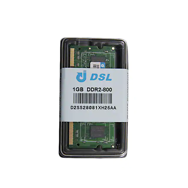
DDR2-800 1GB SO-DIMM 200PIN
With samsung 128Mx8 DRAM
D2SS28081XH25AA
Specifications
Density:
1GB
Data Rate:
800 Mbps
Version:
Unbuffered
CAS Latency:
6
Package:
SO-DIMM
Votage:
1.8V
Pin Count:
200pin
PCB Layers:
6
Speed:
PC2-6400
ECC :
Non ECC
Component Config:
128Meg x 8
Module Ranks :
Singel Rank
Features
Ʉġ All of Lead-Free products are compliant for ROHS
Ʉġ 200-pin,small outline,dual in-line memory module(SO-DIMM)
Ʉġ 1.8V + 0.1V power supply
Ʉġ Data rate:800Mbps(max)
Ʉġ 8 Banks
Ʉġ JEDEC standard 1.8V I/O(SSTL_18-compatible)
Ʉġ Burst Length: 4,8
Ʉġ /CAS Latency (CL):3,4,5,6
Ʉġ Double-data-rate architecture: two data transfers per clock cycle
Ʉġ Differential clock inputs (CK and /CK)
Ʉġ Four-bit prefetch architecture
Ʉġ Auto precharge operation for each burst access
Ʉġ Auto refresh and self refresh modes
Ʉġ Differential data strobe(DQS,DQS#) option
Ʉġ DLL to align DQ and DQS transitions with CK
Ʉġ Programmable Sequential / Interleave Burst Mode
Ʉġ Bi-directional Differential Data-Strobe (Single-ended data-strobe is an optional feature)
Ʉġ Posted CAS# additive latency (AL)
Ʉġ On Die Termination (ODT)
Ʉġ 64ms,8192-cycle refresh
Ʉġ Serial presence detect with EEPROM
Ʉġ Gold edge contacts
Ʉġ Average Refresh Period
7.8us at 0ɗ ʀTCASEʀ為85ɗ,
3.9us at為 85ɗ 烋TCASEʀ為95ɗ
1
REV 3.0
�DDR2-800 1GB SO-DIMM 200PIN
With samsung 128Mx8 DRAM
D2SS28081XH25AA
Description
The D2SS28081XH25AA is 128M words x 64 bits, 1 ranks DDRII SDRAM Small Outline Dual
In-line Memory Module, mounting 8 pieces of 1GB bits DDRII SDRAM sealed in FBGA(ȫBGA®)
package. Read and write operations are performed at the cross points of the CK and the /CK. This
high-speed data transfer is realized by the 4 bits prefetch-pipelined architecture. Data strobe (DQS
and /DQS) both for read and write are available for high speed and reliable data bus design. By
setting extended mode register, the on-chip Delay Locked Loop(DLL) can be set enable or disable.
This module provides high density mounting without utilizing surface mount technology. Decoupling
capacitors are mounted beside each FBGA(ȫBGA) on the module board.
ġ
Speed Grade & Key Parameters
DDR2-533
DDR2-667
CL3
400
400
CL4
533
533
533
Mbps
667
667
Mbps
800
Mbps
6-6-6
tCK
CL5
4-4-4
Unit
Mbps
CL6
CL-tRCD-tRP
DDR2-800
5-5-5
ġ
ġ
Speed Bins
Unit
DDR2-533
DDR2-667
DDR2-800
CL-tRCD-tRP
4-4-4
5-5-5
6-6-6
Parameter
min
min
min
CAS Latency
4
5
6
tCK
tRCD
15
15
15
ns
tRP
15
15
15
ns
tRAS
45
45
45
ns
tRC
60
60
60
ns
ġ
2
REV 3.0
�DDR2-800 1GB SO-DIMM 200PIN
With samsung 128Mx8 DRAM
D2SS28081XH25AA
Address Configuration
256MB
512MB
512MB
1GB
1GB
2GB
Dram Organization
32Mx16
64Mx8
64Mx16
64Mx8
128Mx8
128Mx8
Row address
A0~A12
A0~A13
A0~A12
A0~A13
A0~A13
A0~A13
Column address
A0~A9
A0~A9
A0~A9
A0~A9
A0~A9
A0~A9
Auto Precharge
A10
A10
A10
A10
A10
A10
Bank address
BA0~BA1
BA0~BA1
BA0~BA2
BA0~BA1
BA0~BA2
BA0~BA2
Refresh Method
8K/64ms
8K/64ms
8K/64ms
8K/64ms
8K/64ms
8K/64ms
4
8
4
16
8
16
# of DRAMs
Absolute Maximum Ratings
Symbol
Rating
Unit
Note
TCASE
0 to 95
ɗ
IJġ
Storage Temperature
TSTG
-50 to +100
ɗ
ġ
Storage Humidity
HSTG
5 to 95
%
Parameter
DRAM Component Case Temperature Range
Note:
1. If the DRAM case temperature is above 85ɗ炻the AUTO-Refresh command interval has to be reduced
to tREFI=3.9usˤ
DC Operating Conditions(SSTL_1.8)
Parameter
Symbol
Min
Typ.
Max
Unit
VDD
1.7
1.8
1.9
V
VDDL
1.7
1.8
1.9
V
VDDQ
1.7
1.8
1.9
V
Reference voltage
VREF
0.49*VDDQ
0.5*VDDQ
0.51*VDDQ
V
Termination voltage
VTT
VREF – 0.04
VREF
VREF +0.04
V
Input high voltage
VIH
VREF + 0.15
-
VREF + 0.30
V
EEPROM Supply Voltage
VDDSPD
1.7
-
3.6
V
DC input logic high
VIH(DC)
VREF+0.125
-
VDDQ+0.3
V
DC input low
VIL(DC)
-0.3
VREF-0.125
V
AC input logic high
VIH(AC)
VREF+0.250
-
-
V
AC input low
VIL(AC)
-
-
VREF-0.250
V
Supply Voltage
3
REV 3.0
�DDR2-800 1GB SO-DIMM 200PIN
With samsung 128Mx8 DRAM
D2SS28081XH25AA
Pin Description
Pin name
Description
Pin name
Description
A0~A13
DDR2 SDRAM address bus
CK0,CK1
Clock input
BA0,BA1
DDR2 SDRAM bank select
/CK0,/CK1
Differential clock input
/RAS
DDR2 SDRAM row address strobe
SCL
Clock input for serial PD
/CAS
DDR2 SDRAM column address strobe
SDA
Data input/output for serial PD
/WE
Wirte enable
S0,S1
SA0-SA1
DIMM Rank Select Lines
CKE0,CKE1
DDR2 SDRAM clock enable lines
ODT0,ODT1
On-die termination control lines
DQ0-DQ63
CB0-CB7
VDD*
VDDQ*
VREF
DIMM memory data bus
DIMM ECC check bits
VSS
VDDSPD
DQS0-DQS8 DDR2 SDRAM data strobes
DM(0-8)
NC
DDR2 SDRAM data masks
RESET
DQS0-DQS8 DDR2 SDRAM differential data strobes
TEST
Serial address input
DDR2 SDRAM core power supply
DDR2 SDRAM I/O Driver power supply
Input reference supply
Ground
Power for serial EEPROM
No connect
Not used on UDIMM
Unused on memory DIMMs
Pin Configuration
Pin
1
3
5
7
9
11
13
15
17
19
21
23
25
27
29
31
33
35
37
39
41
43
45
47
49
Front
VREF
VSS
DQ0
DQ1
VSS
DQS0
DQS0
VSS
DQ2
DQ3
VSS
DQ8
DQ9
VSS
DQS1
DQS1
VSS
DQ10
DQ11
VSS
VSS
DQ16
DQ17
VSS
DQS2
Pin
2
4
6
8
10
12
14
16
18
20
22
24
26
28
30
32
34
36
38
40
42
44
46
48
50
Back
VSS
DQ4
DQ5
VSS
DM0
VSS
DQ6
DQ7
VSS
DQ12
DQ13
VSS
DM1
VSS
CK0
CK0
VSS
DQ14
DQ15
VSS
VSS
DQ20
DQ21
VSS
NC
Pin
51
53
55
57
59
61
63
65
67
69
71
73
75
77
79
81
83
85
87
89
91
93
95
97
99
Front Pin Back Pin Front Pin Back Pin Front
DQS2 52
DM2 101
A1
102
A0
151 DQ42
VSS 103 VDD 104 VDD 153 DQ43
VSS
54
DQ18 56 DQ22 105 A10/AP 106 BA1 155 VSS
DQ19 58 DQ23 107 BA0 108 RAS 157 DQ48
VSS
VSS 109 WE 110
60
S0
159 DQ49
DQ24 62 DQ28 111 VDD 112 VDD 161 VSS
DQ25 64 DQ29 113 CAS 114 ODT0 163 NC,TEST
VSS
VSS 115 NC/S1 116 A13 165 VSS
66
DM3
68 DQS3 117 VDD 118 VDD 167 DQS6
NC
169 DQS6
NC
70 DQS3 119 NC/ODT1 120
VSS
VSS 121 VSS 122 VSS 171 VSS
72
DQ26 74 DQ30 123 DQ32 124 DQ36 173 DQ50
DQ27 76 DQ31 125 DQ33 126 DQ37 175 DQ51
VSS
VSS 127 VSS 128 VSS 177 VSS
78
CKE0 80 NC/CKE1 129 DQS4 130 DM4 179 DQ56
VDD
VDD 131 DQS4 132 VSS 181 DQ57
82
NC
84
NC
133
134 DQ38 183 VSS
VSS
BA2
86
NC
135 DQ34 136 DQ39 185 DM7
VDD
VDD 137 DQ35 138 VSS 187 VSS
88
A12
90
A11 139 VSS 140 DQ44 189 DQ58
A9
92
A7
141 DQ40 142 DQ45 191 DQ59
A8
94
A6
143 DQ41 144 VSS 193 VSS
VDD
VDD 145 VSS 146 DQS5 195 SDA
96
A5
98
A4
147 DM5 148 DQS5 197 SCL
A3
100
A2
149 VSS 150 VSS 199 VDDSPD
4
Pin
152
154
156
158
160
162
164
166
168
170
172
174
176
178
180
182
184
186
188
190
192
194
196
198
200
Back
DQ46
DQ47
VSS
DQ52
DQ53
VSS
CK1
CK1
VSS
DM6
VSS
DQ54
DQ55
VSS
DQ60
DQ61
VSS
DQS7
DQS7
VSS
DQ62
DQ63
VSS
SA0
SA1
REV 3.0
�DDR2-800 1GB SO-DIMM 200PIN
With samsung 128Mx8 DRAM
D2SS28081XH25AA
Input/Output Functional Description
Symbol
Type
Function
CK0-CK2
CK0-CK2
Input
CK and /CK are differential clock inputs. All the SDRAM addr/cntl inputs are sampled on the
crossing of positive edge of CK and negative edge of CK. Output (read) data is reference to the
crossing of CK and CK (Both directions of crossing)
CKE0-CKE1
Input
Activates the SDRAM CK signal when high and deactivates the CK Signal When low. By
deactivating the clock, CKE low initiates the Powe Down mode, or the Self-Refresh mode.
Input
Enables the associated SDRAM command decoder when low and disables the command
decoder when high. When the command decoder is disbled, new command are ignored but
previous operations continue. This signal provides for external rank selection on systems with
multiple ranks
Input
/RAS,/ CAS, and /WE(ALONG WITH CS) define the command being entered.
ODT0-ODT1
Input
When high, termination resistance is enabled for all DQ, /DQ and DM pins, assuming the
function is enabled in the Extended Mode Register Set (EMRS).
VREF
Supply
Reference voltage for SSTL 18 Inputs.
VDDQ
Supply
Power supply for the DDR II SDRAM output buffers to provide improved noise immunity. For all
current DDR 2 unbuffered DIMM designs, VDDQ shares the same power plane as VDD pins.
BA0-BA1
Input
Selects which SDRAM BANK of four is activated.
A0-A13
Input
During a Bank Activate command cycle, Address input defines the row address(RA0-RA13)
During a Read or Write command cycle. Address input defines the column address. In addition
to the column address. AP is used to invoke autoprecharge operation at the end of the burst
read or write cycle. If AP is high, autoprecharge is selected and BA0, BA1 defines the bank to be
precharged. If AP is low, autoprecharge is disbled. During a precharge command cycle, AP is
used in conjunction with BA0, BA1 to control which bank(s) to precharge. If AP is high, all banks
will be precharged regardless of the state of BA0, BA1. If AP is low, BA0, BA1 are used to define
which bank to precharge.
DQ0-DQ63
CB0-CB7
In/Out
Data and Check Bit Input/Output pins.
DM0-DM8
Input
DM is and input mask signal for write data. Input data is masked when DM is sampled High
coincident with that input data during a write access. DM is sampled on both edges of DQS.
Although DM pins are input only, the DM loading matches the DQ and DQS loading.
VDD, VSS
Supply
Power and ground for DDR2 SDRAM input buffers, and core logic. VDD and VDDQ pins are tied
to VDD/VDDQ planes on these modules.
DQS0-DQS8
DQS0-DQS8
In/Out
Data strobe for input and output data. For Rawcards using x16 organized DRAMs DQ0-7
connect to the LDQS pin of the DRAMs and DQ8-17 connect to the UDQS pin of the DRAM
SA0-SA2
Input
These signals and tied at the system planar to either VSS or VDD to configure the serial SPD
EERPOM address range.
SDA
In/Out
This bi-directional pin is used to transfer data into or out of the SPD EEPROM. A resistor must
be connected from the SDA bus line to VDD to act as a pullup on the system board.
SCL
Input
This signal is used to clock data into and out of the SPD EEPROM. A resistor may be connected
from the SCL bus time to VDD to act as a pullup on the system board.
VDD SPD
Supply
Power supply for SPD EEPROM. This supply is separate from the VDD/VDDQ power plane.
EEPROM supply is operable from 1.7V to 3.6V.
/S0-/S1
/RAS,/CAS,/WE
5
REV 3.0
�DDR2-800 1GB SO-DIMM 200PIN
With samsung 128Mx8 DRAM
D2SS28081XH25AA
FUNCTIONAL BLOCK DIAGRAM
6
REV 3.0
�DDR2-800 1GB SO-DIMM 200PIN
With samsung 128Mx8 DRAM
D2SS28081XH25AA
Timing Parameters by Speed Grade
7
REV 3.0
�DDR2-800 1GB SO-DIMM 200PIN
With samsung 128Mx8 DRAM
D2SS28081XH25AA
8
REV 3.0
�DDR2-800 1GB SO-DIMM 200PIN
With samsung 128Mx8 DRAM
D2SS28081XH25AA
SERIAL PRESENCE DETECT
Byte No.
Function Described
Function Supported
Hex Value
0
# of Serial PD Bytes written during module production
128 Bytes
80
1
Total number of Bytes in SPD device
256 Bytes
08
2
Fundameatal memory type
DDR2 SDRAM
08
3
# of row address on this assembly
14
0E
4
# of column address on this assembly
10
0A
5
# of module rows on this assembly
1 rank
60
6
Data width of this assembly
64bits
40
7
Reserved
--
00
8
Voltage interface level of this assembly
SSTL 1.8V
05
9
DDR2 SDRAM cycle time at Max. Supported CAS latency=X
2.5ns
25
10
DDR2 SDRAM Access time from clock at CL=X
4.0ns
40
11
DIMM configuration type(address&command parity, data parity,ECC)
Non parity/ECC
00
12
Refresh rate
7.8us
82
13
Primary DDR2 SDRAM width
X8
08
14
Error checking DDR2 SDRAM width
N/A
00
15
Reserved
--
00
16
DDR2 SDRAM device attributes:Burst lengths supported
4,8
0C
4
08
4,6,6
70
DDR2 SDRAM device attributes:# of banks on each DDR2 SDRAM
17
Device
18
DDR2 SDRAM device attributes: CAS latency supported
19
Reservedġ
20
DIMM type information
21
DDR2 SDRAM module attributes
22
DDR2 SDRAM device attributes : General
23
01
SO-DIMM
04
--
00
50ohm ODT
07
DDR2 SDRAM cycle time at CL = X-1
3.75ns
30
24
DDR2 SDRAM access time from clock at CL = X-1
0.45ns
45
25
DDR2 SDRAM cycle time at CL = X-2
3.75ns
3D
26
DDR2 SDRAM access time from clock at CL = X-2
0.5ns
50
27
Minimum row precharge time(=tRP)
15ns
3C
28
Minimum row active to row active delay(=tRRD)
7.5ns
1E
29
Minimum RAS to CAS delay(=tRCD)
15ns
32
30
Minimum active precharge time(=tRAS)
45ns
2D
9
REV 3.0
�DDR2-800 1GB SO-DIMM 200PIN
With samsung 128Mx8 DRAM
D2SS28081XH25AA
Byte No.
Function Described
31
Module rank density
32
Function Supported
Hex Value
1GB
01
Command and address setup time before clock(=tIS)
0.17ns
17
33
Command and address hold time after clock(=tIH)
0.25ns
25
34
Data input setup time before strobe(=tDS)
0.05ns
05
35
Data input hold time after strobe(=tDH)
0.12ns
12
36
Write recovery time (tWR)
15ns
3C
37
Write to read CMD delay (tWTR)
7.5ns
1E
38
Read to precharge CMD delay (tRTP)
7.5ns
1E
39
Mem analysis probe
TBD
00
40
Extension of byte 41 and 42
41
Active command period (tRC)
60ns
3C
42
Auto refresh to active/ Auto refresh command cycle (tRFC)
105ns
7F
43
SDRAM tCK cycle max (tCK max)
8ns
80
44
Dout to DQS skew
0.20ns
14
45
Data hold skew (tQHS)
0.30ns
1E
46
PLL relock time
Undefined
00
--
--
Revision 1.0
12
E2
47 to 61
Undefined
Reserved
62
SPD data revision code
63
Checksum for Bytes 0~ 62
--
64 to 94
Manufacturer JEDEC ID code
--
95 to 98
Assembly serial #
--
99 to 127
Manufacturer specific data(may be used in future)
Undefined
128 to 225
Open for customer use
Undefined
10
06
REV 3.0
�DDR2-800 1GB SO-DIMM 200PIN
With samsung 128Mx8 DRAM
D2SS28081XH25AA
PACKAGE DIMENSIONS
Unit:mm
67.60Ʋ0.15mm
The used device is SAMSUNG, 128M x 8 ,FBGA
DDR2 SDRAM Part No.: K4T1G084QG-BCF7 *8EA
11
REV 3.0
�DDR2-800 1GB SO-DIMM 200PIN
With samsung 128Mx8 DRAM
D2SS28081XH25AA
Declaration of Compliance with the RoHS Directive
DATA SPECIALTIES CO.,LTD. Hereby declares that the products compliant with the European Union
Directive 2002/95/EC for Restriction of the use of certain Hazardous Substances in Electrical and Electronic
Equipment(RoHS Directive).
Below list of DSL(DATA SPECIALTIES CO.,LTD.) products are Compliance.
No.
Substance
Max. Conc.
1
Cd (Cadmium)