Specification
Part No.
:
WLA.01
Model
:
2.4GHz High Efficiency Loop Antenna
Description
:
2.5dBi 2400MHz to 2500MHz
WLAN/WIFI/Bluetooth/Zigbee
Features
:
3.2*1.6*0.5mm
Low Profile
Peak gain 2.5dBi
50 Ohm Impedance
RoHS Compliant
SPE-11-8-146/K/SS
Page 1 of 18
�1. Introduction
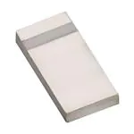
The WLA.01 2.4GHz Loop antenna is a high efficiency, miniature SMD, edge mounted ceramic
antenna for very small space requirements for Wi-Fi, WLAN, Zigbee, Bluetooth, and 802.11
applications. The WLA.01 uses the main PCB as its ground plane, thereby increasing Antenna
Efficiency. It is tuned for different PCB sizes by simply changing the value of the matching
circuit. At 3.2mm*1.6mm*0.5mm, the WLA.01 is one of the smallest antennas available
worldwide. This antenna is delivered on tape and Reel.
Many module manufacturers specify peak gain limits for any antennas that are to be
connected to that module. Those peak gain limits are based on free-space conditions. In
practice, the peak gain of an antenna tested in free-space can degrade by at least 1 or 2dBi
when put inside a device. So ideally you should go for a slightly higher peak gain antenna than
mentioned on the module specification to compensate for this effect, giving you better
performance.
Upon testing of any of our antennas with your device and a selection of appropriate layout,
integration technique, or cable, Taoglas can make sure any of our antennas’ peak gain will be
below the peak gain limits. Taoglas can then issue a specification and/or report for the
selected antenna in your device that will clearly show it complying with the peak gain limits,
so you can be assured you are meeting regulatory requirements for that module.
For example, a module manufacturer may state that the antenna must have less than 2dBi
peak gain, but you don’t need to select an embedded antenna that has a peak gain of less
than 2dBi in free-space. This will give you a less optimized solution. It is better to go for a
slightly higher free-space peak gain of 3dBi or more if available. Once that antenna gets
integrated into your device, performance will degrade below this 2dBi peak gain due to the
effects of GND plane, surrounding components, and device housing. If you want to be
absolutely sure, contact Taoglas and we will test. Choosing a Taoglas antenna with a higher
peak gain than what is specified by the module manufacturer and enlisting our help will
ensure you are getting the best performance possible without exceeding the peak gain limits.
SPE-11-8-146/K/SS
Page 2 of 18
�1.1 Applications
*Bluetooth earphone systems
*Hand-held devices when Bluetooth/Wi-Fi functions are needed, e.g., Smart phone.
*IEEE802.11 b/g
*ZigBee
*Wireless PCMCIA cards or USB dongle
SPE-11-8-146/K/SS
Page 3 of 18
�2. Specifications
The WLA.01 is designed to mount at the center of the edge of an evaluation board of 80 x
40mm.The antenna performance was measured with the WLA.01 mounted on the evaluation
board with SMA(F) connector.
No
Parameter
Specification*
1
Center Frequency
2400-2500MHz
2
Dimensions
3.2*1.6*0.5mm
3
VSWR
2 max
4
Polarization
Linear
5
Bandwidth
100MHz min.
6
Gain
Peak 2.5dBi typ.
7
Efficiency
84% typ.
8
Impedance
50
Mechanical
9
10
Dimensions
3.2*1.6*0.5mm
Material
Ceramic
Environmental
11
Operating Temperature
-40°C+85°C
12
Storage Temperature
-40°C+105°C
13
Temperature Coefficient(τf)
0 20 ppm @-20ºC to +80ºC
Recommended Reel Storage
5°C to 40°C
Condition
Relative Humidity 20% to 70%
14
* The data was measured by a CTIA Authorized Test Lab.
** Center frequency will be offset to working frequency according to the conditions of
user’s Ground plane and radome.
SPE-11-8-146/K/SS
Page 4 of 18
�3. Electrical Specification
(80*40mm ground plane)
3.1 Return Loss(S11)
SPE-11-8-146/K/SS
Page 5 of 18
�3.2 VSWR
SPE-11-8-146/K/SS
Page 6 of 18
�4. Radiation Pattern (Customize Design)
SPE-11-8-146/K/SS
Page 7 of 18
�4.1 Radiation Pattern (80mmX40mm ground plane)
Z
X
Y
4.2 3D Gain pattern @2442MHz
SPE-11-8-146/K/SS
Page 8 of 18
�SPE-11-8-146/K/SS
Page 9 of 18
�4.3 Efficiency Table
4.4 Efficiency vs Frequency
SPE-11-8-146/K/SS
Page 10 of 18
�5. Layout Guide
5.1 Solder Land Pattern
Land pattern for soldering (grey marking areas) is as shown below. A matching circuit
similar to the one shown in section 5.3 is also required.
SPE-11-8-146/K/SS
Page 11 of 18
�SPE-11-8-146/K/SS
Page 12 of 18
�5.2 Solder Land Pattern
This antenna includes a fine tuning element (as shown in the land patterns above)
that can be used to slightly shift antenna resonance.
5.3 Matching Circuit
Like all antennas, surrounding components, enclosures, and changes to the GND
plane dimensions can alter performance. A pi-matching network like the one shown
below is required in case adjustments need to be made. The antenna EVB has a similar
matching network. The components on the EVB are a good starting point for a new
design, but will need to be adjusted upon integration for best performance. The zero
ohm resistor is needed for the ability to solder down a coax pigtail to make
measurements with a vector network analyzer.
SPE-11-8-146/K/SS
Page 13 of 18
�6. Antenna Drawings
6.1 Antenna Main Body
SPE-11-8-146/K/SS
Page 14 of 18
�6.2 Antenna with EVB
6.3 Footprint on EVB
SPE-11-8-146/K/SS
Page 15 of 18
�7. Packaging
SPE-11-8-146/K/SS
Page 16 of 18
�7.1 Tape Dimensions (unit: mm)
Feature
Specifications
Tolerances
W
12
±0.30
P
8
±0.10
E
1.75
±0.10
F
5.5
±0.10
P2
2
±0.10
D
1.5
±0.10
Po
4
±0.10
10Po
40
±0.20
7.2 Pocket Dimensions (unit: mm)
Feature
Specifications
Tolerances
Ao
1.9
±0.10
Bo
3.5
±0.10
Ko
0.8
±0.10
t
0.3
±0.05
SPE-11-8-146/K/SS
Page 17 of 18
�8. Recommended Reflow Temp Profile
The WLA.01 Loop Antenna can be assembled following either Sn-Pb or Pb-Free assembly
processes. The recommended soldering temperatures are as follows:
SPE-11-8-146/K/SS
Page 18 of 18
�
很抱歉,暂时无法提供与“WLA.01”相匹配的价格&库存,您可以联系我们找货
免费人工找货- 国内价格 香港价格
- 5000+6.840535000+0.88609
- 10000+6.7111410000+0.86933