SPECIFICATION
Part No.
:
CA.25
Product Name
:
2.4/5 GHz Dual-Band Wi-Fi Dielectric Loop Antenna
Feature
:
Smallest 2400MHz to 2500MHz/5150MHz to 5850MHz
Dual-Band SMT Type Antenna
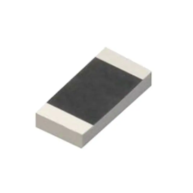
Ultra Low profile 3.05mm x 1.6mm x 0.55mm
Supports IEEE 802.11 a/b/g/n and ac Dual-Band WIFI
systems
Linear Polarization
Tuned on 40*80mm ground plane
RoHS Compliant
SPE-15-8-005/B/WY
Page 1 of 24
�1. Introduction
The CA.25 is a super small SMT ceramic loop antenna for 2400MHz to
2500MHz/ 5150MHz to 5850MHz dual band that includes Bluetooth, WIFI,
Zigbee, and ISM applications. The CA.25 has a peak gain of 1.0 dBi and 1.5
dBi at 2.4GHz and 5.5GHz, respectively, with an efficiency of at least 60%.
This antenna is delivered on tape and reel.
The CA.25 antenna has an ultra-low profile form factor of 3.05mm x 1.6mm x
0.55mm and allows use on extremely thin devices while still maintaining
excellent RF performance characteristics. All that is needed is a 50 Ohm
transmission line to the module.
Typical applications include:
USB dongles
Tablets
Home and industrial in-wall WIFI automation
Hand-held devices
Many module manufacturers specify peak gain limits for any antennas that are
to be connected to that module. Those peak gain limits are based on freespace conditions. In practice, the peak gain of an antenna tested in free-space
can degrade by at least 1 or 2dBi when put inside a device. So ideally you
should go for a slightly higher peak gain antenna than mentioned on the
module specification to compensate for this effect, giving you better
performance.
Upon testing of any of our antennas with your device and a selection of
appropriate layout, integration technique, or cable, Taoglas can make sure any
SPE-15-8-005/B/WY
Page 2 of 24
�of our antennas’ peak gain will be below the peak gain limits. Taoglas can then
issue a specification and/or report for the selected antenna in your device that
will clearly show it complying with the peak gain limits, so you can be assured
you are meeting regulatory requirements for that module.
For example, a module manufacturer may state that the antenna must have
less than 2dBi peak gain, but you don’t need to select an embedded antenna
that has a peak gain of less than 2dBi in free-space. This will give you a less
optimized solution. It is better to go for a slightly higher free-space peak gain
of 3dBi or more if available. Once that antenna gets integrated into your device,
performance will degrade below this 2dBi peak gain due to the effects of GND
plane, surrounding components, and device housing. If you want to be
absolutely sure, contact Taoglas and we will test. Choosing a Taoglas antenna
with a higher peak gain than what is specified by the module manufacturer
and enlisting our help will ensure you are getting the best performance
possible without exceeding the peak gain limits.
Custom tuned versions for different ground-planes and housing environments
can be made subject to a minimum order quantity.
Contact your regional Taoglas sales office for support to integrate and test this
antenna performance in your device.
CA.25 also has GPS/Glonass/Beidou functionality, if client follows our specific
matching circuit components on their main board, it can be re-tuned to work
as an embedded GNSS antenna. Please kindly refer to our specification
AGGBLA.03.07.0095A.
SPE-15-8-005/B/WY
Page 3 of 24
�2. Specification Table
Parameter
Working Frequency
Specification
2400~2500 MHz
5150~5850 MHz
VSWR
3.0
3.0
Peak Gain
0.5 dBi
3.3 dBi
Efficiency(Peak)
60%
70%
Polarization
Linear
Impedance
50 Ohm
Weight
9mg
Dimensions
3.05 x 1.6 x 0.55 mm
Operating Temperature
-40 to +85C
* These values are based on our standard 40mmx80mm test board. Actual
electrical values will change depending on ground plane size, shape, mounting
position, matching circuit design, and surrounding environment.
SPE-15-8-005/B/WY
Page 4 of 24
�3. Test Setup
Y
X
Z
SPE-15-8-005/B/WY
Page 5 of 24
�4. Electrical Specifications
4.1 Return Loss
Return
Loss
S11(dB)
2400MHz
2450MHz
2500MHZ
5150MHz
5550MHz
5850MHz
-6.0
-11.0
-9.5
-9.1
-15.9
-11.6
SPE-15-8-005/B/WY
Page 6 of 24
�4.2 Efficiency
WLAN
2400MHz
2450MHz
2500MHZ
5150MHz
5550MHz
5850MHz
Efficiency
32.30%
56.37%
59.48%
49.10%
61.01%
49.10%
SPE-15-8-005/B/WY
Page 7 of 24
�4.3 Average Gain
WLAN
Average
(dBi)
2400MHz
2450MHz
2500MHZ
5150MHz
5550MHz
5850MHz
-4.90
-2.48
-2.25
-3.08
-1.93
-3.08
SPE-15-8-005/B/WY
Page 8 of 24
�4.4 Peak Gain
WLAN
2400MHz
2450MHz
2500MHZ
5150MHz
5550MHz
5850MHz
Peak (dBi)
-1.39
0.47
0.59
0.96
2.64
2.07
SPE-15-8-005/B/WY
Page 9 of 24
�4.5 2D Radiation Pattern
XY-Plane
X
0
330
5
30
-5
-15
300
60
-25
-35
270
90 Y
-45
2400MHz
240
120
210
2450MHz
150
2500MHz
(dBi)
180
X
0
330
5
30
-5
-15
300
60
-25
-35
270
90
-45
Y
4900MHz
5150MHz
240
120
5350MHz
5650MHz
210
150
180
5750MHz
(dBi)
5850MHz
SPE-15-8-005/B/WY
Page 10 of 24
�XZ-Plane
Z
0
330
5
30
-5
-15
300
60
-25
-35
270
90 X
-45
2400MHz
240
120
2450MHz
210
150
180
2500MHz
(dBi)
Z
0
330
5
30
-5
-15
300
60
-25
-35
270
90
-45
X
4900MHz
5150MHz
240
120
5350MHz
5650MHz
210
150
180
5750MHz
(dBi)
5850MHz
SPE-15-8-005/B/WY
Page 11 of 24
�YZ-Plane
Z
0
330
5
30
-5
-15
300
60
-25
-35
270
90 Y
-45
2400MHz
240
120
2450MHz
210
150
180
2500MHz
(dBi)
Z
0
330
5
30
-5
-15
300
60
-25
-35
270
90
-45
Y
4900MHz
5150MHz
240
120
210
5350MHz
5650MHz
150
5750MHz
180
(dBi)
5850MHz
SPE-15-8-005/B/WY
Page 12 of 24
�4.6 3D Radiation Pattern
2450MHz
SPE-15-8-005/B/WY
Page 13 of 24
�5. Footprint Layout Guide
5.1 Top Copper
SPE-15-8-005/B/WY
Page 14 of 24
�5.2 Top Solder Paste
SPE-15-8-005/B/WY
Page 15 of 24
�5.3 Top Solder Mask
SPE-15-8-005/B/WY
Page 16 of 24
�5.4 Composite Diagram
SPE-15-8-005/B/WY
Page 17 of 24
�5.5 Matching Circuit
Like all antennas, surrounding components, enclosures, and changes to the
GND plane dimensions can alter performance. A pi-matching network like the
one shown below is required in case adjustments need to be made. The
antenna EVB has a similar matching network. The components on the EVB
are a good starting point for a new design, but will need to be adjusted upon
integration for best performance. The zero ohm resistor is needed for the
ability to solder down a coax pigtail to make measurements with a vector
network analyzer.
Antenna
0 Ohm
Resistor
S1
Transmission Line
S3
S2
SPE-15-8-005/B/WY
Page 18 of 24
�6. Antenna Drawings
6.1 Antenna Dimension
SPE-15-8-005/B/WY
Page 19 of 24
�6.2 Antenna with Evaluation Board
SPE-15-8-005/B/WY
Page 20 of 24
�6.3 Footprint on Evaluation Board
SPE-15-8-005/B/WY
Page 21 of 24
�7. Packing
(1) Blister tape to IEC 286-3,polyester.
(2) Pieces /tape:5000 pcs (Vacuum packing).
(3) Pieces /Carton-Inside:10000 pcs.
(4) Pieces /Carton-Outside:50000 pcs.
SPE-15-8-005/B/WY
Page 22 of 24
�8. Recommended Reflow Soldering Profile
The CA.25 loop antenna can be assembled following Pb-free assembly.
According to the Standard IPC/JEDEC J-STD-020C, the temperature profile
suggested is shown below:
Phase
PREHEAT
RAMP-UP
Profile features
Pb-Free Assembly(SnAgCu)
Temperature Min(Tsmin)
150℃
Temperature Max(Tsmax)
200℃
Time(ts) from(Tsmin to Tsmax)
60-120 seconds
Avg. Ramp-up Rate(Tsmax to
TP)
REFLOW
PEAK
RAMP-DOWN
3℃ / second(max)
Temperature(TL)
217℃
Total Time above TL(t L)
30-100 seconds
Temperature(TL)
260℃
Time(tp)
5-10 second
Rate
6℃ / second max.
Time from 25℃ to Peal Temperature
8 minutes max.
Composition of solder paste
96.5Sn/3Ag/0.5Cu
Solder Paste Model
SHENMAO PF606-P26
Note: Temperature measurement point is on top surface of the component.
Damage can result if recommended temperature is exceeded.
SPE-15-8-005/B/WY
Page 23 of 24
�Soldering condition : Soldering iron temperature 270±10 ℃.
Apply preheating at 120℃for 2-3 minutes. Finish soldering for each terminal
within 3 seconds, if soldering iron over temperature 270±10 ℃ for 3 seconds,
component surface peeling or damage may occur.
Soldering iron cannot dissipate electricity.
SPE-15-8-005/B/WY
Page 24 of 24
�
很抱歉,暂时无法提供与“CA.25”相匹配的价格&库存,您可以联系我们找货
免费人工找货