KH3 Series
Receiver Module
Data Guide
�! Warning: Some customers may want Linx radio frequency (“RF”)
products to control machinery or devices remotely, including machinery
or devices that can cause death, bodily injuries, and/or property
damage if improperly or inadvertently triggered, particularly in industrial
settings or other applications implicating life-safety concerns (“Life and
Property Safety Situations”).
Table of Contents
1^
1^
1^
NO OEM LINX REMOTE CONTROL OR FUNCTION MODULE
SHOULD EVER BE USED IN LIFE AND PROPERTY SAFETY
SITUATIONS. No OEM Linx Remote Control or Function Module
should be modified for Life and Property Safety Situations. Such
modification cannot provide sufficient safety and will void the product’s
regulatory certification and warranty.
2^
Customers may use our (non-Function) Modules, Antenna and
Connectors as part of other systems in Life Safety Situations, but
only with necessary and industry appropriate redundancies and
in compliance with applicable safety standards, including without
limitation, ANSI and NFPA standards. It is solely the responsibility of any
Linx customer who uses one or more of these products to incorporate
appropriate redundancies and safety standards for the Life and
Property Safety Situation application.
7^
Do not use this or any Linx product to trigger an action directly
from the data line or RSSI lines without a protocol or encoder/
decoder to validate the data. Without validation, any signal from
another unrelated transmitter in the environment received by the module
could inadvertently trigger the action.
All RF products are susceptible to RF interference that can prevent
communication. RF products without frequency agility or hopping
implemented are more subject to interference. This module does not
have a frequency hopping protocol built in.
Do not use any Linx product over the limits in this data guide.
Excessive voltage or extended operation at the maximum voltage could
cause product failure. Exceeding the reflow temperature profile could
cause product failure which is not immediately evident.
Do not make any physical or electrical modifications to any Linx
product. This will void the warranty and regulatory and UL certifications
and may cause product failure which is not immediately evident.
2^
3^
5^
6^
8^
8^
9^
10^
10^
10^
11^
11^
12^
13^
14^
16^
17^
18^
19^
19^
21^
22^
22^
22^
Description
Features
Applications
Ordering Information
Absolute Maximum Ratings
Electrical Specifications
Typical Performance Graphs
Pin Assignments
Pin Descriptions
Module Description
Theory of Operation
Decoder Operation
Compatibility with the KH2 Series
Setting the Receiver Address
The Data Line Outputs
Receiving Data
Using the RSSI Line
Input Type Selection
Power Supply Requirements
Typical Applications
Antenna Considerations
Helpful Application Notes from Linx
Interference Considerations
Pad Layout
Board Layout Guidelines
Microstrip Details
Production Guidelines
Hand Assembly
Automated Assembly
� 24^
General Antenna Rules
26^ Common Antenna Styles
28^ Regulatory Considerations
30^ Notes
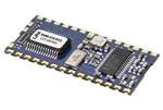
KH3 Series Receiver Module
Data Guide
Description
1.43 in
The KH3 Series is ideally suited for volume
(36.32 mm)
use in OEM applications such as remote
0.63 in
control / command and keyless entry. It (16.00 mm)
combines a high-performance RF receiver
with an on-board decoder. When paired
0.106 in
with a matching KH3 Series transmitter /
encoder module, OEM transmitter, or LC (2.69 mm)
or LR Series transmitter and DS Series
Figure 1: Package Dimensions
encoder combination, a highly reliable
wireless link is formed that is capable of transferring the status of eight
parallel inputs for distances of up to 3,000 feet (1,000m). Ten address
lines provide 1,022 (210-2) different addresses for security and uniqueness.
Housed in a compact SMD package, the KH3 module utilizes an advanced
synthesized architecture to achieve an unmatched blend of performance,
size, range and cost. No external RF components are required except an
antenna, making design integration straightforward.
Features
•
•
•
•
•
•
•
•
Low cost
Long range
On-board encoder
8 parallel binary inputs
210 addresses for uniqueness
Ultra-low power consumption
Compact SMD package
Advanced synthesized
architecture
Received data output
Transmission validation
No production tuning
No external RF components
required (except an antenna)
• Pin-compatible with original KH
and KH2 modules
•
•
•
•
Applications
•
•
•
•
Remote control / command
Gate openers
Lighting control
Call systems
•
•
•
– 1 –
Remote status monitoring
Home / industrial automation
Wire elimination
Revised 3/18/2015
�Ordering Information
Electrical Specifications
Ordering Information
KH3 Series Receiver Specifications
Part Number
Description
Parameter
TXM-315-KH3
315MHz Transmitter / Encoder
Power Supply
TXM-418-KH3
418MHz Transmitter / Encoder
Operating Voltage
TXM-433-KH3
433MHz Transmitter / Encoder
RXM-315-KH3
315MHz Receiver / Decoder
RXM-418-KH3
RXM-433-KH3
EVAL-***-KH3
Symbol
Min.
Typ.
Max.
Units
VCC
2.7
3.0
3.6
VDC
5.2
VDC
1,4
Supply Current
lCC
4.0
5.9
7.0
mA
7
418MHz Receiver / Decoder
Power Down Current
lPDN
47
57
µA
4
433MHz Receiver / Decoder
Receiver Section
KH3 Series Basic Evaluation Kit
Receive Frequency Range
With Dropping Resistor
*** = 315, 418 (Standard), 433MHz
Receivers are supplied in tubes of 20 pcs.
FC
RXM-315-KH3
315
MHz
RXM-418-KH3
418
MHz
RXM-433-KH3
Figure 2: Ordering Information
433.92
Center Frequency Accuracy
–50
LO Feedthrough
Absolute Maximum Ratings
IF Frequency
Noise Bandwidth
Absolute Maximum Ratings
Supply Voltage Vcc
−0.3
to
+3.6
VDC
Any Input or Output Pin
−0.3
to
+3.6
VDC
RF Input
0
dBm
Operating Temperature
−40
to
+70
ºC
Storage Temperature
−55
to
+85
ºC
Soldering Temperature
+255ºC for 10 seconds
Exceeding any of the limits of this section may lead to permanent damage to the device.
Furthermore, extended operation at these maximum ratings may reduce the life of this
device.
– 2 –
kHz
–80
dBm
2,4
10.7
MHz
5
N3DB
280
kHz
Data Rate
100
10,000
bps
Data Output
Logic Low
VOL
0.0
VDC
3
Logic High
VOH
3.0
VDC
3
Power-Down Input
Logic Low
VIL
Logic High
VIH
Receiver Sensitivity
0.4
VCC–0.4
–106
VDC
VDC
–112
–118
dBm
RSSI / Analog
80
Analog Bandwidth
Warning: This product incorporates numerous static-sensitive
components. Always wear an ESD wrist strap and observe proper ESD
handling procedures when working with this device. Failure to observe
this precaution may result in module damage or failure.
MHz
+50
FIF
Dynamic Range
Figure 3: Absolute Maximum Ratings
Notes
50
5,000
dB
4
Hz
4
Gain
16
mV/dB
4
Voltage With No Carrier
1.5
V
4
50
Ω
4
Antenna Port
RF Input Impedance
RIN
Timing
Receiver Turn-On Time
Via VCC
3.0
7.0
10.0
ms
4,5
Via PDN
0.04
0.25
0.50
ms
4,5
– 3 –
�Typical Performance Graphs
KH2 Series Receiver Specifications Continued
Parameter
Symbol
Min.
Typ.
Max.
Units
Notes
1.2
mA
6
+70
°C
4
1V/div
2.00ms/div
A
∆A-B = 4.2109 ms
B
Decoder Section
TX Data Length
26 bits
3x
Average Data Duty Cycle
50%
Output Drive Current
0.6
1.0
Environmental
Operating Temperature
Range
1.
2.
3.
–40
The KH3 can utilize up to a 5.2VDC
supply provided a dropping resistor is
placed in series with VCC. However, it
is recommended to use a 3.0 - 3.3V
supply.
Into a 50Ω load
When operating from a 5V source, it is
important to consider that the output
will swing to well less than 5 volts
as a result of the required dropping
resistor. Please verify that the minimum
voltage will meet the high threshold
requirement of the device to which data
is being sent.
4.
5.
6.
7.
Characterized, but not tested
Time to valid data output
Maximum drive capability of data
outputs
At 25°C
Figure 5: KH3 Series Receiver Turn-On Time from VCC
1V/div
A
100µs/div
∆A-B = 101.83 µs
B
Figure 4: Electrical Specifications
Figure 6: KH3 Series Receiver Turn-On Time from PDN
6.60
85°C
RX Current (mA)
6.40
25°C
6.20
-40°C
6.00
5.80
5.60
5.40
2.7
2.8
2.9
3
3.1
3.2
3.3
Input Voltage (V)
Figure 7: KH3 Series Receiver Current Consumption vs. Supply Voltage
– 4 –
– 5 –
3.4
3.5
3.6
�Pin Descriptions
2.20
RSSI Voltage (V)
2.00
Pin Descriptions
Pin Number
Name
I/O
Description
1
NC
—
No Connection. For physical support only.
1.60
2, 3, 7, 8, 9,
12, 13, 14
D0–D7
O
Data Output Lines. Upon a valid transmission, these
lines are set to replicate the state of the transmitter’s
data lines.
1.40
4
GND
—
Analog Ground
5
VCC
—
Supply Voltage
6
PDN
I
Power Down. Pulling this line low places the receiver
into a low-current state. The module is not able to
receive a signal in this state.
10
DATA
O
Data output of the receiver prior to the decoder.
11
VT
O
Valid Transmission. This line goes high when a valid
transmission is received.
15–24
A0–A9
I
Address Lines. The state of these lines must match
the state of the transmitter’s address lines in order for
a transmission to be accepted. These lines are pulled
to VCC internally.
25
RSSI
26
1.80
1.20
-100
-90
-80
-70
-60
-50
-40
-30
-20
-10
0
Input Power (dBm)
Figure 8: KH3 Series Receiver RSSI Response Time
Pin Assignments
28
2
D0
GND
27
3
D1
NC
26
4
GND
RSSI
25
5
VCC
A9
24
6
PDN
A8
23
7
D2
A7
22
8
D3
A6
21
9
D4
A5
20
10
DATA
A4
19
11
VT
A3
18
12
D5
A2
17
13
D6
A1
16
14
D7
A0
15
29 30
A_CFG1
ANT
A_CFG0
NC
D_CFG
1
O
Received Signal Strength Indicator. This line outputs
an analog voltage that is proportional to the strength
of the received signal.
NC
—
No Connection. For physical support only.
27
GND
—
Analog Ground
28
RF IN
I
50-ohm RF Input
29
D_CFG
I
Data Line Configuration. Determines whether a low
on a data line is interpreted as a zero bit or an open
bit. See the Input Type Selection section. This line is
pulled to GND internally.
30, 31
A_CFG0
I
Address Configuration 0. With A_CFG1, determines
the address bit type interpretation. See the Input Type
Selection section. This line is pulled to GND internally.
31
A_CFG1
I
Address Configuration 1. With A_CFG0, determines
the address bit type interpretation. See the Input Type
Selection section. This line is pulled to VCC internally.
Figure 10: KH3 Series Receiver Pin Descriptions
31
Figure 9: KH3 Series Receiver Pinout (Top View)
– 6 –
– 7 –
�Module Description
Decoder Operation
The KH3 Series module combines the popular Linx LR Series receiver
with a decoder IC in a convenient SMD package. The module is ideal for
general-purpose remote control and command applications. When paired
with a matching Linx KH3 Series transmitter / encoder, OEM transmitter,
LC, or LR Series transmitter and DS Series encoder combination, a highly
reliable RF link is formed, capable of transferring control and command
data over line-of-sight distances in excess of 3,000 feet. The on-board
receiver / decoder combination provides eight switched outputs that
correspond to the state of the data lines on the transmitter’s encoder.
Ten address lines are also provided to allow up to 1,022 (210 - 2) unique
identification codes.
The KH3 Series receiver utilizes the
DS Series decoder. When the decoder
receives data, it compares the address in
the received packet to its local address
lines. If the addresses match, then the
data is stored and a second packet is
received. The decoder compares the
two packets to each other. If the packets
match, then the received data bits are
output on the data lines and the VT line
is pulled high. It then looks for the next
packet.
RF Stage
Decoder Stage
Address Inputs
A0-A9
50Ω RF IN
(Antenna)
10.7MHz
IF Filter
0°
LNA
Data Slicer
-
Σ
Band Select
Filter
90°
PLL
Limiter
VT
Data In
+
RSSI
Parallel
Outputs
D0-D7
VCO
Power On
Sleep
Wake on interrupt
Once no valid data is received (there is
a mismatch of address, of data, or of bit
timings), the data and VT lines are pulled
low and the decoder goes to sleep until
more data is received.
NO
Data
received?
YES
NO
Valid data
received?
YES
NO
Address
match?
YES
NO
1st valid
packet?
YES
2nd packet
received?
YES
D_CFG
D_CFG0
D_CFG1
XTAL
Figure 11: KH3 Series Receiver Block Diagram
Theory of Operation
The KH3 Series receiver module is designed to receive transmissions
from a matching KH3 Series transmitter module or other compatible
Linx transmitter product. When transmitted data is received, the data is
presented to the onboard decoder. If the incoming address matches the
local address settings, the decoder’s outputs are set to replicate the states
of the transmitter’s data lines.
The RF section of the KH3 module utilizes the LR Series receiver, which
is an advanced single-conversion superhet design with a synthesized
architecture, high IF frequency, and multilayer ceramic filters. The
exceptional accuracy of the crystal-based synthesized architecture in
the KH3 receiver module allows the receiver’s pass band to be quite
narrow, thus increasing sensitivity and reducing susceptibility to near-band
interference.
The decoder compares two packets
Data match
NO
previous data?
and, if they match, sets the outputs. If a
data line is toggled during a transmission
YES
(for example D1 is activated while D0
Activate outputs
and VT
is already activated) then the received
packet will not match the previous packet
Clear outputs and
and the output lines will be pulled low until
VT
the next packet arrives. This causes all of
Figure 12: KH3 Series Receiver / Decoder
the outputs to briefly cut out when a line is Flowchart
toggled.
Encoder
Transmit
Enable
Encoder
Data Out
Decoder VT
< 1 Word
3 Words
Transmitted Continuously
2 Words
Check
Check
Decoder
Data Out
Figure 13: Encoder / Decoder Timing Diagram
– 8 –
– 9 –
3 Words
NO
�Compatibility with the KH2 Series
Receiving Data
The Legacy KH2 Series used encoders and decoders from Holtek®
and the KH3 migrates to the Linx DS Series encoder and decoder. The
protocol and functionality are compatible. There is some difference in
the hardware set-up for the address lines and the data lines. The legacy
Holtek® products used tri-state lines, so high, low and floating were each
valid states. The DS Series has bi-state lines; high and low only. Three lines
have been added to the KH3 module to allow for the selection of how the
address and data line states are interpreted. Please see the Input Type
Selection section for more details.
Although the internal decoder handles all of the decoding and output for
transmissions from a KH3 Series transmitter or an OEM transmitter, the
KH3 Series receiver outputs the raw received data on the DATA line. The
output of this line is the actual received data stream from the receiver
and is always active regardless of address line status. It is made available
for troubleshooting or monitoring internal data flow. It can also be used
in mixed-mode systems where data may come from another source
in addition to a KH3 Series transmitter module. This data can then be
channeled to an external processor for decoding.
The KH3 receiver has been designed to be compatible with legacy
systems. The module has been configured for the most common use of the
KH2 so that it can be placed on existing boards without modification. This
makes the KH3 a drop-in replacement for most applications.
When using the KH3 for custom data transmissions, it is up to the designer
to implement a noise-tolerant protocol to ensure the integrity of the data.
Application Note AN-00160 provides some suggestions and guidelines.
Setting the Receiver Address
The module has ten address lines. This allows the formation of up to 1,022
(210 – 2) unique transmitter-receiver relationships.
Note: All address lines high or all low is not allowed, so at least one line
must be different from the others.
Because the address inputs have internal pull-up resistors these pins can
be left floating or tied to GND. These pins may be hardwired or configured
via a microprocessor, DIP switch or jumpers. The receiver’s address
line states must match the transmitter’s exactly for a transmission to be
recognized. If the transmitted address does not match the receiver’s local
address, then the receiver takes no action.
The Data Line Outputs
When data is received and the incoming address data matches the local
address settings, the module’s eight data output lines are set to replicate
the state of the transmitter’s data lines. In addition, the valid transmission
line (VT, Pin 11) goes high to indicate reception and decoding of the data.
The output have a drive level suitable for powering small LEDs and similar
circuits, but anything more than 10mA should be buffered.
– 10 –
The KH3 Series receiver module contains the LR Series receiver, which has
a CMOS-compatible output capable of directly driving a microprocessor,
an RS-232 level converter, or a Linx QS Series USB module. The LR Series
receiver manual can be consulted for more details on the operation of the
receiver itself.
Using the RSSI Line
The receiver’s Received Signal Strength Indicator (RSSI) line serves a
variety of functions. This line has a dynamic range of 80dB (typical) and
outputs a voltage proportional to the incoming signal strength. It should
be noted that the RSSI levels and dynamic range vary slightly from part to
part. It is also important to remember that the RSSI output indicates the
strength of any in-band RF energy and not necessarily just that from the
intended transmitter; therefore, it should be used only to qualify the level
and presence of a signal.
The RSSI output can be utilized during testing or even as a product feature
to assess interference and channel quality by looking at the RSSI level
with all intended transmitters shut off. The RSSI output can also be used
in direction-finding applications, although there are many potential perils to
consider in such systems. Finally, it can be used to save system power by
“waking up” external circuitry when a transmission is received or crosses a
certain threshold. The RSSI output feature adds tremendous versatility for
the creative designer.
– 11 –
�The KH3 Series receiver incorporates the DS Series remote control
decoder, which is designed to be operable with previous generation
products based on Holtek® encoders and decoders. The Holtek® encoders
and decoders have tri-state input lines but the DS has bi-state lines.
Tri-state inputs are connected to ground for zero bits, VCC for one bits, or
left unconnected for open bits. Since the DS cannot match this operation
the D_CFG, A_CFG0 and A_CFG1 lines are provided to select the desired
interpretation. The settings must match on both ends.
Pulling the D_CFG line high configures the data bits as one and zero. A
high on a data line on the transmitter is interpreted as a one bit and a low
on the line is interpreted as a zero bit. Pulling D_CFG low configures the
data bits as one and open. A high on a data line is interpreted as a one bit
and a low on the line is interpreted as an open bit. The decoder outputs
open data bits as logic low. This is shown in Figure 14.
D_CFG Configuration
Configuration
Bit Interpretation
D_CFG
High
Low
0
One
Open
1
One
Zero
This configuration matches the Linx OEM products and the most common
implementation of the legacy KH2 Series. This enables customers using
the KH2 Series to populate the KH3 Series without any PCB modifications
since pins 25, 26 and 27 can be left unconnected.
Power Supply Requirements
The module does not have an internal voltage regulator; therefore it requires
Vcc TO
a clean, well-regulated power source. While it
MODULE
is preferable to power the unit from a battery,
it can also be operated from a power supply
10Ω
as long as noise is less than 20mV. Power
Vcc IN
supply noise can affect the receiver sensitivity;
10µF
therefore, providing a clean power supply for
the module should be a high priority during
design.
+
Input Type Selection
Figure 16: Power Supply Filter
A 10-ohm resistor in series with the supply followed by a 10µF tantalum
capacitor from VCC to ground will help in cases where the quality of supply
power is poor. These values may need to be adjusted depending on
the noise present on the supply line. Note that operation up to 5.2 volts
requires the use of an external resistor placed in series with the supply to
prevent VCC from exceeding 3.6 volts, this dropping resistor can take the
place of the 10-ohm resistor in the supply filter.
Figure 14: D_CFG Configuration
A_CFG0 and A_CFG1 are used to select the bit type for the address lines.
These are shown in Figure 15.
A_CFGO and A_CFG1 Configuration
Configuration
Bit Interpretation
A_CFG1
A_CFG0
High
Low
0
0
One
Zero
0
1
One
Open
1
0
Open
Zero
1
1
One
Zero
Figure 15: A_CFG0 and A_CFG1 Configuration
D_CFG is pulled low internally so that a high on a data line is transmitted
as a one bit and a low on the line is transmitted as an open bit. A_CFG0
is pulled low and A_CFG1 is pulled high internally so that a high on an
address line is interpreted as an open bit and a low as a zero bit.
– 12 –
– 13 –
�Typical Applications
Figure Figure 17 shows an example of a basic remote control transmitter
utilizing the KH3 Series receiver.
VCC
4
5
6
7
8
GND
9
10
11
12
13
NC
D1
GND
RSSI
VCC
A9
PDN
A8
D2
A7
D3
A6
D4
A5
DATA
A4
VT
A3
D5
A2
D6
D7
29
14
GND
A_CFG1
GND
D0
A_CFG0
GND
ANT
A1
A0
28
27
GND
26
25
24
23
22
21
20
19
1
2
3
4
5
6
7
8
9
10
20
19
18
17
16
15
14
13
12
11
18
17
GND
16
15
Figure 18: Linx Remote Control Transmitters
31
3
NC
D_CFG
2
RXM-XXX-KH3
30
1
Figure 17: KH3 Series Receiver Typical Application Circuit
The data line outputs are used to drive external circutry required by the
application. In this example, when line D0 is activated on the transmitter
line D0 on the receiver goes high and activates a buzzer. Likewise line D1 is
used to activate an LED. The rest of the lines are not used in this example.
A ten-position DIP switch is used to set the address to either ground or
VCC. Since the address lines are internally pulled up to VCC, no pull-up
resistors are needed.
The KH3 Series receiver / decoder module is also suitable for use with Linx
OEM handheld transmitters. These transmitters are FCC certified, making
product introduction extremely quick. Information on these transmitters can
be found on the Linx website at www.linxtechnologies.com.
– 14 –
– 15 –
�Antenna Considerations
Helpful Application Notes from Linx
The choice of antennas is a
critical and often overlooked
design consideration. The range,
performance and legality of an RF
link are critically dependent upon the
antenna. While adequate antenna
performance can often be obtained
by trial and error methods, antenna
Figure 19: Linx Antennas
design and matching is a complex
task. Professionally designed antennas such as those from Linx (Figure
19) help ensure maximum performance and FCC and other regulatory
compliance.
It is not the intention of this manual to address in depth many of the issues
that should be considered to ensure that the modules function correctly
and deliver the maximum possible performance. We recommend reading
the application notes listed in Figure 20 which address in depth key areas
of RF design and application of Linx products. These applications notes are
available online at www.linxtechnologies.com or by contacting Linx.
Linx transmitter modules typically have an output power that is higher
than the legal limits. This allows the designer to use an inefficient antenna
such as a loop trace or helical to meet size, cost or cosmetic requirements
and still achieve full legal output power for maximum range. If an efficient
antenna is used, then some attenuation of the output power will likely be
needed. This can easily be accomplished by using the LADJ line.
Helpful Application Note Titles
Note Number
Note Title
AN-00100
RF 101: Information for the RF Challenged
AN-00126
Considerations for Operation Within the 902–928MHz Band
AN-00130
Modulation Techniques for Low-Cost RF Data Links
AN-00140
The FCC Road: Part 15 from Concept to Approval
AN-00150
Use and Design of T-Attenuation Pads
AN-00300
Addressing Linx OEM Products
AN-00500
Antennas: Design, Application, Performance
AN-00501
Understanding Antenna Specifications and Operation
Figure 20: Helpful Application Note Titles
It is usually best to utilize a basic quarter-wave whip until your prototype
product is operating satisfactorily. Other antennas can then be evaluated
based on the cost, size and cosmetic requirements of the product.
Additional details are in Application Note AN-00500.
– 16 –
– 17 –
�Interference Considerations
Pad Layout
The RF spectrum is crowded and the potential for conflict with unwanted
sources of RF is very real. While all RF products are at risk from
interference, its effects can be minimized by better understanding its
characteristics.
The pad layout diagram in Figure 21 is designed to facilitate both hand and
automated assembly.
Interference may come from internal or external sources. The first step
is to eliminate interference from noise sources on the board. This means
paying careful attention to layout, grounding, filtering and bypassing in
order to eliminate all radiated and conducted interference paths. For
many products, this is straightforward; however, products containing
components such as switching power supplies, motors, crystals and other
potential sources of noise must be approached with care. Comparing your
own design with a Linx evaluation board can help to determine if and at
what level design-specific interference is present.
0.07 in
(1.78 mm)
0.053 in
(1.35 mm)
0.096 in
(2.44 mm)
0.065 in
(1.65 mm)
0.10 in
(2.54 mm)
0.274 in
(6.96 mm)
0.61 in
(15.49 mm)
0.14 in
(3.56 mm)
0.10 in
(2.54 mm)
External interference can manifest itself in a variety of ways. Low-level
interference produces noise and hashing on the output and reduces the
link’s overall range.
Figure 21: Recommended PCB Layout
High-level interference is caused by nearby products sharing the same
frequency or from near-band high-power devices. It can even come from
your own products if more than one transmitter is active in the same area.
It is important to remember that only one transmitter at a time can occupy
a frequency, regardless of the coding of the transmitted signal. This type of
interference is less common than those mentioned previously, but in severe
cases it can prevent all useful function of the affected device.
The module’s design makes integration straightforward; however, it
is still critical to exercise care in PCB layout. Failure to observe good
layout techniques can result in a significant degradation of the module’s
performance. A primary layout goal is to maintain a characteristic
50-ohm impedance throughout the path from the antenna to the module.
Grounding, filtering, decoupling, routing and PCB stack-up are also
important considerations for any RF design. The following section provides
some basic design guidelines.
Although technically not interference, multipath is also a factor to be
understood. Multipath is a term used to refer to the signal cancellation
effects that occur when RF waves arrive at the receiver in different phase
relationships. This effect is a particularly significant factor in interior
environments where objects provide many different signal reflection paths.
Multipath cancellation results in lowered signal levels at the receiver and
shorter useful distances for the link.
Board Layout Guidelines
During prototyping, the module should be soldered to a properly laid-out
circuit board. The use of prototyping or “perf” boards results in poor
performance and is strongly discouraged. Likewise, the use of sockets
can have a negative impact on the performance of the module and is
discouraged.
The module should, as much as reasonably possible, be isolated from
other components on your PCB, especially high-frequency circuitry such as
crystal oscillators, switching power supplies, and high-speed bus lines.
When possible, separate RF and digital circuits into different PCB regions.
– 18 –
– 19 –
�Make sure internal wiring is routed away from the module and antenna and
is secured to prevent displacement.
Do not route PCB traces directly under the module. There should not be
any copper or traces under the module on the same layer as the module,
just bare PCB. The underside of the module has traces and vias that could
short or couple to traces on the product’s circuit board.
The Pad Layout section shows a typical PCB footprint for the module. A
ground plane (as large and uninterrupted as possible) should be placed on
a lower layer of your PC board opposite the module. This plane is essential
for creating a low impedance return for ground and consistent stripline
performance.
Use care in routing the RF trace between the module and the antenna
or connector. Keep the trace as short as possible. Do not pass it under
the module or any other component. Do not route the antenna trace on
multiple PCB layers as vias add inductance. Vias are acceptable for tying
together ground layers and component grounds and should be used in
multiples.
Microstrip Details
A transmission line is a medium whereby RF energy is transferred from
one place to another with minimal loss. This is a critical factor, especially
in high-frequency products like Linx RF modules, because the trace
leading to the module’s antenna can effectively contribute to the length
of the antenna, changing its resonant bandwidth. In order to minimize
loss and detuning, some form of transmission line between the antenna
and the module should be used unless the antenna can be placed very
close (