LC Series
Transmitter Module
Data Guide
�! Warning: Some customers may want Linx radio frequency (“RF”)
products to control machinery or devices remotely, including machinery
or devices that can cause death, bodily injuries, and/or property
damage if improperly or inadvertently triggered, particularly in industrial
settings or other applications implicating life-safety concerns (“Life and
Property Safety Situations”).
Table of Contents
1^
1^
1^
NO OEM LINX REMOTE CONTROL OR FUNCTION MODULE
SHOULD EVER BE USED IN LIFE AND PROPERTY SAFETY
SITUATIONS. No OEM Linx Remote Control or Function Module
should be modified for Life and Property Safety Situations. Such
modification cannot provide sufficient safety and will void the product’s
regulatory certification and warranty.
2^
Customers may use our (non-Function) Modules, Antenna and
Connectors as part of other systems in Life Safety Situations, but
only with necessary and industry appropriate redundancies and
in compliance with applicable safety standards, including without
limitation, ANSI and NFPA standards. It is solely the responsibility
of any Linx customer who uses one or more of these products to
incorporate appropriate redundancies and safety standards for the Life
and Property Safety Situation application.
7^
Do not use this or any Linx product to trigger an action directly
from the data line or RSSI lines without a protocol or encoder/
decoder to validate the data. Without validation, any signal from
another unrelated transmitter in the environment received by the module
could inadvertently trigger the action.
All RF products are susceptible to RF interference that can prevent
communication. RF products without frequency agility or hopping
implemented are more subject to interference. This module does have
a frequency hopping protocol built in, but the developer should still be
aware of the risk of interference.
Do not use any Linx product over the limits in this data guide.
Excessive voltage or extended operation at the maximum voltage could
cause product failure. Exceeding the reflow temperature profile could
cause product failure which is not immediately evident.
Do not make any physical or electrical modifications to any Linx
product. This will void the warranty and regulatory and UL certifications
and may cause product failure which is not immediately evident.
2^
3^
4^
7^
8^
9^
9^
10^
11^
12^
12^
13^
14^
15^
15^
16^
17^
17^
19^
20^
20^
20^
22^
24^
Description
Features
Applications
Ordering Information
Absolute Maximum Ratings
Electrical Specifications
Typical Performance Graphs
Pin Assignments
Pin Descriptions
Module Description
Theory of Operation
The Data Input
Adjusting the Output Power
Transferring Data
Power Supply Requirements
Typical Applications
ESD Concerns
Antenna Considerations
Helpful Application Notes from Linx
Protocol Guidelines
Interference Considerations
Pad Layout
Board Layout Guidelines
Microstrip Details
Production Guidelines
Hand Assembly
Automated Assembly
General Antenna Rules
Common Antenna Styles
� 26^
Regulatory Considerations
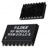
LC Series Transmitter Module
Data Guide
Description
0.360 in
The LC Series is ideally suited for volume use in
(9.14
mm) TXM-315-LC
OEM applications such as remote control, security,
LOT CTxxxx
identification and periodic data transfer. Housed
0.500 in
in a compact surface-mount package, the LC
(12.7 mm)
Series transmitter utilizes a highly-optimized SAW 0.150 in Max.
(3.81 mm)
architecture to achieve an unmatched blend of
performance, size, efficiency and cost. When
Figure 1: Package Dimensions
paired with a matching LR Series receiver, a
highly reliable wireless link is formed, capable of transferring serial data at
distances of up to 3,000 feet. No external RF components are required
(except an antenna), making design and integration straightforward, even
for engineers without previous RF experience.
Features
• Low cost
• No external RF components
required
• Ultra-low power consumption
• Compact surface-mount package
• Stable SAW-based architecture
• Supports data ranges to
5,000bps
• Wide supply range (2.7 to
5.2VDC)
• Direct serial interface
• Low harmonics
• No production tuning
Applications
•
•
•
•
•
•
Remote control
Keyless entry
Garage/gate openers
Lighting control
Medical monitoring/call systems
Remote industrial monitoring
•
•
•
•
•
•
– 1–
Periodic data transfer
Home/industrial automation
Fire/security alarms
Remote status/position sensing
Long-range RFID
Wire elimination
Revised 3/18/14
�Ordering Information
Electrical Specifications
Ordering Information
LC Series Transmitter Specifications
Part Number
Description
TXM-315-LC
315MHz Transmitter
TXM-418-LC
418MHz Transmitter
TXM-433-LC
433MHz Transmitter
EVAL-***-LC
LC Series Basic Evaluation Kit
Parameter
Symbol
Min.
Operating Voltage
VCC
2.7
Supply Current
lCC
Power Down Current
lPDN
Typ.
Max.
Units
Notes
5.2
VDC
6.0
mA
1,4
1.5
µA
2
Power Supply
*** = 315, 418 (Standard), 433MHz
Transmitters are supplied in tubes of 50 pcs.
3.0
Transmitter Section
Transmit Frequency
Figure 2: Ordering Information
Absolute Maximum Ratings
FC
TXM-315-LC
315
MHz
TXM-418-LC
418
MHz
TXM-433-LC
433.92
MHz
Center Frequency
Accuracy
Absolute Maximum Ratings
–75
Supply Voltage Vcc
−0.3
to
+6.0
VDC
Output Power
PO
Any Input or Output Pin
−0.3
to
VCC
VDC
Harmonic Emissions
PH
Operating Temperature
−30
to
+70
ºC
Data Rate
Storage Temperature
−45
to
+85
ºC
Data Input
Soldering Temperature
+260ºC for 10 seconds
Exceeding any of the limits of this section may lead to permanent damage to the device.
Furthermore, extended operation at these maximum ratings may reduce the life of this
device.
–4
0
+75
kHz
+4
dBm
3
–36
dBc
3
100
5,000
bps
Logic Low
VIL
0.0
0.4
VDC
Logic High
VIH
2.5
VCC
VDC
Antenna Port
RF Output Impedance
ROUT
Ω
5
80
µSec
5
100
nSec
5
+70
ºC
5
50
Timing
Figure 3: Absolute Maximum Ratings
Transmitter Turn-On Time
Warning: This product incorporates numerous static-sensitive
components. Always wear an ESD wrist strap and observe proper ESD
handling procedures when working with this device. Failure to observe
this precaution may result in module damage or failure.
30
Transmitter Turn-Off Time
Environmental
Operating Temperature
Range
1.
2.
Current draw with DATA pin held
continuously high
Current draw with DATA pin low
–30
3.
4.
5.
Figure 4: Electrical Specifications
– 2–
– 3–
RF out connected to a 50Ω load
LADJ through a 430Ω resistor
Characterized, but not tested
�Supply Current (mA)
Typical Performance Graphs
12
11
10
9
8
7
6
5
4
3
2
1
0
2.5
3.0
3.5
4.0
4.5
Supply Voltage (V)
5.0
With LADJ tied to ground
With 430Ω resistor on LADJ
Figure 7: Typical Oscillator Turn-On Time
Output Power (dBm)
Figure 5: Current vs. Supply Voltage
+8
+7
+6
+5
+4
+3
+2
+1
0
-1
-2
-3
-4
-5
2.5
3.0
3.5 4.0 4.5
Supply Voltage (V)
5.0
With LADJ tied to ground
With 430Ω resistor on LADJ
Figure 6: Output Power vs. Supply Voltage
– 4–
Figure 8: Oscillator Turn-Off Time
– 5–
�Output Power (dBm)
+8
+7
+6
+5
+4
+3
+2
+1
0
-1
-2
-3
-4
Pin Assignments
1
2
3
4
5V
3V
51 100 150 200 240 300 360 430 510 560 620 680 750 820 910 1.1K
LADJ Resistor Value (Ω)
Figure 9: Output Power vs. LADJ Resistor
GND
GND
DATA
VCC
GND
GND
LADJ/GND ANT
8
7
6
5
Figure 10: LC Series Transmitter Pinout (Top View)
Pin Descriptions
Pin Descriptions
Pin Number
Name
I/O
Description
1
GND
—
Analog Ground
2
DATA
I
3
GND
—
Digital Data Input
Analog Ground
Level Adjust. This line is used to adjust
the output power level of the transmitter.
Connecting to ground gives the highest
output, while pacing a resistor to ground
lowers the output level (see Figure 9 on
page 6)
4
LADJ/GND
I
5
ANT
—
50-ohm RF Output
6
GND
—
Analog Ground
7
VCC
—
Supply Voltage
8
GND
—
Analog Ground
Figure 11: Pin Descriptions
– 6–
– 7–
�Module Description
Theory of Operation
The LC Series transmitter is a low-cost, high-performance Surface
Acoustic Wave (SAW) based Carrier-Present Carrier-Absent (CPCA)
transmitter capable of sending serial data at up to 5,000bps. The LC’s
compact surface-mount package integrates easily into existing designs and
is equally friendly to prototype and volume production. Its ultra-low power
consumption makes it ideally suited for battery-powered products.
The LC Series transmitter transmits data using Carrier-Present CarrierAbsent (CPCA) modulation. This type of AM modulation is often referred to
by other designations, including Continuous
Wave (CW) and On-Off Key (OOK). This type
of modulation represents a logic low ‘0’ by Data
the absence of a carrier and a logic high ‘1’
Carrier
by the presence of a carrier. This method
affords numerous benefits. Three of the most
Figure 13: CPCA (AM) Modulation
important are:
The transmitter’s output power varies with supply voltage, but it is capable
of outputting +10dBm into a 50-ohm load. When combined with an LR
Series receiver, a reliable serial link is formed capable of transferring data
over line-of-site distances of up to 1.5 miles (2,500m) when used with
good antennas. Legal regulations in the various countries will require the
transmitter output power to be reduced which will reduce range. Following
the legal output limit for transmitters in the United States, systems based
on the LC Series transmitter and LR Series receiver can achieve ranges of
up to 3,000 feet (1,000m).
SAW
Oscillator
50Ω RF OUT
(ANT)
Data In
300-5,000bps
Keyed Output
Output Isolation
& Filter
Vcc
RF Amplifier
Figure 12: LC Series Transmitter Block Diagram
1) Cost-effectiveness due to design simplicity.
2) No minimum data rate or mark / space ratio requirement.
3) Higher output power and thus greater range in countries (such as the
U.S.) where output power measurements are averaged over time. (Please
refer to Linx Application Note AN-00130).
The LC Series transmitter is based on a simple but highly optimized
architecture that achieves a high fundamental output power with low
harmonic content. This ensures that approval requirements can be
met without external filter components. The LC Series transmitter is
exceptionally stable over time, temperature, and physical shock as a result
of the precision Surface Acoustic Wave (SAW) frequency reference. Due to
the accuracy of the SAW device, most of the output power is concentrated
in a narrow bandwidth. This allows the receiver’s bandwidth to be quite
narrow, thus increasing sensitivity and reducing susceptibility to near-band
interference. The quality of components and overall architecture utilized in
the module is extraordinary in a low-cost RF device and is one reason why
the LC Series transmitter is able to outperform more expensive products.
The Data Input
A CMOS / TTL level data input is provided on Pin 2. This line is normally
supplied with a serial bit stream input directly from a microprocessor,
encoder or UART. During standby, or the input of a logic low, the carrier is
fully suppressed and the transmitter consumes less than 2μA of current.
During a logic high, the transmitter generates a carrier to indicate to the
receiver the presence of a logic ‘1’. The applied data should not exceed a
rate of 5,000bps. The data input line should always be driven with a voltage
common to the supply voltage present on Pin 7 (VCC) and should never be
allowed to exceed the supply voltage.
– 8–
– 9–
�Adjusting the Output Power
Transferring Data
Depending on the type of antenna being used and the duty cycle of the
data, the output power of the LC Series transmitter module may be higher
than FCC regulations allow. The output power of the module is intentionally
set high to compensate for losses resulting from inefficient antennas that
may be used to realize cost or space savings. Since attenuation is often
required, it is generally wise to provide for its implementation and allow the
FCC test lab to easily attenuate the transmitter to the maximum legal limit
for your product.
Once a reliable RF link has been established, the challenge becomes how
to effectively transfer data across it. While a properly designed RF link
provides reliable data transfer under most conditions, there are still distinct
differences from a wired link that must be addressed. The LC Series is
intended to be as transparent as possible and does not incorporate internal
encoding or decoding, so a user has tremendous flexibility in how data is
handled.
Two methods of attenuation are available using the LC Series transmitter
module. First, a resistor may be placed between Pin 4 (LADJ) and
ground to achieve up to a 7dB reduction in output power. The resistor
value is easily determined from Figure 9 on page 6. Do not exceed
the resistance values shown as transmitter instability may result. This
method can also be used to reduce the transmission range and power
consumption.
Another method commonly used to achieve attenuation, particularly at
higher levels, is the use of a T-pad attenuator. A T-pad is a network of three
resistors that allows for variable attenuation while maintaining the correct
match to the antenna. It is usually prudent to allow space for the addition
of a T-pad. An example of a T-pad attenuator layout is shown in Figure 14.
For further details on T-pad attenuators, please refer to Application Note
AN-00150.
TYPICAL LAYOUT
CIRCUIT
WITH PROVISION FOR ATTENUATION
ANT
PADS FOR SMD
RESISTORS
R1
R1
ANT
R2
GROUND PLANE
ON LOWER LAYER
GROUND
GND
ANT OUT
TXM-xxx-LC
LOT CTxxxx
If the product transfers simple control or status signals such as button
presses or switch closures and it does not have a microprocessor on board
(or it is desired to avoid protocol development), consider using a remote
control encoder and decoder or a transcoder IC. These chips are available
from a wide range of manufacturers including Linx. They take care of all
encoding and decoding functions, and generally provide a number of data
pins to which switches can be directly connected. In addition, address bits
are usually provided for security and to allow the addressing of multiple
units independently. These ICs are an excellent way to bring basic remote
control / status products to market quickly and inexpensively. Additionally,
it is a simple task to interface with inexpensive microprocessors, IR, remote
control or modem ICs.
It is always important to separate the types of transmissions that are
technically possible from those that are legally allowable in the country
of intended operation. Linx Application Notes AN-00125, AN-00128
and AN-00140 should be reviewed, along with Part 15, Section 231 of
the Code of Federal Regulations for further details regarding acceptable
transmission content in the US All of these documents can be downloaded
from the Linx website at www.linxtechnologies.com.
Another area of consideration is that the data structure can affect the
output power level. The FCC allows output power in the 260 to 470MHz
band to be averaged over a 100ms time frame. Because OOK modulation
activates the carrier for a ‘1’ and deactivates the carrier for a ‘0’, a data
stream that sends more ‘0’s has a lower average output power over
100ms. This allows the instantaneous output power to be increased, thus
extending range.
Figure 14: A T-Pad Attenuator Layout Example
– 10 –
– 11 –
�Power Supply Requirements
The module does not have an internal
Vcc TO
MODULE
voltage regulator; therefore it requires a
clean, well-regulated power source. While
10Ω
it is preferable to power the unit from a
Vcc IN
battery, the unit can also be operated from
10µF
a power supply as long as noise is less than
20mV. Power supply noise can significantly
affect the transmitter modulation; therefore,
providing a clean power supply for the
Figure 15: Supply Filter
module should be a high design priority.
+
A 10-ohm resistor in series with the supply followed by a 10μF tantalum
capacitor from VCC to ground will help in cases where the quality of supply
power is poor. These values may need to be adjusted depending on the
noise present on the supply line.
Typical Applications
The LC Series transmitter is ideal for the transmission of remote control /
command data. One of the easiest way to transmit on / off data or switch
closures is to use an encoder and decoder. These ICs provide a number
of data lines that can be connected to switches or buttons or even a
microcontroller. When a line is taken high on the encoder, a corresponding
line goes high on the decoder as long as the address matches. Figure 16
shows an example using the Linx MS Series encoder.
750
1
GND
GND
2
DATA
VCC
3
GND
GND
4
LADJ/GND ANT
8
7
6
5
TXM-xxx-LC
100k
100k
220
1
2
3
4
5
6
7
8
9
10
0
The MS Series Encoder Data Guide explains this circuit and the many
features of the encoder in detail, so please refer to that document for more
information.
A 750-ohm resistor is used on the LADJ line of the transmitter to reduce
the output power of the transmitter. This is appropriate for some antennas,
but may need to be adjusted depending on the design. Typically, a
resistor pad is placed on the board and a potentiometer is used by the
FCC test lab to adjust the output power to the maximum legal limit. The
potentiometer value is measured and the closest standard value resistor is
placed for final testing.
If the level adjust resistor does not provide enough attenuation, a T-pad
attenuator can be placed between the transmitter and antenna. This is a
network of three resistors that provides a set amount of attenuation while
maintaining a 50-ohm match between the antenna and the transmitter.
Application Note AN-00150 gives the formulas for calculating the resistor
values. If not needed, the series resistors can be zero ohms or shorted and
the parallel one not placed.
ESD Concerns
0
OPEN
D6
D5
D7
D4
SEL_BAUD0
D3
SEL_BAUD1
D2
GND
VCC
GND
VCC
GND
D1
TX_CNTL
D0
DATA_OUT
SEND
MODE_IND CREATE_ADDR
This circuit uses the LC Series transmitter and the MS Series encoder to
transmit button presses. The MS Series has eight data lines, which are
connected to buttons that pull the line high when pressed. When not used,
the lines are pulled low by 100k-ohm resistors. The encoder begins a
transmission when the SEND line is taken high. Diodes are used to pull this
line high when any data line is pulled high while isolating the data lines from
each other.
20
19
18
17
16
15
14
13
12
11
100k
100k
100k
100k
The module has basic ESD protection built in, but in cases where the
antenna connection is exposed to the user it is a good idea to add
additional protection. A Transient Voltage Suppressor (TVS) diode, varistor
or similar component can be added to the antenna line. These should have
low capacitance and be designed for use on antennas. Protection on the
supply line is a good idea in designs that have a user-accessible power
port.
100k
100k
220
100k
LICAL-ENC-MS001
Figure 16: LC Series Transmitter and MS Series Encoder
– 12 –
– 13 –
�Antenna Considerations
Helpful Application Notes from Linx
The choice of antennas is a
critical and often overlooked
design consideration. The range,
performance and legality of an RF
link are critically dependent upon the
antenna. While adequate antenna
performance can often be obtained
by trial and error methods, antenna
Figure 17: Linx Antennas
design and matching is a complex
task. Professionally designed antennas such as those from Linx (Figure
17) help ensure maximum performance and FCC and other regulatory
compliance.
It is not the intention of this manual to address in depth many of the issues
that should be considered to ensure that the modules function correctly
and deliver the maximum possible performance. We recommend reading
the application notes listed in Figure 18 which address in depth key areas
of RF design and application of Linx products. These applications notes are
available online at www.linxtechnologies.com or by contacting Linx.
Linx transmitter modules typically have an output power that is higher
than the legal limits. This allows the designer to use an inefficient antenna
such as a loop trace or helical to meet size, cost or cosmetic requirements
and still achieve full legal output power for maximum range. If an efficient
antenna is used, then some attenuation of the output power will likely be
needed. This can easily be accomplished by using the LADJ line.
A receiver antenna should be optimized for the frequency or band in
which the receiver operates and to minimize the reception of off-frequency
signals. The efficiency of the receiver’s antenna is critical to maximizing
range performance. Unlike the transmitter antenna, where legal operation
may mandate attenuation or a reduction in antenna efficiency, the receiver’s
antenna should be optimized as much as is practical.
It is usually best to utilize a basic quarter-wave whip until your prototype
product is operating satisfactorily. Other antennas can then be evaluated
based on the cost, size and cosmetic requirements of the product.
Additional details are in Application Note AN-00500.
Helpful Application Note Titles
Note Number
Note Title
AN-00100
RF 101: Information for the RF Challenged
AN-00125
Considerations for Operation Within the 260–470MHz Band
AN-00130
Modulation Techniques for Low-Cost RF Data Links
AN-00140
The FCC Road: Part 15 from Concept to Approval
AN-00150
Use and Design of T-Attenuation Pads
AN-00160
Considerations for Sending Data over a Wireless Link
AN-00232
General Considerations for Sending Data with the LC Series
AN-00500
Antennas: Design, Application, Performance
AN-00501
Understanding Antenna Specifications and Operation
Figure 18: Helpful Application Note Titles
Protocol Guidelines
While many RF solutions impose data formatting and balancing
requirements, Linx RF modules do not encode or packetize the signal
content in any manner. The received signal will be affected by such factors
as noise, edge jitter and interference, but it is not purposefully manipulated
or altered by the modules. This gives the designer tremendous flexibility for
protocol design and interface.
Despite this transparency and ease of use, it must be recognized that there
are distinct differences between a wired and a wireless environment. Issues
such as interference and contention must be understood and allowed for in
the design process. To learn more about protocol considerations, read Linx
Application Note AN-00160.
Interference or changing signal conditions can corrupt the data packet,
so it is generally wise to structure the data being sent into small packets.
This allows errors to be managed without affecting large amounts of data.
A simple checksum or CRC could be used for basic error detection. Once
an error is detected, the protocol designer may wish to simply discard the
corrupt data or implement a more sophisticated scheme to correct it.
– 14 –
– 15 –
�Interference Considerations
Pad Layout
The RF spectrum is crowded and the potential for conflict with unwanted
sources of RF is very real. While all RF products are at risk from
interference, its effects can be minimized by better understanding its
characteristics.
The pad layout diagram in Figure 19 is designed to facilitate both hand and
automated assembly.
Interference may come from internal or external sources. The first step
is to eliminate interference from noise sources on the board. This means
paying careful attention to layout, grounding, filtering and bypassing in
order to eliminate all radiated and conducted interference paths. For
many products, this is straightforward; however, products containing
components such as switching power supplies, motors, crystals and other
potential sources of noise must be approached with care. Comparing your
own design with a Linx evaluation board can help to determine if and at
what level design-specific interference is present.
External interference can manifest itself in a variety of ways. Low-level
interference produces noise and hashing on the output and reduces the
link’s overall range.
High-level interference is caused by nearby products sharing the same
frequency or from near-band high-power devices. It can even come from
your own products if more than one transmitter is active in the same area.
It is important to remember that only one transmitter at a time can occupy
a frequency, regardless of the coding of the transmitted signal. This type of
interference is less common than those mentioned previously, but in severe
cases it can prevent all useful function of the affected device.
Although technically not interference, multipath is also a factor to be
understood. Multipath is a term used to refer to the signal cancellation
effects that occur when RF waves arrive at the receiver in different phase
relationships. This effect is a particularly significant factor in interior
environments where objects provide many different signal reflection paths.
Multipath cancellation results in lowered signal levels at the receiver and
shorter useful distances for the link.
0.065"
0.340"
0.070"
0.100"
Figure 19: Recommended PCB Layout
Board Layout Guidelines
The module’s design makes integration straightforward; however, it
is still critical to exercise care in PCB layout. Failure to observe good
layout techniques can result in a significant degradation of the module’s
performance. A primary layout goal is to maintain a characteristic
50-ohm impedance throughout the path from the antenna to the module.
Grounding, filtering, decoupling, routing and PCB stack-up are also
important considerations for any RF design. The following section provides
some basic design guidelines.
During prototyping, the module should be soldered to a properly laid-out
circuit board. The use of prototyping or “perf” boards results in poor
performance and is strongly discouraged. Likewise, the use of sockets
can have a negative impact on the performance of the module and is
discouraged.
The module should, as much as reasonably possible, be isolated from
other components on your PCB, especially high-frequency circuitry such as
crystal oscillators, switching power supplies, and high-speed bus lines.
When possible, separate RF and digital circuits into different PCB regions.
– 16 –
– 17 –
�Make sure internal wiring is routed away from the module and antenna and
is secured to prevent displacement.
Do not route PCB traces directly under the module. There should not be
any copper or traces under the module on the same layer as the module,
just bare PCB. The underside of the module has traces and vias that could
short or couple to traces on the product’s circuit board.
The Pad Layout section shows a typical PCB footprint for the module. A
ground plane (as large and uninterrupted as possible) should be placed on
a lower layer of your PC board opposite the module. This plane is essential
for creating a low impedance return for ground and consistent stripline
performance.
Use care in routing the RF trace between the module and the antenna
or connector. Keep the trace as short as possible. Do not pass it under
the module or any other component. Do not route the antenna trace on
multiple PCB layers as vias add inductance. Vias are acceptable for tying
together ground layers and component grounds and should be used in
multiples.
Microstrip Details
A transmission line is a medium whereby RF energy is transferred from
one place to another with minimal loss. This is a critical factor, especially
in high-frequency products like Linx RF modules, because the trace
leading to the module’s antenna can effectively contribute to the length
of the antenna, changing its resonant bandwidth. In order to minimize
loss and detuning, some form of transmission line between the antenna
and the module should be used unless the antenna can be placed very
close (