DA14581
Bluetooth Low Energy 4.2 SoC with Optimized Boot Time
General Description
FINAL
AES-128 bit encryption Processor
Memories
The DA14581 integrated circuit is an optimized version
32 kB One-Time-Programmable (OTP) memory
of the DA14580, offering a reduced boot time and sup 42 kB System SRAM
porting up to 8 connections. It has a fully integrated
84 kB ROM
radio transceiver and baseband processor for Blue 8 kB Retention SRAM
®
tooth low energy. It can be used as a standalone
Power management
application processor or as a data pump in hosted sys Integrated Buck/Boost DC-DC converter
tems.
P0, P1 and P2 ports with 3.3 V tolerance
Easy decoupling of only 4 supply pins
The DA14581 supports a flexible memory architecture
Supports coin (typ. 3.0 V) and alkaline (typ. 1.5 V)
for storing Bluetooth profiles and custom application
battery cells
code, which can be updated over the air (OTA). The
10-bit ADC for battery voltage measurement
qualified Bluetooth low energy protocol stack and the
Digital controlled oscillators
HCI ready software are stored in a dedicated ROM. All
16 MHz crystal (±20 ppm max) and RC oscillator
software runs on the ARM® Cortex®-M0 processor via
32 kHz crystal (±50 ppm, ±500 ppm max) and
a simple scheduler.
RCX oscillator
The Bluetooth low energy firmware includes the
General purpose, Capture and Sleep timers
L2CAP service layer protocols, Security Manager
Digital interfaces
(SM), Attribute Protocol (ATT), the Generic Attribute
Gen. purpose I/Os: 14 (WLCSP34), 24 (QFN40)
Profile (GATT) and the Generic Access Profile (GAP).
2 UARTs with hardware flow control up to 1 MBd
All profiles published by the Bluetooth SIG as well as
SPI+™ interface
custom profiles are supported.
I2C bus at 100 kHz, 400 kHz
3-axes capable Quadrature Decoder
The transceiver interfaces directly to the antenna and
Analog interfaces
is fully compliant with the Bluetooth 4.2 standard.
4-channel 10-bit ADC
The DA14581 has dedicated hardware for the Link
Radio transceiver
Layer implementation of Bluetooth low energy and
Fully integrated 2.4 GHz CMOS transceiver
interface controllers for enhanced connectivity capabili Single wire antenna: no RF matching or RX/TX
ties.
switching required
Supply current at VBAT3V:
Features
TX: 3.4 mA, RX: 3.7 mA (with ideal DC-DC)
Complies with Bluetooth V4.2, ETSI EN 300 328 and
0 dBm transmit output power
-20 dBm output power in “Near Field Mode”
EN 300 440 Class 2 (Europe), FCC CFR47 Part 15
-93 dBm receiver sensitivity
(US) and ARIB STD-T66 (Japan)
Supports up to 8 Bluetooth low energy connections
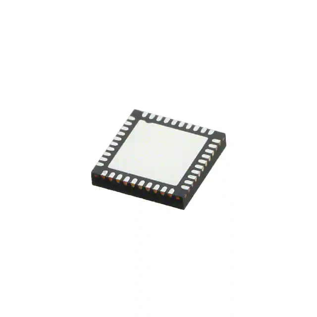
Packages:
Fast cold boot in less than 30 ms
Ultra-Thin WLCSP 34 pins, 2.436 mm x 2.436 mm
Processing power
x 0.334 mm
16 MHz 32 bit ARM Cortex-M0 with SWD inter WLCSP 34 pins, 2.436 mm x 2.436 mm
face
x 0.511 mm
Dedicated Link Layer Processor
QFN 40 pins, 5 mm x 5 mm
________________________________________________________________________________________________
A
C
O
N
FI
D
EN
TI
AL
N
D
System Diagram
Datasheet
CFR0011-120-01
Revision 3.3
1 of 233
30-Dec-2021
© 2021 Renesas Electronics
�DA14581
Bluetooth Low Energy 4.2 SoC with Optimized Boot Time
FINAL
Contents
General Description . . . . . . . . . . . . . . . . . . . . . . . . . . . 1
11.4 GENERAL CLOCK CONSTRAINTS . . . . . . . 31
Features . . . . . . . . . . . . . . . . . . . . . . . . . . . . . . . . . . . . . 1
12 OTP Controller. . . . . . . . . . . . . . . . . . . . . . . . . . . . 32
System Diagram . . . . . . . . . . . . . . . . . . . . . . . . . . . . . . 1
12.1 OPERATING MODES . . . . . . . . . . . . . . . . . . 32
12.2 AHB MASTER INTERFACE . . . . . . . . . . . . . 32
Contents. . . . . . . . . . . . . . . . . . . . . . . . . . . . . . . . . . . . . 2
13 I2C Interface. . . . . . . . . . . . . . . . . . . . . . . . . . . . . . 33
1 Block Diagram . . . . . . . . . . . . . . . . . . . . . . . . . . . . . . 4
13.1 I2C BUS TERMS . . . . . . . . . . . . . . . . . . . . . . 33
2 Pinout . . . . . . . . . . . . . . . . . . . . . . . . . . . . . . . . . . . . . 5
TI
AL
13.1.1 Bus Transfer Terms . . . . . . . . . . . . . . . 34
13.2 I2C BEHAVIOR . . . . . . . . . . . . . . . . . . . . . . . 34
3 Ordering Information . . . . . . . . . . . . . . . . . . . . . . . . 8
13.2.1 START and STOP Generation . . . . . . . 35
13.2.2 Combined Formats . . . . . . . . . . . . . . . 35
4.1 INTERNAL BLOCKS . . . . . . . . . . . . . . . . . . . . . 9
13.3 I2C PROTOCOLS . . . . . . . . . . . . . . . . . . . . . 35
4.2 FUNCTIONAL MODES . . . . . . . . . . . . . . . . . . . 9
13.3.1 START and STOP Conditions . . . . . . . 35
4.3 OTP MEMORY LAYOUT . . . . . . . . . . . . . . . . 10
13.3.2 Addressing Slave Protocol. . . . . . . . . . 35
4.3.1 OTP Header. . . . . . . . . . . . . . . . . . . . . . 10
4.4 SYSTEM START PROCEDURE . . . . . . . . . . . .11
4.4.1 Power/Wake-Up Sequence . . . . . . . . . . 12
13.3.3 Transmitting and Receiving Protocols . 36
13.4 MULTIPLE MASTER ARBITRATION . . . . . . 38
13.5 CLOCK SYNCHRONIZATION . . . . . . . . . . . 39
13.6 OPERATION MODES . . . . . . . . . . . . . . . . . . 40
FI
D
4.4.2 OTP Mirroring . . . . . . . . . . . . . . . . . . . . 13
EN
4 System Overview. . . . . . . . . . . . . . . . . . . . . . . . . . . . 9
4.4.3 BootROM Sequence . . . . . . . . . . . . . . . 14
13.6.1 Slave Mode Operation . . . . . . . . . . . . . 40
4.5 POWER SUPPLY CONFIGURATION . . . . . . 16
13.6.2 Master Mode Operation . . . . . . . . . . . . 42
4.5.1 Power Domains . . . . . . . . . . . . . . . . . . . 16
13.6.3 Disabling the I2C Controller . . . . . . . . . 42
4.5.2 Power Modes . . . . . . . . . . . . . . . . . . . . . 17
14 UART . . . . . . . . . . . . . . . . . . . . . . . . . . . . . . . . . . . 43
14.1 UART (RS232) SERIAL PROTOCOL . . . . . . 44
N
4.5.3 Retention Registers . . . . . . . . . . . . . . . . 17
14.2 IRDA 1.0 SIR PROTOCOL . . . . . . . . . . . . . . 44
5.1 POR, HW AND SW RESET . . . . . . . . . . . . . . 19
14.3 CLOCK SUPPORT . . . . . . . . . . . . . . . . . . . . 45
O
5 Reset. . . . . . . . . . . . . . . . . . . . . . . . . . . . . . . . . . . . . 19
14.4 INTERRUPTS . . . . . . . . . . . . . . . . . . . . . . . . 46
6 ARM Cortex-M0 . . . . . . . . . . . . . . . . . . . . . . . . . . . . 20
14.5 PROGRAMMABLE THRE INTERRUPT . . . . 46
C
6.1 INTERRUPTS . . . . . . . . . . . . . . . . . . . . . . . . . 21
14.6 SHADOW REGISTERS . . . . . . . . . . . . . . . . 48
6.2 SYSTEM TIMER (SYSTICK). . . . . . . . . . . . . . 22
14.7 DIRECT TEST MODE . . . . . . . . . . . . . . . . . . 48
6.3 WAKE-UP INTERRUPT CONTROLLER. . . . . 22
A
6.4 REFERENCE . . . . . . . . . . . . . . . . . . . . . . . . . 22
15 SPI+ Interface . . . . . . . . . . . . . . . . . . . . . . . . . . . . 49
15.1 OPERATION WITHOUT FIFOS . . . . . . . . . . 49
D
7 AMBA Bus Overview. . . . . . . . . . . . . . . . . . . . . . . . 23
N
8 Patch Block . . . . . . . . . . . . . . . . . . . . . . . . . . . . . . . 24
9 Memory Map . . . . . . . . . . . . . . . . . . . . . . . . . . . . . . 25
10 Memory Controller . . . . . . . . . . . . . . . . . . . . . . . . 27
10.1 ARBITRATION . . . . . . . . . . . . . . . . . . . . . . . 27
15.2 9 BITS MODE . . . . . . . . . . . . . . . . . . . . . . . . 50
16 Quadrature Decoder . . . . . . . . . . . . . . . . . . . . . . . 53
17 Wake-Up Timer . . . . . . . . . . . . . . . . . . . . . . . . . . . 54
18 General Purpose Timers. . . . . . . . . . . . . . . . . . . . 55
18.1 TIMER 0 . . . . . . . . . . . . . . . . . . . . . . . . . . . . 55
11 Clock Generation. . . . . . . . . . . . . . . . . . . . . . . . . . 28
11.1 CRYSTAL OSCILLATORS . . . . . . . . . . . . . . 28
11.1.1 FRequency Control (16 MHz Crystal) . 28
18.2 TIMER 2 . . . . . . . . . . . . . . . . . . . . . . . . . . . . 57
19 Watchdog Timer . . . . . . . . . . . . . . . . . . . . . . . . . . 59
11.1.2 Automated Trimming Mechanism . . . . 28
20 Keyboard Controller . . . . . . . . . . . . . . . . . . . . . . . 60
11.2 RC OSCILLATORS . . . . . . . . . . . . . . . . . . . . 29
20.1 KEYBOARD SCANNER . . . . . . . . . . . . . . . . 60
11.2.1 Frequency Calibration . . . . . . . . . . . . . 29
20.2 GPIO INTERRUPT GENERATOR . . . . . . . . 60
11.3 SYSTEM CLOCK GENERATION . . . . . . . . . 30
Datasheet
CFR0011-120-01
Revision 3.3
2 of 233
30-Dec-2021
© 2021 Renesas Electronics
�DA14581
Bluetooth Low Energy 4.2 SoC with Optimized Boot Time
FINAL
21 Input/Output Ports. . . . . . . . . . . . . . . . . . . . . . . . . 62
21.1 PROGRAMMABLE PIN ASSIGNMENT . . . . 62
21.2 GENERAL PURPOSE PORT REGISTERS . 62
21.2.1 Port Data Register . . . . . . . . . . . . . . . . 63
21.2.2 Port Set Data Output Register . . . . . . . 63
21.2.3 Port Reset Data Output Register . . . . . 63
21.3 FIXED ASSIGNMENT FUNCTIONALITY . . . 63
TI
AL
22 General Purpose ADC. . . . . . . . . . . . . . . . . . . . . . 64
22.1 INPUT CHANNELS AND INPUT SCALE . . . 64
22.2 STARTING THE ADC AND SAMPLING RATE
. . . . . . . . . . . . . . . . . . . . . . . . . . . . . . . . . . . 64
22.3 NON-IDEAL EFFECTS . . . . . . . . . . . . . . . . . 65
22.4 CHOPPING . . . . . . . . . . . . . . . . . . . . . . . . . . 65
22.6 ZERO-SCALE ADJUSTMENT . . . . . . . . . . . 66
22.7 COMMON MODE ADJUSTMENT. . . . . . . . . 66
22.8 INPUT IMPEDANCE, INDUCTANCE AND INPUT SETTLING. . . . . . . . . . . . . . . . . . . . . . . . 66
FI
D
22.9 DELAY COUNTER . . . . . . . . . . . . . . . . . . . . 67
EN
22.5 OFFSET CALIBRATION . . . . . . . . . . . . . . . . 65
23 Power Management. . . . . . . . . . . . . . . . . . . . . . . . 68
24 BLE Core . . . . . . . . . . . . . . . . . . . . . . . . . . . . . . . . 71
24.1 EXCHANGE MEMORY . . . . . . . . . . . . . . . . . 71
N
24.2 PROGRAMMING BLE WAKE UP IRQ . . . . . 73
24.3 SWITCH FROM ACTIVE MODE TO DEEP
O
SLEEP MODE . . . . . . . . . . . . . . . . . . . . . . . . . 73
24.4 SWITCH FROM DEEP SLEEP MODE TO AC-
C
TIVE MODE. . . . . . . . . . . . . . . . . . . . . . . . . . . 74
24.4.1 Switching at Anchor Points . . . . . . . . . 74
24.4.2 Switching Due to an External Event . . 76
A
25 Radio . . . . . . . . . . . . . . . . . . . . . . . . . . . . . . . . . . . 77
25.1 RECEIVER . . . . . . . . . . . . . . . . . . . . . . . . . . 77
D
25.2 SYNTHESIZER . . . . . . . . . . . . . . . . . . . . . . . 77
25.3 TRANSMITTER . . . . . . . . . . . . . . . . . . . . . . . 77
N
25.4 RFIO . . . . . . . . . . . . . . . . . . . . . . . . . . . . . . . 77
25.5 BIASING . . . . . . . . . . . . . . . . . . . . . . . . . . . . 77
25.6 CONTROL . . . . . . . . . . . . . . . . . . . . . . . . . . . 77
26 Registers . . . . . . . . . . . . . . . . . . . . . . . . . . . . . . . . 78
27 Specifications . . . . . . . . . . . . . . . . . . . . . . . . . . . 217
28 Package Information . . . . . . . . . . . . . . . . . . . . . . 229
28.1 MOISTURE SENSITIVITY LEVEL (MSL) . . 229
28.2 WLCSP HANDLING . . . . . . . . . . . . . . . . . . 229
28.3 SOLDERING INFORMATION . . . . . . . . . . . 229
28.4 PACKAGE OUTLINES . . . . . . . . . . . . . . . . 230
Datasheet
CFR0011-120-01
Revision 3.3
3 of 233
30-Dec-2021
© 2021 Renesas Electronics
�DA14581
Bluetooth Low Energy 4.2 SoC with Optimized Boot Time
24 April 2012
ARM Cortex M0
XTAL
32.768 kHz
XTAL
16 MHz
CORE
BLE Core
LDO
RET
RC
16 MHz
LDO
LDO
LDO
SYS
SYS
RF
RCX
Radio
Transceiver
N
Timer 2
3xPWM
QUAD
DECODER
GP ADC
I2C
FIFO
SPI
UART2
FIFO
Timer 0
1xPWM
UART
SW TIMER
FIFO
C
O
APB bridge
RC
32 kHz
POReset
LINK LAYER
HARDWARE
KEYBOARD
CTRL
OTPC
N
ROM
84 kB
DMA
POWER/CLOCK
Management (PMU)
OTP
32 kB
A
Ret. RAM4
1 kB
D
Ret. RAM3
2 kB
Memory Controller
Ret. RAM2
3 kB
LDO
SYS
AES-128
System/
Exchange
RAM
42 kB
Ret. RAM
2 kB
DCDC
(BUCK/BOOST)
FI
D
SWD (JTAG)
EN
TI
AL
Block Diagram
WAKE UP
TIMER
1
FINAL
GPIO MULTIPLEXING
Figure 1: DA14581 Block Diagram
Datasheet
CFR0011-120-01
Revision 3.3
4 of 233
30-Dec-2021
© 2021 Renesas Electronics
�DA14581
Bluetooth Low Energy 4.2 SoC with Optimized Boot Time
Pinout
• A Quad Flat Package No Leads (QFN) with 40 pins
The actual pin/ball assignment is depicted in the following figures:
TI
AL
VP
P
G
N
G
5
P0
_
XT
AL
32
Kp
XT
AL
32
Km
D
VB
AT
3V
EN
P0
_6
P0
_4
P0
_
VB
AT
_R
F
P0
_7
N
G
ST
R
P0
_
2
P0
_1
N
G
G
N
D
D
P1
_
P1
_1
C
D
VD
C
6
N
D
5
D
R
FI
O
m
4
G
N
D
2
LK
_C
SW
SW
F
IT
C
H
E
3
P1
_0
D
D
IO
C
SW
B
VB
AT
1V
A
2
XT
XT
AL
AL
16
16
M
M
m
p
VD
C
P1
D
C
_3
_R
F
1
P0
_0
• A Wafer Level Chip Scale Package (WLCSP) with
34 balls (normal thickness and ultra-thin)
3
The DA14581 comes in three packages:
R
FI
O
p
2
FINAL
FI
D
DA14581 (Top View)
VPP
P2_8
P2_7
RFIOp
RFIOm
P2_6
P2_5
VDCDC_RF
37
36
35
34
33
32
31
P2_9
P0_0
1
30
P0_1
2
29
XTAL16Mp
P0_2
3
28
P1_3
P0_3
4
NC
5
P0_4
6
P0_5
7
P2_1
C
XTAL16Mm
19
20
VDCDC
P2_4
Pin 0: GND
plane
18
SWITCH
P2_3
21
17
10
RST
P1_0
P0_7
16
P0_6
GND
VBAT1V
22
15
23
9
VBAT3V
8
14
P1_1
VBAT_RF
SWDIO
24
13
25
12
(Top View)
P2_2
SW_CLK
XTAL32Kp
P1_2
26
11
27
DA14581
XTAL32Km
A
D
N
39
40
O
P2_0
N
38
Figure 2: WLCSP Ball Assignment
Figure 3: QFN40 Pin Assignment
Datasheet
CFR0011-120-01
Revision 3.3
5 of 233
30-Dec-2021
© 2021 Renesas Electronics
�DA14581
Bluetooth Low Energy 4.2 SoC with Optimized Boot Time
FINAL
Table 1: Pin Description
Pin Name
Type
Drive
(mA)
Reset
State
Description
General Purpose I/Os
DIO
DIO
DIO
DIO
DIO
DIO
DIO
DIO
4.8
I-PD
I-PD
I-PD
I-PD
I-PD
I-PD
I-PD
I-PD
INPUT/OUTPUT with selectable pull up/down resistor. Pull-down
enabled during and after reset. General purpose I/O port bit or
alternate function nodes. Contains state retention mechanism
during power down.
P1_0
P1_1
P1_2
P1_3
P1_4/SWCLK
P1_5/SW_DIO
DIO
DIO
DIO
DIO
DIO
DIO
4.8
I-PD
I-PD
I-PD
I-PD
I-PD
I-PU
INPUT/OUTPUT with selectable pull up/down resistor. Pull-down
enabled during and after reset. General purpose I/O port bit or
alternate function nodes. Contains state retention mechanism
during power down.
This signal is the JTAG clock by default
This signal is the JTAG data I/O by default
P2_0
P2_1
P2_2
P2_3
P2_4
P2_5
P2_6
P2_7
P2_8
P2_9
DIO
DIO
DIO
DIO
DIO
DIO
DIO
DIO
DIO
DIO
4.8
I-PD
I-PD
I-PD
I-PD
I-PD
I-PD
I-PD
I-PD
I-PD
I-PD
INPUT/OUTPUT with selectable pull up/down resistor. Pull-down
enabled during and after reset. General purpose I/O port bit or
alternate function nodes. Contains state retention mechanism
during power down.
NOTE: This port is only available on the QFN40 package.
P3_0 to P3_7
DIO
4.8
I-PD
Not supported.
DIO
SW_CLK/
P1_4
DIO
Clocks
EN
FI
D
N
4.8
C
SWDIO/P1_5
O
Debug interface
TI
AL
P0_0
P0_1
P0_2
P0_3
P0_4
P0_5
P0_6
P0_7
4.8
I-PU
INPUT/OUTPUT. JTAG Data input/output. Bidirectional data and
control communication. Can also be used as a GPIO
I-PD
INPUT JTAG clock signal. Can also be used as a GPIO
AI
INPUT. Crystal input for the 16 MHz XTAL
XTAL16Mm
AO
OUTPUT. Crystal output for the 16 MHz XTAL
XTAL32kp
AI
INPUT. Crystal input for the 32.768 kHz XTAL
AO
OUTPUT. Crystal output for the 32.768 kHz XTAL
D
A
XTAL16Mp
XTAL32km
N
Quadrature Decoder
QD_CHA_X
DI
INPUT. Channel A for the X axis. Mapped on Px ports
QD_CHB_X
DI
INPUT. Channel B for the X axis. Mapped on Px ports
QD_CHA_Y
DI
INPUT. Channel A for the Y axis. Mapped on Px ports
QD_CHB_Y
DI
INPUT. Channel B for the Y axis. Mapped on Px ports
QD_CHA_Z
DI
INPUT. Channel A for the Z axis. Mapped on Px ports
QD_CHB_Z
DI
INPUT. Channel B for the Z axis. Mapped on Px ports
DO
INPUT/OUTPUT. SPI Clock. Mapped on Px ports
SPI_DI
DI
INPUT. SPI Data input. Mapped on Px ports
SPI_DO
DO
OUTPUT. SPI Data output. Mapped on Px ports
SPI Bus Interface
SPI_CLK
Datasheet
CFR0011-120-01
Revision 3.3
6 of 233
30-Dec-2021
© 2021 Renesas Electronics
�DA14581
Bluetooth Low Energy 4.2 SoC with Optimized Boot Time
FINAL
Table 1: Pin Description
Pin Name
Drive
(mA)
Type
SPI_EN
Reset
State
DI
Description
INPUT. SPI Clock enable. Mapped on Px ports
I2C Bus Interface
DIO/DIOD
INPUT/OUTPUT. I2C bus Data with open drain port. Mapped on
Px ports
SCL
DIO/DIOD
INPUT/OUTPUT. I2C bus Clock with open drain port. In open
drain mode, SCL is monitored to support bit stretching by a
slave. Mapped on Px ports.
TI
AL
SDA
UART Interface
UTX
DO
OUTPUT. UART transmit data. Mapped on Px ports
URX
DI
INPUT. UART receive data. Mapped on Px ports
URTS
DO
OUTPUT. UART Request to Send. Mapped on Px ports
UCTS
DI
INPUT. UART Clear to Send. Mapped on Px ports
DO
OUTPUT. UART 2 transmit data. Mapped on Px ports
DI
INPUT. UART 2 receive data. Mapped on Px ports
URTS2
DO
OUTPUT. UART 2 Request to Send. Mapped on Px ports
UCTS2
DI
INPUT. UART 2 Clear to Send. Mapped on Px ports
EN
UTX2
URX2
AI
ADC[1]
AI
ADC[2]
AI
ADC[3]
AI
INPUT. Analog to Digital Converter input 0. Mapped on P0[0]
INPUT. Analog to Digital Converter input 1. Mapped on P0[1]
INPUT. Analog to Digital Converter input 2. Mapped on P0[2]
INPUT. Analog to Digital Converter input 3. Mapped on P0[3]
N
ADC[0]
FI
D
Analog Interface
Radio Transceiver
AIO
RFIOm
AIO
Miscellaneous
DI
C
RST
AIO
VDCDC_RF
AIO
RF ground
INPUT. Reset signal (active high). Must be connected to GND if
not used.
Connect to VBAT3V on the PCB
Connect to VDCDC on the PCB
A
VBAT_RF
AI
INPUT. This pin is used while OTP programming and testing.
OTP programming: VPP = 6.7 V ± 0.1 V
OTP Normal operation: leave VPP floating
D
VPP
RF input/output. Impedance 50
O
RFIOp
Power Supply
AIO
INPUT/OUTPUT. Battery connection. Used for a single coin battery (3 V). If an alkaline or a NiMH battery (1.5 V) is attached to
pin VBAT1V, this is the second output of the DC-DC converter.
VBAT1V
AI
INPUT. Battery connection. Used for an alkaline or a NiMh battery (1.5 V). If a single coin battery (3 V) is attached to pin
VBAT3V,this pin must be connected to GND.
SWITCH
AIO
INPUT/OUTPUT. Connection for the external DC-DC converter
inductor.
VDCDC
AO
Output of the DC-DC converter
GND
AIO
N
VBAT3V
Datasheet
CFR0011-120-01
-
-
Ground
Revision 3.3
7 of 233
30-Dec-2021
© 2021 Renesas Electronics
�DA14581
Bluetooth Low Energy 4.2 SoC with Optimized Boot Time
3
FINAL
Ordering Information
Table 2: Ordering Information (Samples)
Part Number
Package
Size (mm)
Shipment Form
Pack Quantity
WLCSP34
2.436 x 2.436 x 0.511
Mini-reel
50/100/1000
Ultra-Thin WLCSP34
2.436 x 2.436 x 0.334
Mini-reel
50/100/1000
DA14581-00AT1
QFN40
5x5
Tray
50
Table 3: Ordering Information (Production)
TI
AL
DA14581-00UNA
DA14581-00000VRA
Part Number
Package
Size (mm)
Shipment Form
Pack Quantity
DA14581-00UNA
WLCSP34
2.436 x 2.436 x 0.511
Mini-reel
5000
DA14581-00000VRA
Ultra-Thin WLCSP34
2.436 x 2.436 x 0.334
Mini-reel
5000
DA14581-00AT2
QFN40
5x5
Reel
5000
EN
Part Number Legend:
DA14581-nnXYZ (WLCSP, QFN)
DA14581-nn000XYZ (Ultra-Thin WLCSP)
nn: chip revision number
FI
D
XY: package code
N
D
A
C
O
N
Z: packing method
Datasheet
CFR0011-120-01
Revision 3.3
8 of 233
30-Dec-2021
© 2021 Renesas Electronics
�DA14581
Bluetooth Low Energy 4.2 SoC with Optimized Boot Time
4.1 INTERNAL BLOCKS
The DA14581 contains the following blocks:
ARM Cortex M0 CPU with Wake-up Interrupt Controller (WIC). This processor provides 0.9 dMIPS/MHz and
is used for assisting the Bluetooth low energy protocol
implementation, providing processing power for calculations or data fetches required by the application and
finally housekeeping, including controlling of the power
scheme of the system.
BLE Core. This is the baseband hardware accelerator
for the Bluetooth low energy protocol.
ROM. This is a 84 kB ROM containing the Bluetooth
low energy protocol stack as well as the boot code
sequence.
OTP. This is a 32 kB One-Time Programmable memory
array, used to store the application code as well as
Bluetooth low energy profiles. It also contains the system configuration and calibration data.
Software Timer. This block contains a 16-bit general
purpose timer (Timer0) with PWM capability as well as
a 14-bits timer (Timer2) which controls 3 PWM signals
with respect to frequency and duty cycle.
Wake-Up Timer. This is a timer for capturing external
events and it can be used as a wake-up trigger based
on a programmable number of external events on any
of the GPIO ports.
Quadrature Decoder. This block decodes the pulse
trains from a rotary encoder to provide the step and the
direction of the movement of an external device. Three
axes (X, Y, Z) are supported.
Keyboard Controller. This circuit enables the reading
and debouncing of a programmable number of GPIOs
and generates an interrupt upon a configurable action.
FI
D
System SRAM. This is a 42 kB system SRAM (SysRAM) which is primarily used for mirroring the program
code from the OTP when the system wakes/powers
up. It also serves as Data RAM for intermediate variables and various data that the protocol requires.
Optionally, it can be used as extra memory space for
the BLE TX and RX data structures.
(RC16M and RC32K) with low precision (> 500 ppm)
and an 10.5 kHz oscillator (RCX) with high precision
(< 500 ppm). The RCX oscillator can be used as a
sleep clock replacing the XTAL32K oscillator to further
improve the power dissipation of the system while
reducing the bill of materials of the system. The
RC16M oscillator is used to provide a clock used for
the mirroring of the OTP code into the SysRAM while
the XTAL16M oscillator is settling directly after power/
wake up.
TI
AL
System Overview
EN
4
FINAL
C
O
N
Retention RAMs. These are 4 special low leakage
SRAM cells (2 kB + 2 kB + 3 kB + 1 kB) used to store
various data of the Bluetooth low energy protocol as
well as the system’s global variables and processor
stack when the system goes into Deep Sleep mode.
Storage of this data ensures secure and quick configuration of the BLE Core after the system wakes up.
Every cell can be powered on or off according to the
application needs for retention area when in Deep
Sleep mode.
A
UART and UART2. These asynchronous serial interfaces implement hardware flow control with FIFO
depths of 16 bytes each.
D
SPI. This is the serial peripheral interface with master/
slave capability and a FIFO of 2 16-bit words.
AHB/APB Bus. Implements the AMBA Lite version of
the AHB and APB specifications.
Power Management. A sophisticated power management circuit with a Buck/Boost DC-DC converter and
several LDOs that can be turned on/off via software.
A more detailed description of each of the components
of the DA14581 is presented in the following sections.
4.2 FUNCTIONAL MODES
The DA14581 is optimized for deeply embedded applications such as health monitoring, sports measuring,
human interaction devices etc. Customers are able to
develop and test their own applications. Upon completion of the development, the application code can be
programmed into the OTP. In general, the system has
three functional modes of operation:
Radio Transceiver. This block implements the RF part
of the Bluetooth low energy protocol.
A. Development Mode: During this phase application
code is developed using the ARM Cortex-M0 SW environment. The compiled code is then downloaded into
the System RAM or any Retention RAMs by means of
SWD (JTAG) or any serial interface (e.g. UART).
Address 0x00 is remapped to the physical memory that
contains the code and the CPU is configured to reset
and execute code from the remapped device. This
mode is enabling application development, debugging
and on-the-fly testing.
Clock Generator. This block is responsible for the
clocking of the system. It contains 2 XTAL oscillators:
one running at 16 MHz (XTAL16M) which is used for
the active mode of the system and one running at
32.768 kHz (XTAL32K) which is used for the sleep
modes of the system. There are also three RC oscillators available: a 16 MHz and a 32 kHz oscillator
B. Normal Mode: After the application is ready and
verified, the code can be burned into the OTP. When
the system boots/wakes up, the DMA of the OTP controller will automatically copy the program code from
the OTP into the system RAM. Next, a SW reset or a
jump to the System RAM occurs and code execution is
started. Hence, in this mode, the system is autono-
N
I2C. This is Master/Slave I2C interface used for sensors and/or host MCUs communication. It comprises a
32 places 9-bits wide FIFO.
General Purpose (GP) ADC. This is a 10-bits analogto-digital converter with 4 external input channels.
Datasheet
CFR0011-120-01
Revision 3.3
9 of 233
30-Dec-2021
© 2021 Renesas Electronics
�DA14581
Bluetooth Low Energy 4.2 SoC with Optimized Boot Time
FINAL
The OTP memory comprises 8K of 32-bit words. The
contents are described bellow:
C. Calibration Mode: Between Development and Normal mode, there is an intermediate stage where the
chip needs to be calibrated with respect to two important features:
• Interrupt Vectors: These are the vectors of the
interrupt service routines always residing at address
0x0. This is part of the application (customer) code.
The size of this vector list is 64 words.
• Programming of the Bluetooth device address
• Customer cCde: contains the application and the
profiles that a customer has developed. The size is
known and fixed before mass production and programming of the OTP.
This mode of operation applies to the final product and
is performed by the customer. During this phase, certain fields in the OTP should be programmed as
described in section 4.3.1.
4.3 OTP MEMORY LAYOUT
The One Time Programmable memory has to be programmed according to a specific layout, which structures information to be easily accessible from the
BootROM code as well as the actual application. An
overview of the layout scheme is presented in the following figure:
• Patch Area: contains changes that have to be
applied on the Customer Code. Each patch area
comprises a Header and a Payload. Multiple patch
areas are possible, however a single word must be
left unprogrammed between the Customer Code
area and the Patch Area. The patching mechanism
is described in detail in Application Note AN-B-002.
• OTP Header: contains various information about the
configuration of the system as well as Bluetooth low
energy specific data.
EN
• Programming of the trimming value for the external
16 MHz crystal.
TI
AL
mous, contains the required SW in OTP and is ready
for integration into the final product.
4.3.1 OTP Header
0x0000
Interrupt Vectors
(64 words)
FI
D
The OTP header breakdown is presented in the following table:
Table 4: OTP Header
N
Address
N
D
A
C
O
CUSTOMER
CODE
(variable but known size)
OTP
.
.
.
Patch Payload 2
0x7FF8
OTP DMA length (number of 32-bit
words)
0x7FF4
Reserved. Keep to 0x0
Patch Header 1
Figure 4: OTP Layout Scheme
Signature Algorithm Selector:
0x00 = None
0xAA = MD5
0x55 = SHA-1
0xFF = CRC32
0x7F94 to
0x7FCC
Signature of Customer Code
(15 32-bit words)
0x7F90
Trim value for the VCO
0x7F8C
Trim value for the XTAL16M oscillator
0x7F88
Trim value for the RC16M oscillator
0x7F84
Trim value for the BandGap
0x7F80
Trim value for the RFIO capacitance
0x7F7C
Trim value for the LNA
Revision 3.3
10 of 233
Bluetooth Device Address (2 32-bit
words). It is handled as a string of bytes.
Leftmost number will be programmed at
0x7FD4 etc.
0x7FD0
Patch Header 2
0x7FFC
CFR0011-120-01
SWD enable flag:
0x00 = JTAG is enabled
0xAA = JTAG is disabled
0x7FD4 to
0x7FDB
OTP Header
(64 words)
Datasheet
0x7FFC
0x7FDC Customer Specific Field (6 32-bit words)
to 0x7FF0
Patch Payload 1
0x7F00
Description
(single byte values apply to all 4 bytes)
30-Dec-2021
© 2021 Renesas Electronics
�DA14581
Bluetooth Low Energy 4.2 SoC with Optimized Boot Time
range of frequencies. However, this trimming is done
during production tests by Dialog Semiconductor.
Table 4: OTP Header
0x7F78
Description
(single byte values apply to all 4 bytes)
Calibration Flags:
Bit[31:16] 0xA5A5 = at least 1 calibration was
done
0x0000 = no calibration was done
Bit[15:6] - Reserved
Bit[5] - 1 = VCO trim value is valid
Bit[4] - 1 = XTAL16M trim value is valid
Bit[3] - 1 = RC16M trim value is valid
Bit[2] - 1 = BandGap trim value is valid
Bit[1] - 1 = RFIO trim value is valid
Bit[0] - 1 = LNA trim value is valid
Sleep Clock Source Flag:
0x00 = External crystal (XTAL32K)
0xAA = Internal RCX oscillator (RCX)
0x7F70
Package Flag:
0x00 = WLCSP34
0xAA = QFN40
0x55 = QFN48
0x99 = KGD
The Calibration Flags defines whether the chip has
been already calibrated and if so, which trim values are
valid. The 32 kHz Source Flag indicates to the application software whether an external 32 kHz crystal is
used or not.
The Package Flag defines which package is used: the
34 balls WLCSP, the 40 pins QFN or the 48 pins QFN.
The IQ Trim value contains the value of respective
radio configuration fields and is delivered at production
testing.
Two more flags are indicating if the application code
has indeed been programmed (burned) into the OTP.
Both flags are read by the BootROM software designating that the system is now in Normal mode and not
in Development mode, as explained in the next section.
FI
D
EN
0x7F74
0x7F64 to
0x7F6C
Reserved
0x7F10 to
0x7F60
Customer Specific Field (21 32-bit
words)
CRC for Trim and Calibration values
0x7F08
IQ Trim value
0x7F04
Application Programmed Flag #2
0xA5A51234 = Application is in OTP
4.4 SYSTEM START PROCEDURE
The actual start procedure consists of the following distinct stages that are sequentially combined to form the
preferred system start sequence:
1. The Power/Wake-up sequence
O
N
0x7F0C
Application Programmed Flag #1
0x1234A5A5 = Application is in OTP
2. The OTP mirroring sequence
3. The BootROM booting sequence
The Power/Wake-up sequence is a hardwired state
machine that enables the LDOs and prepares the system’s internal voltages.
C
0x7F00
Trimming values for the VCO, Bandgap reference, the
RFIO capacitance and the LNA of the Radio are also
stored in the OTP header. These values are generated
and programmed during production testing by Dialog
Semiconductor.
TI
AL
Address
FINAL
A
The first word (at address 0x7FFC) is a flag which
defines whether SWD (JTAG) is mapped on pins or
not. Default value is activating the SDW on the respective pins. The Length field (0x7FF8) specifies the number of 32-bit words to be copied to the SRAM.
D
The Bluetooth device address is stored at 0x7FD4 (2
32-bit words).
The BootROM code will only be executed when the
system is powered up or a hardware reset occurs.
The relation between the aforementioned sequences is
presented in the following figure:
N
The next field (0x7FD0) identifies the algorithm to be
used for creating a signature on the OTP payload. The
actual signature value is stored in the next fields (if a
signature algorithm is selected). This is an optional feature to guarantee trusted OTP images.
The OTP mirroring is a hardwired state machine which
instructs the copying of the OTP contents into the SysRAM even before the ARM CPU starts.
The next memory locations contain the trim values for
the XTAL16M and the RC16M oscillators. Since every
crystal is different, an extra calibration step is required
in the production line process, to identify the correct
trimming value for the XTALs so that they provide the
precision required by the Bluetooth low energy protocol. Since the crystal is an external component, this
step has to be performed during the calibration phase.
A similar procedure is required for the trimming of the
RC capacitance to keep the RC clock within a certain
Datasheet
CFR0011-120-01
Revision 3.3
11 of 233
30-Dec-2021
© 2021 Renesas Electronics
�DA14581
Bluetooth Low Energy 4.2 SoC with Optimized Boot Time
FINAL
the status of these blocks and continues with the
power-up sequence. The timeout can be disabled by
software via SYS_CTRL_REG[TIMEOUT_DISABLE].
When no timeout occurs, the time required from the
Power/Wake-up until the state that the chip is powered
correctly and either the BootROM (in the case of a cold
start) or the OTP mirroring (in the case of a programmed wake up) takes over, is ranging from 1.2 ms
up to 1.5 ms depending on the supply voltage.
Power ON
Power/Wake Up Sequence
Is it Power Up or
Wake Up ?
BootROM code booting
(includes OTP Mirroring)
Wake Up
Is OTP Mirroring
enabled?
Is SP pointing
close to 0x00?
Yes
TI
AL
Power Up
YES
EN
No
OTP Mirroring
Remap
(Register is retainable)
Application SW
takes over
FI
D
SW Reset
Figure 5: General Startup Flow
C
O
N
The system will enter the Power/Wake-Up sequence
after cold power up or after waking up from one of the
Sleep modes, which are described in section 4.5.2.
The distinction is done by means of a Flip-Flop which is
set to ‘1’ to indicate that the system has been just powered up (cold start). The whole process from power on
up to the point that the system starts advertising (considering a typical application) takes around 145 ms.
4.4.1 Power/Wake-Up Sequence
N
D
A
The Power/Wake-up sequence is a hardwired state
machine that is activated every time the system is powered up (cold start) or woken up from one of the Sleep
modes. This state machine uses information from internal analog comparators to reliably identify whether the
system is set up in BUCK (VBAT3V > 2 V) or BOOST
(VBAT1B > 0.5 V) mode automatically.
Initially, it checks whether the voltage at the VBAT1V
pin is above the threshold indicating that the system is
in BOOST mode and if so, it activates the DC-DC converter accordingly. If not, it continues enabling the
Bandgap, the digital LDO and the OTP LDO to provide
a stable 1.2 V for the core and 2.4 V for the OTP cell.
Next, the XTAL16M oscillator is started while a second
check overwrites the programming of the DC-DC converter in the correct mode.
Since LDOs as well as the XTAL16M oscillator take
sometime to settle, the state machine is polling on signals indicating that the startup of these blocks has
occurred successfully. However, if these signals are
not set in a timely manner, the state machine ignores
Datasheet
CFR0011-120-01
Revision 3.3
12 of 233
30-Dec-2021
© 2014 Dialog Semiconductor
�DA14581
Bluetooth Low Energy 4.2 SoC with Optimized Boot Time
FINAL
Extended/Deep‐Sleep
OFF
NO
POR
YES
Disable: BANDGAP,
DCDC-CONVERTER,
LDOs, XTAL16M
PMU_CTRL_REG
[FORCE_BOOST,
FORCE_BUCK]
FORCE_BOOST = ‘1’
FORCE_BUCK = don’t care
VBAT1V > 0.5V
BOOST
Is PCB BUCK or
BOOST ?
FI
D
Enable: BANDGAP,
BOOSTCONVERTER,
LDO_SYS, XTAL16M
FORCE_BOOST = ‘0’
FORCE_BUCK = ‘1’
EN
FORCE_BOOST = ‘0’
FORCE_BUCK = ‘0’
TI
AL
Wakeup ?
BUCK
No clear
decision
Enable: BANDGAP,
BUCK-CONVERTER,
LDO_SYS, XTAL16M
‘1’
NO
YES
System Power UP
END
A
Active
Go into Extended/
Deep‐sleep
Figure 6: Power/Wake-Up Sequence
N
D
Voltages OK
within >64ms?
‘0’
C
O
N
SYS_CTRL_REG
[TIMEOUT_DISABLE]
4.4.2 OTP Mirroring
This is one of the two branches of the decision regarding Power-up or Wake-up as illustrated in Figure 5.
During the OTP mirroring process, the contents of the
OTP memory are copied into the SysRAM, so that the
ARM CPU can start executing code from there instead
of the power hungry OTP memory. This task is programmable (via SYS_CTRL_REG[OTP_COPY]). In
case of a Power Up, this task is performed by SW in
the BootROM, i.e. the ARM CPU takes care of the mirroring of the application code into the SysRAM. However, in case of a Wake-up, the BootROM code is not
executed and a small hardware state machine performs the mirroring as shown in the following figure.
Datasheet
CFR0011-120-01
Revision 3.3
13 of 233
30-Dec-2021
© 2021 Renesas Electronics
�DA14581
Bluetooth Low Energy 4.2 SoC with Optimized Boot Time
can be calibrated. In the second case, the BootROM
code recognizes the OTP to be malfunctioning due to
power issues (e.g. battery life is ending and thus the
OTP LDO cannot generate the required voltages) and
continues to activate the peripherals so that the system
is still usable and can be debugged.
Wake Up Start
Interrupt
FINAL
The booting process of the DA14581 is presented in
the following figure:
TI
AL
HW FSM activates the OTP
Controller to start
mirroring
OTP Controller starts
copying OTPC_NWORDS
words via DMA into
SysRAM
EN
OTP Controller notifies HW
FSM that mirroring is done
FI
D
HW FSM enables ARM CPU
clock
Wake Up End
Figure 7: Wake-Up OTP Mirroring
A
C
O
N
The flow chart of Figure 7 assumes that the OTP controller is aware of the number of words that need to be
copied from the OTP memory. This value resides in the
OTP Header (see Table 4) and at power up will be copied by the BootROM code (i.e. the ARM CPU) into the
OTPC_NWORDS register. This is done only once,
since the OTPC_NWORDS register retains its value
even when the system goes into any of the Sleep
modes. In this way, the number of words to be transferred from the OTP memory into the SysRAM by the
OTP controller DMA engine is always available.
D
The typical time required for a full OTP mirroring (all
32 kB) using a trimmed RC16M clock is close to
1.2 ms.
N
4.4.3 BootROM Sequence
The BootROM code identifies whether the chip is in
Development mode of Normal mode by reading the
“Application Programmed” flags from the OTP header
(see Table 4). The OTP contains all zeros when it is not
programmed.
If the predefined value is identified this ensures that the
OTP is functional and that the application code has
been programmed. However, if the predefined value is
not identified, either the OTP is not programmed (all
zeros) or the OTP memory is not operational (random
data).
In the first case, the system enters Development mode
where the application can be developed and values
Datasheet
CFR0011-120-01
Revision 3.3
14 of 233
30-Dec-2021
© 2021 Renesas Electronics
�DA14581
Bluetooth Low Energy 4.2 SoC with Optimized Boot Time
Default clock is
XTAL16M
FINAL
Boot start
Switch to RC16M
Enable OTP LDO
TI
AL
No (timeout 64 ms)
OTP LDO
voltage OK?
Yes OR timeout
Read OTP “Application Flags”
Calibration has
been performed
once
Calibration
Flag=0xA5A5
?
No
App
Flag=0x0000
?
FI
D
Yes
Read and program
No respective trim values No
No
Read and program
32 kHz source config.
N
Switch to XTAL16M
Read and program
DMA length
O
Initialise peripheral
devices
Boot from
Yes
SPI Master
C
Start copy of
OTP to SRAM
No
A
NORMAL MODE
D
Boot from
UART
Copy
done?
Yes
UART?
No
Yes
Boot from
SPI Slave
Run patching function
Yes
Ext SPI
Slave?
No
Yes
Download code
to SRAM
Enable watchdog
No
Yes
No
Remap SysRAM to address
0x00 and SW reset
I2C?
Enable JTAG
4 times
looped?
No
DEVELOPMENT MODE
Boot from
I2C
SP
0x2000...
Yes
Ext SPI
Master?
No
ARM is polling
OTPC_STAT_REG
N
Calibration has
been performed
once
CALIBRATION
MODE
Read and program
trim values
Enable/disable JTAG
If the application
is built for having
SysRAM at
address 0x00,
the stack pointer
will point to an
address relative
to 0x00
Yes
Calibration
Flag=0xA5A5
?
Yes
Read from OTP
and program
registers on the
PD_AON domain
Length register
will be
automatically
read by the OTP
controller after
wake-up
App
programmed
?
Yes
OTP not
programmed but
operational
EN
Magic Number
identified
Boot end
Figure 8: BootROM Sequence
Datasheet
CFR0011-120-01
Revision 3.3
15 of 233
30-Dec-2021
© 2021 Renesas Electronics
�DA14581
Bluetooth Low Energy 4.2 SoC with Optimized Boot Time
Table 5: Development Mode Peripheral Pin
Mapping
Signal
SPI
Slave
I2C
P0_0
P0_0
P0_3
P0_1
A SW reset as a last step, instructs the ARM CPU to
reboot running code from the SRAM.
MISO
P0_6
P0_2
4.5 POWER SUPPLY CONFIGURATION
MOSI
P0_5
P0_3
TX
P0_0
P0_2
P0_4
P0_6
RX
P0_1
P0_3
P0_5
P0_7
SCK
P0_0
CS
P0_3
MOSI
P0_6
MISO
P0_5
SCL
P0_0
P0_2
P0_4
SDA
P0_1
P0_3
P0_5
4.5.1 Power Domains
The DA14581 comprises several different power
domains, that are controlled by power switching elements, thus eliminating leakage currents by totally
powering them down. The partitioning of the
DA14581’s resources with respect to the various power
domains is presented in the following table:
EN
UART
Step A Step B Step C Step D
FI
D
SPI
SCK
Master CS
When in Normal mode, the ARM CPU programs OTP
header configuration information into actual registers,
some of them retaining this value even if the system
enters one of the Sleep modes. Next, the actual Application Code is mirrored into the System RAM and the
patching function is executed to ensure that SW
updates are applied. The patching mechanism is
described in detail in Application Note AN-B-002.
Finally,
the
Remap
register
(SYS_CTRL_REG[REMAP_ADR0]) is programmed to
ensure that address zero is now pointing to the System
RAM.
TI
AL
When in Development Mode, the BootROM code initializes all peripheral devices from which the DA14581
might download code: UART, SPI (both Master and
Slave) and I2C. The code searches for a valid
response on various combinations of I/Os one after the
other. The step sequence and GPIO mapping is presented in the following tables:
FINAL
P0_6
Table 7: Power Domains
P0_7
Power
Domain
N
Table 6: Development Mode Peripheral Search
Sequence
3
UART Step A
UART Step B
UART Step C
UART Step D
6
SPI Slave Step A
7
I2C Step A
8
I2C Step B
N
D
A
4
9
I2C Step C
10
I2C Step D
At each step, the BootROM code sends a certain character to the peripheral controller waiting for an answer.
If no answer is received within a certain amount of
time, a timeout instructs the code to continue to the
next step. If a response is detected, a specific protocol
is executed and communication between the DA14581
and the external device is established. The protocol
and the timeout values are described in detail in Application Note AN-B-001.
CFR0011-120-01
System: This power line connects to all
the resources that should be powered
only when the ARM M0 is running:
the AHB bus, the OTP cell and controllers, the ROM, the System RAM the
Watchdog, the SW Timer and the GPIO
port multiplexing.
PD_PER
Peripherals: This power line connects
to the peripherals that can be switched
off after completing their operation: the
UARTs, the SPI, the I2C the Keyboard
controller and the ADC.
PD_DBG
Debug: Powers the debug part of the
ARM Cortex-M0 processor.
PD_RAD
Radio: This is the power domain that
includes the digital part of the Radio
(DPHY) and the BLE Core.
The power management of the Radio
(RF) subsystem is controlled via several dedicated LDOs.
SPI Master Step B
5
Datasheet
PD_SYS
SPI Master Step A
C
2
Always ON: This power line connects
to all the resources that must be powered constantly: the ARM/WIC, the
LLP/Timer, the Retention SRAM, the
PMU/CRG, the Capture Timer, the
Quadrature Decoder, the padring and
various registers required for the Wake
Up sequence.
Action
0
1
PD_AON
O
Sequence
Description
Revision 3.3
16 of 233
30-Dec-2021
© 2021 Renesas Electronics
�DA14581
Bluetooth Low Energy 4.2 SoC with Optimized Boot Time
3. Extended Sleep Mode: All power domains are
off except for the PD_AON, the programmed
PD_RRx and the PD_SR. Since the SysRAM
retains its data, not OTP mirroring is required
upon waking up the system.
Table 7: Power Domains
Power
Domain
Description
Retention_RAM: This is a separate
power line that only controls the 2 kB
Retention SRAM. If this memory cell is
not needed, it should always be OFF.
Retention_RAM2: This is a separate
power line that only controls the 3 kB
Retention SRAM. If this memory cell is
not needed, it should always be OFF
PD_RR3
Retention_RAM3: This is a separate
power line that only controls the second
2 kB Retention SRAM. If this memory
cell is not needed, it should always be
OFF
PD_RR4
Retention_RAM4: This is a separate
power line that only controls the 1 kB
Retention SRAM. If this memory cell is
not needed, it should always be OFF
The first two power modes do not include any special
power gating or manipulation of power domains. The
Extended Sleep and Deep Sleep modes are activated
in almost the same way with a small difference. The
entering into the Extended Sleep and Deep Sleep
modes is summarized in the following table:
Table 8: Activating Power Modes
Power
Mode
System_RAM: This is a separate
power line that only powers the 42 kB
SysRAM. This power line keeps the
SysRAM’s contents retained but not
accessible.
Activation Steps
Extended
Sleep
SYS_CTRL_REG[RET_SYSRAM] = 1;
SCB->SCR |= 1 7
The principle schematic of the two oscillators is shown
in Figure 14 below. No external components to the
DA14581 are required other than the crystal itself. If
the crystal has a case connection, it is advised to connect the case to ground.
16 MHz
9
TI
AL
11
FINAL
Output[6:0]
0
6
5
4
3
2
1
0
0
0
0
0
0
0
0
0
0
1
0
0
1
0
0
0
0
0
0
1
0
1
0
0
0
0
0
0
1
1
0
1
1
0
0
0
0
1
1
1
1
0
0
0
0
0
1
1
1
1
1
0
1
0
0
1
1
1
1
1
1
1
0
0
1
1
1
1
1
1
1
1
1
1
1
1
1
1
1
1
Trimming might cause phase jumps in the oscillator
signal. To reduce these phase jumps the user should
only change one switch at a time (this especially
applies to the seven larger capacitors). Use bits 10 to 8
for coarse adjustment and always increment or decrement this value by 1. Wait approximately 200 s to
allow the adjustment to settle.
Bits 7...0 are used for fine adjustment.
As an example, the recommended way to change the
frequency trim register from 0x7FF to 0x100 is first to
decrement the value of the three most significant bits
by 1 at a time, and then change the least significant
bits until the desired frequency is reached:
0x7FF --> 0x6FF -->0x5FF --> 0x4FF --> 0x3FF -->
0x2FF --> 0x1FF --> 0x100.
11.1.2 Automated Trimming Mechanism
There is provision in the DA14581 for automating the
actual trimming of the 16 MHz crystal oscillator. This is
a special hardware block that realizes the XTAL trimming in a single step.
Revision 3.3
28 of 233
30-Dec-2021
© 2021 Renesas Electronics
�DA14581
Bluetooth Low Energy 4.2 SoC with Optimized Boot Time
• TRIM_CTRL_REG[SETTLE_TIME]
This field controls a counter that counts 250 s intervals starting when XTAL16_TRIM_READY has been
asserted. Upon completion of the SETTLE_TIME
periods, the XTAL_SETTLED bit in the
SYS_STAT_REG becomes ‘1’, indicating that
XTAL16M clock is settled and trimmed and may be
safely used as the system clock.
The measurement procedure is as follows:
1. REF_CNT_VAL = N (the higher N, the more
accurate and longer the calibration will be)
2. CLK_REF_SEL_REG = 0x0006 (XTAL32K) or
CLK_REF_SEL_REG = 0x0005 (RC16M) or
CLK_REF_SEL_REG = 0x0004 (RC32K) or
CLK_REF_SEL_REG = 0x0007 (RCX)
3. Wait until
CLK_REF_SEL_REG[REF_CAL_START] = 0
4. Read
CLK_REF_VAL_H_REG
and
CLK_REF_VAL_H_REG = M (32-bits values)
5. Frequency = (N/M) * 16 MHz
In the case of using the RCX as a sleep clock, the frequency calibration should be implemented on each
active time of a connection interval to guarantee correct operation.
FI
D
An initial manual frequency measuring action is
required to store the wanted value in the OTP header
(See "OTP Memory Layout" on page 10).
The output frequency of the 32 kHz crystal oscillator
and the three RC-oscillators can be measured relative
to the 16 MHz crystal oscillator using the on-chip reference counter.
TI
AL
• TRIM_CTRL_REG[TRIM_TIME]
This field controls the time that elapses between the
enabling of the XTAL and the application of the trim
value specified by CLK_FREQ_TRIM_REG. The
TRIM_TIME value counts cycles of 250 s. As soon
as TRIM_TIME*250 s time has passed, the
SYS_STAT_REG[XTAL16_TRIM_READY] bit
becomes ‘1’. This is the point that the trim value will
be applied at the oscillator. If TRIM_TIME = 0000 the
trim value is applied immediately when XTAL16M
starts up, to reduce time.
11.2.1 Frequency Calibration
EN
Two programmable parameters are involved in the
trimming of the XTAL16M oscillator:
FINAL
N
11.2 RC OSCILLATORS
There are 3 RC oscillators in the DA14581: one providing 16 MHz (RC16M), one providing 32 kHz (RC32K)
and one providing a frequency in the range of 10.5 kHz
(RCX).
A
C
O
The 16 MHz RC oscillator is powered by the Digital
LDO i.e. the VDD = 1.2 V which is available for the core
logic during Active or Sleep mode. The output clock is
slightly slower than 16 MHz and is used to clock the
system during the OTP mirroring procedure after wakeup, while the XTAL16M oscillator is settling. It is important to keep the 16 MHz RC oscillator at a frequency
equal or below 16 MHz to guarantee correct behavior
of the digital circuits. This is why the reset value of
CLK_16M_REG[RC16M_TRIM] is equal to the minimum value.
N
D
The simple RC oscillator (RC32K) operates on
VDD = 1.2 V and provides 32 kHz. The enhanced RC
oscillator (RCX) provides a stable 18 kHz and operates
only if the external voltage is > 1.8 V (i.e. either on pin
VBAT1V in BOOST mode or on pin VBAT3V in BUCK
mode). The main usage of the RC32K oscillator is for
internal clocking during startup.
The RCX oscillator can be used to replace a
32.768 kHz crystal, since it has a precision of
< 500 ppm, while its output frequency is quite stable
over temperature. Although a different frequency is
used, the accuracy is good enough to ensure that the
correct number of slots (625 s) is counted for the
Sleep time.
Datasheet
CFR0011-120-01
Revision 3.3
29 of 233
30-Dec-2021
© 2021 Renesas Electronics
�DA14581
Bluetooth Low Energy 4.2 SoC with Optimized Boot Time
11.3 SYSTEM CLOCK GENERATION
The DA14581 clock generation overview is presented
in the following figure. External clock sources of the
device are pins XTAL16Mp/XTAL16Mm and pins
FINAL
XTAL32Kp/XTAL32Km for the 16 MHz and 32.768 kHz
oscillators respectively.
CLK_AMBA_REG[OTP_ENABLE]
otp_clk
CLK_PER_REG[WAKEUPCT_ENABLE]
wakeupct_clk
CLK_CTRL_REG[SYS_CLK_SEL]
Divide by
PCLK_DIV
XTAL16M
OSC
1
sys_clk
Divide by
HCLK_DIV
ble_hclk
2
CLK_RCX20K_REG[RCX20K_SELECT]
RC32K
OSC
CLK_PER_REG[SPI_ENABLE]
Divide by
SPI_DIV
CLK_PER_REG[I2C_ENABLE]
0
System
clocks
TI
AL
hclk
0
RC16M
OSC
apb_clk
arb_clk
spi_clk
i2c_clk
1
0
CLK_PER_REG[UART1_ENABLE]
1
CLK_PER_REG[UART2_ENABLE]
uart_clk
XTAL32K
OSC
EN
RCX
OSC
uart2_clk
CLK_PER_REG[QUAD_ENABLE]
SYS_CTRL_REG[CLK32_SOURCE]
CLK_PER_REG[TMR_ENABLE]
Peripheral
clocks
TIMER0_CTRL_REG[TIM0_CTRL]
0
FI
D
CLK_PER_REG[TMR_ENABLE]
Divide by
TMR_DIV
quad_clk
1
TIMER0_CTRL_REG[TIM0_CLK_SEL]
1
Divide by
10
0
tmr0_clk
tmr0_on_clk
TIMER0_CTRL_REG[TIM0_CLK_DIV]
TRIPLE_PWM_CTRL_REG[TRIPLE_PWM_ENABLE]
N
1
O
Internal ADC
osc
C
tmr2_clk
GP_ADC_CTRL_REG[GP_ADC_EN]
gp_adc_clk
0
GP_ADC_CTRL_REG[GP_ADC_CLK_SEL]
CLK_RADIO_REG[RFCU_ENABLE]
Divide by
RFCU_DIV
CLK_RADIO_REG[BLE_ENABLE]
Divide by
BLE_DIV
rfcu_clk
ble_master1_clk
ble_master2_clk
D
A
ble_crypt_clk
ble_lp_clk
Figure 16: Clock Generation Block Diagram
N
Each of the clocks is generated by either a divider or a
clock gate. Both dividers and clock gates are able to
start/stop the clock of the module they drive. The control of the peripheral clocks is provided by
CLK_PER_REG.
The clock names depicted in Figure 16 are explained in
the following Table:
Table 16: Generated Clocks Description
Clock Name
Description
wakeupct_clk
This is the clock for the wake-up
capture timer.
Datasheet
CFR0011-120-01
BLE & radio
clocks
Table 16: Generated Clocks Description
Clock Name
Description
apb_clk
AMBA APB interface clock
otp_clk
OTP controller clock. This is also
used for the OTP macro cell and
should not be higher than 16 MHz
hclk
AMBA AHB interface clock
ble_hclk
AMBA AHB clock for the BLE core
spi_clk
Clock for the SPI controller. This
clock is further divided by 2, 4, 8
or 14 as defined by
SPI_CTRL_REG[SPI_CLK]
Revision 3.3
30 of 233
30-Dec-2021
© 2021 Renesas Electronics
�DA14581
Bluetooth Low Energy 4.2 SoC with Optimized Boot Time
FINAL
Table 16: Generated Clocks Description
Clock Name
Description
i2c_clk
Clock for the I2C controller. This
clock is further divided to provide
100 kHz or 400 kHz as defined by
I2C_CON_REG[I2C_SPEED]
Table 17: Actual UART Baud Rates
Target
baud rate
(kBd)
Divisor
value
Actual
baud rate
(kBd)
Error
(%)
Clock for the UART
115.2
9
111.1
3.54
uart2_clk
Clock for the UART2
57.6
17
58.82
2.12
quad_clk
Clock for the quadrature decoders
38.4
26
38.46
0.16
rfcu_clk
Clock for the RF control unit of the
Radio
28.8
tmr0_clk,
tmr2_clk
Timer0/2 clocks
9.6
tmr0_on_clk
Timer0 ON counter clock
gp_adc_clk
General Purpose ADC conversion clock
ble_crypt_clk
Clock for the Crypto block of the
BLE core
19.2
TI
AL
uart_clk
35
28.57
0.79
52
19.23
0.16
104
9.61
0.16
EN
If there is a hard requirement for having an average
baud rate deviation of no more than 5 % on both ends
of the UART connection, a baud rate with an error of
maximum 2.5 % should be selected from the table
above.
ble_master1_clk Internal clock for the BLE core
FI
D
ble_master2_clk Internal clock for the BLE core
arb_clk
Clock for the memory controller
arbiter
ble_lp_clk
BLE core low power clock
N
11.4 GENERAL CLOCK CONSTRAINTS
There are certain constraints on various clocks regarding their frequency relations or the effectiveness. This
section summarizes these rules:
C
O
• Minimum hclk clock should be 8 MHz. This is also
the clock of the ARM CPU and ensures the required
MIPS for the Bluetooth low energy Protocol handling.
D
A
• hclk should always be greater or equal to the
ble_*_clks. This is required for the proper operation
of the protocol. For example, hclk at 16 MHz and
BLE clocks at 8 MHz is an acceptable combination
but not the other way around.
N
• When the SPI block is set to Slave mode, then the
spi_clk (as depicted in Figure 16) should be at least
4x the clock frequency provided by the external SPI
Master. This is required for proper sampling of the
data line.
• The UART clock is derived from the system clock as
follows: baud rate = (system clock DIV 16) / divisor.
The division by 16 is hard coded and hence, the
baud rate is generated by the divisor on the 1 MHz
input. This results in a certain error percentage with
respect to the well defined baud rates as presented
in the following table:
Datasheet
CFR0011-120-01
Revision 3.3
31 of 233
30-Dec-2021
© 2021 Renesas Electronics
�DA14581
Bluetooth Low Energy 4.2 SoC with Optimized Boot Time
OTP Controller
The OTP Controller realizes all functions of the OTP
macro cell in an automated and transparent way. The
controller facilitates all data transfers (reading and programming), while implementing the required OTP test
modes in hardware. The block diagram is presented in
Figure 17.
Features
• Embedded DMA engine for fast mirroring of the OTP
contents into the System RAM.
• Embedded DMA supports reading in bursts of 4 32bit words
• Standby state consumes minimum power
• Hardwired handshaking with the PMU to realize the
mirroring procedure
• Emulation of the mirroring procedure for the Development mode.
• Implements all timing constraints for any access to
the physical memory cells.
TI
AL
12
• Transparent random address access to the OTP
memory cells via the AHB slave memory interface.
AHB Bus
Copy
R e q /A c k
A H B S la v e
M e m o ry
M a s te r
M e m o ry
C o n tr o lle r
EN
A H B S la v e
R e g is te r s
FINAL
DMA
FI
D
O T P C o n t r o lle r
O T P M a c r o c e ll
Upper Bank
O T P M a c r o c e ll
Low Bank
N
Figure 17: OTP Controller Block Diagram
The APROG mode gives the ability for programming
large data blocks into the macro cell. The programming
is an automated procedure, during which it is only necessary to feed the controller with the required data.
Data blocks can be fetched in two ways:
The MREAD mode enables the use of the memory
slave interface. By activating this mode the contents of
the macro cell are transparently mapped onto the specific AHB slave address space. This mode can be used
for execution of software in place (XIP).
• Via the AHB memory interface
D
A
C
O
12.1 OPERATING MODES
There are two different functional modes of operation
for reading and programming respectively: manual
(MREAD, MPROG) and automatic (AREAD, APROG).
The OTP operating mode is programmable at
OTPC_MODE_REG[OTPC_MODE_MODE].
N
The AREAD mode provides the ability for reading data
from the macro cell in bursts, without the use of the
slave interface. This mode is used for copying large
data blocks from the macro cell, as in the case of the
OTP mirroring into the System RAM.
The MPROG mode implements the single step of the
program/verify sequence. In this mode, when the programming of a bit fails, the controller does not automatically try to reprogram the bit. Hence, reprogramming
should be triggered by software. The value and the
address of the bit are defined through a configuration
register (OTPC_PCTRL_REG), for both macro cell
banks. The programming sequence can be enabled or
disabled for each of the memory banks. The result of
the
program/verify
is
stored
in
register
OTPC_STAT_REG. There is a status bit for each one
of the two memory banks.
Datasheet
CFR0011-120-01
• Via the AHB master interface, i.e. the DMA
In the latter case, data are pumped into the OTP controller through a register, which acts as a port providing
access to a FIFO.
12.2 AHB MASTER INTERFACE
The AHB master interface is controlled by a DMA
engine with an internal FIFO of 8 32-bit words. The
DMA engine supports AHB reads and writes. The AHB
address where memory access should begin, is programmed
into
the
DMA
engine
at
OTPC_AHBADR_REG[OTPC_AHBADR]. The number of 32-bit words (minus 1) of a transfer must be
specified in OTPC_NWORDS_REG[OTP_NWORDS].
The DMA engine internally supports the following burst
types:
• Four words incremental burst
• Unspecified incremental burst of 2 or 3 words
• Single word access
Revision 3.3
32 of 233
30-Dec-2021
© 2021 Renesas Electronics
�DA14581
Bluetooth Low Energy 4.2 SoC with Optimized Boot Time
13
I2C Interface
FINAL
• Clock synchronization
The I2C interface is a programmable control bus that
provides support for the communications link between
Integrated Circuits in a system. It is a simple two-wire
bus with a software-defined protocol for system control,
which is used in temperature sensors and voltage level
translators to EEPROMs, general-purpose I/O, A/D
and D/A converters.
• 32 deep transmit/receive FIFOs
Features
• Default slave address of 0x055
• Two-wire I2C serial interface consists of a serial data
line (SDA) and a serial clock (SCL)
• Interrupt or polled-mode operation
• Two speeds are supported:
• Programmable SDA hold time
• Master transmit, Master receive operation
• 7 or 10-bit addressing
• 7 or 10-bit combined format transfers
TI
AL
• Bulk transmit mode
• Handles Bit and Byte waiting at both bus speeds
• Standard mode (0 to 100 kbit/s)
• Fast mode (= MAX_T_POLL_COUNT, exit
with the relevant error code.
7. If I2C_ENABLE_STATUS[0] is 1, then sleep for
ti2c_poll and proceed to the previous step.
Otherwise, exit with a relevant success code.
Note 12: Depending on the reset values chosen, steps 2, 3, 4, and 5
may not be necessary because the reset values can be configured. The values stored are static and do not need to be
reprogrammed if the I2C Controller is disabled, with the
exception of the transfer direction and data.
Datasheet
CFR0011-120-01
Revision 3.3
42 of 233
30-Dec-2021
© 2021 Renesas Electronics
�DA14581
Bluetooth Low Energy 4.2 SoC with Optimized Boot Time
UART
The DA14581 contains two identical instances of this
block, i.e. UART and UART2.
The UART is compliant to the industry-standard 16550
and is used for serial communication with a peripheral,
modem (data carrier equipment, DCE) or data set.
Data is written from a master (CPU) over the APB bus
to the UART and it is converted to serial form and
transmitted to the destination device. Serial data is also
received by the UART and stored for the master (CPU)
to read back.
• Shadow registers to reduce software overhead and
also include a software programmable reset
• Transmitter Holding Register Empty (THRE) interrupt mode
• IrDA 1.0 SIR mode supporting low power mode.
• Functionality based on the 16550 industry standard:
• Programmable character properties, such as number of data bits per character (5-8), optional
• parity bit (with odd or even select) and number of
stop bits (1, 1.5 or 2)
TI
AL
14
FINAL
There is no DMA support on the UART block since its
contains internal FIFOs. Both UARTs support hardware
flow control signals (RTS, CTS, DTR, DSR).
• Line break generation and detection
Features
• Programmable serial data baud rate as calculated
by the following: baud rate = (serial clock frequency)/
(divisor).
• 16 bytes Transmit and receive FIFOs
EN
• Hardware flow control support (CTS/RTS)
• Prioritized interrupt identification
pclk
APB
Interface
FIFO
Block
C
O
N
APB Bus
FI
D
UART
UART2
uart_int
Register
Block
cts_n
Modem
Sync
Block
Sync
Block
N
D
A
rts_n
Baud
Clock
Generator
uart_clk
uart_rx
Timeout
Detector
Serial Receiver
Serial Transmitter
uart_tx
Figure 29: UART Block Diagram
Datasheet
CFR0011-120-01
Revision 3.3
43 of 233
30-Dec-2021
© 2021 Renesas Electronics
�DA14581
Bluetooth Low Energy 4.2 SoC with Optimized Boot Time
FINAL
ted for exactly the same time duration. This is referred
to as a Bit Period or Bit Time. One BitTime equals 16
baud clocks. To ensure stability on the line the receiver
samples the serial input data at approximately the mid
point of the Bit Time once the start bit has been
detected. As the exact number of baud clocks that
each bit was transmitted for is known, calculating the
mid point for sampling is not difficult, that is every 16
baud clocks after the mid point sample of the start bit.
Figure 31 shows the sampling points of the first couple
of bits in a serial character.
FI
D
An additional parity bit may be added to the serial character. This bit appears after the last data bit and before
the stop bit(s) in the character structure to provide the
UART with the ability to perform simple error checking
on the received data.
EN
Figure 30: Serial Data Format
TI
AL
14.1 UART (RS232) SERIAL PROTOCOL
Because the serial communication between the UART
and the selected device is asynchronous, additional
bits (start and stop) are added to the serial data to indicate the beginning and end. Utilizing these bits allows
two devices to be synchronized. This structure of serial
data accompanied by start and stop bits is referred to
as a character, as shown in Figure 30
N
The UART Line Control Register (UART_LCR_REG) is
used to control the serial character characteristics. The
individual bits of the data word are sent after the start
bit, starting with the least-significant bit (LSB). These
are followed by the optional parity bit, followed by the
stop bit(s), which can be 1, 1.5 or 2.
Figure 31: Receiver Serial Data Sampling Points
N
D
A
C
O
All the bits in the transmission (with exception to the
half stop bit when 1.5 stop bits are used) are transmit-
As part of the 16550 standard an optional baud clock
reference output signal (baudout_n) is supplied to provide timing information to receiving devices that require
it. The baud rate of the UART is controlled by the serial
clock (sclk or pclk in a single clock implementation) and
the Divisor Latch Register (DLH and DLL).
14.2 IRDA 1.0 SIR PROTOCOL
The Infrared Data Association (IrDA) 1.0 Serial Infrared
(SIR) mode supports bi-directional data communications with remote devices using infrared radiation as
the transmission medium. IrDA 1.0 SIR mode specifies
a maximum baud rate of 115.2 kBaud.
Note 14: Attention. Information provided on IrDA SIR mode in this
section assumes that the reader is fully familiar with the IrDA
Serial Infrared Physical Layer Specifications. This specification can be obtained from the following website:
http://www.irda.org
The data format is similar to the standard serial (sout
and sin) data format. Each data character is sent serially, beginning with a start bit, followed by 8 data bits,
and ending with at least one stop bit. Thus, the number
of data bits that can be sent is fixed. No parity information can be supplied and only one stop bit is used while
in this mode.
Trying to adjust the number of data bits sent or enable
Datasheet
CFR0011-120-01
Revision 3.3
44 of 233
30-Dec-2021
© 2021 Renesas Electronics
�DA14581
Bluetooth Low Energy 4.2 SoC with Optimized Boot Time
FI
D
EN
Transmitting a single infrared pulse signals a logic
zero, while a logic one is represented by not sending a
pulse. The width of each pulse is 3/16th of a normal
serial bit time. Thus, each new character begins with
an infrared pulse for the start bit. However, received
data is inverted from transmitted data due to the infrared pulses energizing the photo transistor base of the
IrDA receiver, pulling its output low. This inverted transistor output is then fed to the UART sir_in port, which
then has correct UART polarity. Figure 32 shows the
timing diagram for the IrDA SIR data format in comparison to the standard serial format.
TI
AL
parity with the Line Control Register (LCR) has no
effect. When the UART is configured to support IrDA
1.0 SIR it can be enabled with Mode Control Register
(MCR) bit 6. When the UART is not configured to support IrDA SIR mode, none of the logic is implemented
and the mode cannot be activated, reducing total gate
counts. When SIR mode is enabled and active, serial
data is transmitted and received on the sir_out_n and
sir_in ports, respectively.
FINAL
Figure 32: IrDA SIR Data Format
D
A
C
O
N
As detailed in the IrDA 1.0 SIR, the UART can be configured to support a low-power reception mode. When
the UART is configured in this mode, the reception of
SIR pulses of 1.41 s (minimum pulse duration) is possible, as well as nominal 3/16th of a normal serial bit
time. Using this low-power reception mode requires
programming the Low Power Divisor Latch (LPDLL/
LPDLH) registers. It should be noted that for all sclk
frequencies greater than or equal to 7.37 MHz (and
obey the requirements of the Low Power Divisor Latch
registers), pulses of 1.41 s are detectable. However
there are several values of sclk that do not allow the
detection of such a narrow pulse and these are as follows:
Table 19: Low Power Divisor Latch Register Values
Low Power Divisor
Latch Register Value
N
SCLK
Min. Pulse
Width for
Detection
1.84 MHz
1
3.77 s
3.69 MHz
2
2.086 s
5.33 MHz
3
1.584 s
14.3 CLOCK SUPPORT
The UART has two system clocks (pclk and sclk). Having the second asynchronous serial clock (sclk) implemented accommodates accurate serial baud rate
settings, as well as APB bus interface requirements.
With the two clock design a synchronization module is
implemented for synchronization of all control and data
across the two system clock boundaries.
A serial clock faster than four-times the PCLK does not
leave enough time for a complete incoming character
to be received and pushed into the receiver FIFO.
However, in most cases, the PCLK signal is faster than
the serial clock and this should never be an issue.
The serial clock modules must have time to see new
register values and reset their respective state
machines. This total time is guaranteed to be no more
than eight clock cycles of the slower of the two system
clocks. Therefore, no data should be transmitted or
received before this maximum time expires, after initial
configuration.
For a clear view of the baud rate generation and the
constraints, please refer to section 11.4.
When IrDA SIR mode is enabled, the UART operation
is similar to when the mode is disabled, with one
exception; data transfers can only occur in half-duplex
fashion when IrDA SIR mode is enabled. This is
because the IrDA SIR physical layer specifies a minimum of 10 ms delay between transmission and reception. This 10 ms delay must be generated by software.
Datasheet
CFR0011-120-01
Revision 3.3
45 of 233
30-Dec-2021
© 2021 Renesas Electronics
�DA14581
Bluetooth Low Energy 4.2 SoC with Optimized Boot Time
14.4 INTERRUPTS
The assertion of the UART interrupt (UART_INT)
occurs whenever one of the several prioritized interrupt
types are enabled and active. The following interrupt
types can be enabled with the IER register:
• Receiver Error
• Receiver Data Available
FINAL
• Character Timeout (in FIFO mode only)
• Transmitter Holding Register Empty at/below threshold (in Programmable THRE interrupt mode)
When an interrupt occurs the master accesses the
UART_IIR_REG to determine the source of the interrupt before dealing with it accordingly. These interrupt
types are described in more detail in Table 20.
Table 20: UART Interrupt Priorities
Interrupt Set and Reset Functions
Priority
Level
Bits [3-0]
Interrupt Type
Interrupt Source
TI
AL
Interrupt ID
Interrupt Reset Control
0001
-
None
0110
Highest
Receiver Line status
0100
1
Receiver Data Available Receiver data available (nonFIFO mode or FIFOs disabled) or
RCVR FIFO trigger level reached
(FIFO mode and FIFOs enabled)
Reading the receiver buffer
register (non-FIFO mode or
FIFOs disabled) or the FIFO
drops below the trigger level
(FIFO mode and FIFOs
enabled)
1100
2
Character timeout indication
Reading the receiver buffer
register
0010
3
Transmitter holding reg- Transmitter holding register
ister empty
empty (Prog. THRE Mode disabled) or XMIT FIFO at or below
threshold (Prog. THRE Mode
enabled).
0000
4
0111
Lowest
N
FI
D
No characters in or out of the
RCVR FIFO during the last 4
character times and there is at
least 1 character in it during this
time.
O
C
Reading the line status register
EN
Overrun/parity/ framing errors or
break interrupt
Reading the IIR register (if
source of interrupt); or, writing into THR (FIFOs or
THRE Mode not selected or
disabled) or XMIT FIFO
above threshold (FIFOs and
THRE Mode selected and
enabled).
Reserved
-
-
A
Reserved
D
14.5 PROGRAMMABLE THRE INTERRUPT
The UART can be configured to have a Programmable
THRE Interrupt mode available to increase system performance.
N
When Programmable THRE Interrupt mode is selected
it can be enabled via the Interrupt Enable Register
(IER[7]). When FIFOs and the THRE Mode are implemented and enabled, THRE Interrupts are active at,
and below, a programmed transmitter FIFO empty
threshold level, as opposed to empty, as shown in the
flowchart in Figure 33.
Datasheet
CFR0011-120-01
Revision 3.3
46 of 233
30-Dec-2021
© 2021 Renesas Electronics
�DA14581
Bluetooth Low Energy 4.2 SoC with Optimized Boot Time
EN
TI
AL
FINAL
Figure 33: Flowchart of Interrupt Generation for Programmable THRE Interrupt Mode
occurs and there is data to transmit”, instead of waiting
until the FIFO is completely empty. Waiting until the
FIFO is empty causes a performance hit whenever the
system is too busy to respond immediately.
N
FI
D
This threshold level is programmed into FCR[5:4]. The
available empty thresholds are: empty, 2, ¼ and ½.
See UART_FCR_REG for threshold setting details.
Selection of the best threshold value depends on the
system's ability to begin a new transmission sequence
in a timely manner. However, one of these thresholds
should prove optimum in increasing system performance by preventing the transmitter FIFO from running
empty.
N
D
A
C
O
In addition to the interrupt change, Line Status Register
(LSR[5]) also switches function from indicating transmitter FIFO empty, to FIFO full. This allows software to
fill the FIFO each transmit sequence by polling LSR[5]
before writing another character. The flow then
becomes, “fill transmitter FIFO whenever an interrupt
Even if everything else is selected and enabled, if the
FIFOs are disabled via FCR[0], the Programmable
THRE Interrupt mode is also disabled. When not
selected or disabled, THRE interrupts and LSR[5] function normally (both reflecting an empty THR or FIFO).
The flowchart of THRE interrupt generation when not in
programmable THRE interrupt mode is shown in
Figure 34.
Figure 34: Flowchart of Interrupt Generation When Not in Programmable THRE Interrupt Mode
Datasheet
CFR0011-120-01
Revision 3.3
47 of 233
30-Dec-2021
© 2021 Renesas Electronics
�DA14581
Bluetooth Low Energy 4.2 SoC with Optimized Boot Time
FINAL
14.6 SHADOW REGISTERS
The shadow registers shadow some of the existing
register bits that are regularly modified by software.
These can be used to reduce the software overhead
that is introduced by having to perform read-modify
writes.
• UART_SRBR_REG support a host burst mode
where the host increments it address but still
accesses the same Receive buffer register
TI
AL
• UART_STHR support a host burst mode where the
host increments it address but still accesses the
same transmit holding register.
• UART_SFE_REG accesses the FCR[0] register
without accessing the other UART_FCR_REG bits.
• UART_STER_REG accesses the FCR[5-4] register
without accessing the other UART_FCR_REG bits.
N
D
A
C
O
N
FI
D
14.7 DIRECT TEST MODE
The on-chip UARTS can be used for the Direct Test
Mode required for the final product PHY layer testing. It
can be done either over the HCI layer, which engages
a full CTS/RTS UART or using a 2-wire UART directly
as described in the Bluetooth Low Energy Specification
(Volume 6, Part F).
EN
• UART_SRT_REG accesses the FCR[7-6] register
without accessing the other UART_FCR_REG bits.
Datasheet
CFR0011-120-01
Revision 3.3
48 of 233
30-Dec-2021
© 2021 Renesas Electronics
�DA14581
Bluetooth Low Energy 4.2 SoC with Optimized Boot Time
15
SPI+ Interface
FINAL
• Clock speeds up to 16 MHz for the SPI controller.
Programmable output frequencies of SPI source
clock divided by 1, 2, 4, 8
This interface supports a subset of the Serial Peripheral Interface (SPITM). The serial interface can transmit
and receive 8, 16 or 32 bits in master/slave mode and
transmit 9 bits in master mode. The SPI+ interface has
enhanced functionality with bidirectional 2x16-bit word
FIFOs.
• SPI clock line speed up to 8 MHz
• SPI mode 0, 1, 2, 3 support (clock edge and phase)
• Programmable SPI_DO idle level
SPI is a trademark of Motorola, Inc.
• Maskable Interrupt generation
Features
• Bus load reduction by unidirectional writes-only and
reads-only modes.
TI
AL
• Slave and Master mode
• Built-in RX/TX FIFOs for continuous SPI bursts.
• 8 bit, 9 bit, 16 bit or 32 bit operation
SPI_INT
EN
SPI_MINT
APB bus
Request &
Interrupt
Selection
TX-FIFO
SPI_TX_REG0
SPI_TX_REG1
FI
D
tx_req
clear_tx_req
SPI_SMn
SPI clock
IO buffer
SPI_CLK
N
SPI_ON
RX-FIFO
rx_req
SPI_PHA SPI_POL
SPI_RX_REG0
O
clear_rx_req
SPI_FORCE_DO
SPI_DO
SPI_RST
SPI_9BIT_VAL
SPI_RX_REG1
SPI_EN_CTRL
C
APB bus
Port x
Px_MODE_REG[]
D
A
SPI_CLK
SPI_EN
Figure 35: SPI Block Diagram
N
15.1 OPERATION WITHOUT FIFOS
This mode is the default mode.
Master Mode
To enable SPITM operation, first the individual port signal must be enabled. Next the SPI must be configured
in SPI_CTRL_REG, for the desired mode. Finally bit
SPI_ON must be set to 1.
A SPI transfer cycle starts after writing to the
SPI_RX_TX_REG0. In case of 32 bits mode, the
SPI_RX_TX_REG1 must be written first. Writing to
SPI_RX_TX_REG0 also sets the SPI_TXH. As soon
as the holding register is copied to the IO buffer, the
SPI_TXH is reset and a serial transfer cycle of 8/9/16/
32 clock-cycles is started which causes 8/9/16/32 bits
Datasheet
CFR0011-120-01
SPI_DI
SPI_DO
to be transmitted on SPI_DO. Simultaneously, data is
received on SPI_DI and shifted into the IO buffer. The
transfer cycle finishes after the 8th/9th/16th/32nd clock
cycle and SPI_INT_BIT bit is set in the
SPI_CTRL_REG
and
SPI_INT_PEND
bit
in
(RE)SET_INT_PENDING_REG is set. The received
bits in the IO buffer are copied to the
SPI_RX_TX_REG0 (and SPI_RX_TX_REG1 in case
of 32 bits mode) were they can be read by the CPU.
Interrupts to the ICU can be disabled using the
SPI_MINT bit. To clear the SPI interrupt source, any
value to SPI_CLEAR_INT_REG must be written. Note
however that SPI_INT will be set as long as the RXFIFO contains unread data.
Revision 3.3
49 of 233
30-Dec-2021
© 2021 Renesas Electronics
�DA14581
Bluetooth Low Energy 4.2 SoC with Optimized Boot Time
The slave mode is selected with SPI_SMn set to 1 and
the Px_MODE_REG must also select SPI_CLK as
input. The functionality of the IO buffer in slave and
master mode is identical. The SPI module clocks data
in on SPI_DI and out on SPI_DO on every active edge
of SPI_CLK. As shown in Figure 36 to Figure 39. The
SPI has an active low clock enable SPI_EN, which can
be enabled with bit SPI_EN_CTRL=1.
In slave mode the internal SPI clock must be more than
four times the SPI_CLK
In slave mode the SPI_EN serves as a clock enable
and bit synchronization If enabled with bit
SPI_EN_CTRL. As soon as SPI_EN is deactivated
between the MSB and LSB bits, the I/O buffer is reset.
(all 0’s after reset). This means that no dummy writes
are needed for reads only transfers.
In Slave Mode transfers only take place if the external
master initiates them, but in master mode this means
that transfers will continue until the RX-FIFO is full. If
this happens SPI_CTRL_REG1[SPI_BUSY] will
become ‘0’. If exactly N words need to be read from
SPI device, first read (N - fifosize+1) words. Then wait
until
the
SPI_BUSY
becomes
‘0’,
set
SPI_FIFO_MODE to “00” and finally read the remaining (fifosize +1) words. Here fifosize is 4/2/1 words for
8/16/32 bits mode respectively.
TI
AL
Slave Mode
FINAL
If this is not done, more data will be read from the SPI
device until the FIFO is completely filled, or the SPI is
turned off.
Bidirectional Transfers with FIFO
The phase and polarity of the serial clock can be
changed with bits SPI_POL and SPI_PHA in the
SPI_CTRL_REG.
SPI_DO Idle Levels
15.2 9 BITS MODE
The 9 bits mode can be used to support 9 bits displays
and is selected with SPI_CTRL_REG[SPI_WORD] set
to ‘11’. The value of the 9th bit, set in the
SPI_CTRL_REG1[SPI_9BIT_VAL] and is used to
determine if the next 8 bits form a command word or
data word. Because the 9th bit is not part of the data,
the FIFOs are still used in the 8 bits mode. The 9th bit
is received but not saved because it is shifted out of the
8 bits shift register upon reception.
FI
D
The idle level of signal SPI_DO depends on the master
or slave mode and polarity and phase mode of the
clock.
If SPI_FIFO_MODE is “00“, both registers are used as
a FIFO. SPI_TXH indicates that TX-FIFO is full,
SPI_INT indicates that there is data in the RX-FIFO.
EN
SPI_POL and SPI_PHA
In master mode pin SPI_DO gets the value of bit
SPI_DO if the SPI is idle in all modes. Also if slave in
SPI modes 0 and 2, SPI_DO is the initial and final idle
level.
Writes Only Mode
C
O
N
In SPI modes 1 and 3 however there is no clock edge
after the sampled lsb and pin SPI_DO gets the lsb
value of the IO buffer. If required, the SPI_DO can be
forced to the SPI_DO bit level by resetting the SPI to
the idle state by shortly setting bit SPI_RST to 1.
(Optionally SPI_FORCE_DO can be set, but this does
not reset the IO buffer). The following diagrams show
the timing of the SPITM interface.
D
A
In “writes only” mode (SPI_FIFO_MODE = “10“) only
the TX-FIFO is used. Received data will be copied to
the SPI_RX_TX_REGx, but if a new SPI transfer is finished before the old data is read from the memory, this
register will be overwritten.
N
SPI_INT acts as a tx_request signal, indicating that
there is still place in the FIFO. It will be ‘0’ when the
FIFO is full or else ‘1’ when it’s not full. This is also indicated in the SPI_CTRL_REG[SPI_TXH], which is ‘1’ if
the TX-FIFO is full. Writing to the FIFO if this bit is still
1, will result in transmission of undefined data. If all
data has been transferred, SPI_CTRL_REG1
[SPI_BUSY] will become ‘0’.
Reads Only Mode
In “reads only” mode (SPI_FIFO_MODE = “01“) only
the RX-FIFO is used. Transfers will start immediately
when the SPI is turned on in this mode. In transmit
direction the SPI_DO pin will transmit the IO buffer
contents being the actual value of the SPI_TX_REGx
Datasheet
CFR0011-120-01
Revision 3.3
50 of 233
30-Dec-2021
© 2021 Renesas Electronics
�DA14581
Bluetooth Low Energy 4.2 SoC with Optimized Boot Time
FINAL
SPI_CLK
SPI_DO
SPI_DO (Master)
MSB
SPI_DO
SPI_DO 1 (Slave)
LSB
MSB
SPI_DO
LSB
SPI_DO
LSB
SPI_DO
^ write to SPI_RX_TX_REG0
TI
AL
MSB
SPI_DO 2 (Slave)
^ write to SPI_RX_TX_REG0
MSB
SPI_DI
LSB
EN
SPI_EN (Slave)
Figure 36: SPI Master/Slave, Mode 0: SPI_POL=0 and SPI_PHA=0
Note 15: If 9 bits SPI mode, the MSB bit in transmit direction is determined by bit SPI_CTRL_REG[SPI_9BIT_VAL]. In receive direction, the MSB is
FI
D
received but not stored.
SPI_DO
SPI_DO (Master)
SPI_DO
LSB
MSB
O
SPI_DO (Slave)
MSB
N
SPI_CLK
SPI_DO
LSB
^ write to SPI_RX_TX_REG0
MSB
A
SPI_EN (Slave)
LSB
C
SPI_DI
Figure 37: SPI Master/Slave, Mode 1: SPI_POL=0 and SPI_PHA=1
N
D
For the MSB bit refer to note 15.
Datasheet
CFR0011-120-01
Revision 3.3
51 of 233
30-Dec-2021
© 2021 Renesas Electronics
�DA14581
Bluetooth Low Energy 4.2 SoC with Optimized Boot Time
FINAL
SPI_CLK
SPI_DO
SPI_DO (Master)
MSB
SPI_DO
SPI_DO 1 (Slave)
LSB
MSB
LSB
LSB
^ write to SPI_RX_TX_REG0
MSB
SPI_DI
SPI_DO
TI
AL
^ write to SPI_RX_TX_REG0
MSB
SPI_DO 2 (Slave)
SPI_DO
SPI_DO
LSB
EN
SPI_EN (Slave)
Figure 38: SPI Master/Slave, Mode 2: SPI_POL=1 and SPI_PHA=0
FI
D
For the MSB bit refer to note 15.
SPI_CLK
SPI_DO
MSB
LSB
N
SPI_DO (Master)
SPI_DO
SPI_DO (Slave)
MSB
SPI_DO
LSB
O
^ write to SPI_RX_TX_REG0
MSB
SPI_EN (Slave)
LSB
C
SPI_DI
A
Figure 39: SPI Master/Slave, Mode 3: SPI_POL=1 and SPI_PHA=1
N
D
For the MSB bit refer to note 15.
Datasheet
CFR0011-120-01
Revision 3.3
52 of 233
30-Dec-2021
© 2021 Renesas Electronics
�DA14581
Bluetooth Low Energy 4.2 SoC with Optimized Boot Time
16
FINAL
Quadrature Decoder
The DA14581 has a integrated quadrature decoder
that can automatically decode the signals for the X, Y
and Z axes of a HID input device, reporting step count
and direction. This block can be used for waking up the
chip as soon as there is any kind of movement from the
external device connected to it. The block diagram of
the quadrature decoder is presented in Figure 40.
QD_CHA_X
QD_CHB_X
Figure 42: Moving Backwards on Axis X
Features
• Programmable system clock sampling at maximum
16 MHz.
• APB interface for control and programming
• Digital filter on the channel inputs to avoid spikes
APB Interface
N
16-bit Counter
(Z Axis)
C
QD_CHB_Z
The quadrature decoder operates on the system clock.
The QDEC_CLOCKDIV register defines the number of
clock cycles of the period at which the decoding logic
samples the data on the channel inputs.
O
QD_CHA_Z
16-bit Counter
(Y Axis)
Digital
Filter
QD_CHB_Y
Digital
Filter
QD_CHA_Y
Digital
Filter
QD_CHB_X
16-bit Counter
(X Axis)
The digital filter eliminates any spike shorter than two
clock periods. The counter holds the movement events
of the channel. When a channel is disabled the counter
is reset. The counters are accessible via the APB bus.
FI
D
Register File
EN
Since six channels are required (two for each axis), all
P0 and P1 signals and some of the P2 port can be
mapped onto this block. The user can choose which
GPIOs to use for the channels by programming the
QDEC_CTRL2_REG register.
• Programmable source from P0, P1 and P2 ports
QD_CHA_X
Depending on whether channel A or channel B is leading in phase, the quadrature decoding block calculates
the direction on the related axis. Furthermore, the
signed counter value represents the number of steps
moved.
TI
AL
• Three 16-bit signed counters that provide the step
count and direction on each of the axes (X, Y and Z)
Quad_Dec_IRQn
A
Interrupt Generator
Figure 40: Quadrature Decoder Block Diagram
N
D
Channels are expected to provide a pulse train with 90
degrees rotation as displayed in the following figures:
QD_CHA_X
QD_CHB_X
Figure 41: Moving Forward on Axis X
Datasheet
CFR0011-120-01
Revision 3.3
53 of 233
30-Dec-2021
© 2021 Renesas Electronics
�DA14581
Bluetooth Low Energy 4.2 SoC with Optimized Boot Time
Wake-Up Timer
The block diagram illustrating the Wake-up function is
shown in Figure 43.
The Wake-up timer can be programmed to wake up the
DA14581 from power down mode after a preprogrammed number of GPIO events.
Features
• Monitors any GPIO state change
Each of the GPIO inputs can be selected to generate
an event by programming the corresponding
WKUP_SELECT_Px_REG
register.
When
all
WKUP_SELECT_Px_REG registers are configured to
generate a wake-up interrupt, a toggle on any GPIO
will wake up the system.
• Implements debouncing time from 0 up to 63 ms
• Accumulates external events and compares the
number to a programmed value
• Generates an interrupt to the CPU
TI
AL
17
The input signal edge can be selected by programming
the WKUP_POL_Px_REG register.
+
wkup_select_p0_reg[0]
P37
wkup_pol_p3_reg[7]
+
wkup_select_p3_reg[7]
&
.
.
.
DEBOUNCE TIMER
>
&
key_hit
EVENT
COUNTER
EN
P00
wkup_pol_p0_reg[0]
FINAL
WUPCT_IRQ
WKUP_COMPARE_REG
FI
D
wkup_ctrl_reg[6]
Figure 43: Wake-Up Timer Block Diagram
O
N
A LOW to HIGH level transition on the selected input
port, while WKUP_POL_Px_REG[y] = 0, sets internal
signal “key_hit” to ‘1’. This signal triggers the event
counter state machine as shown in Figure 44.
The debounce timer is loaded with value
WKUP_CTRL_REG[WKUP_DEB_VALUE]. The timer
counts down every 1 ms. If the timer reaches 0 and the
“key_hit” signal is still ‘1’, the event counter will be
incremented.
If the event counter is equal to the value set in the
WKUP_COMPARE_REG register, the counter will be
reset and an interrupt will be generated, if it was
enabled by WKUP_CTRL_REG[ENABLE_IRQ].
The interrupt can be cleared by writing any value to
register WKUP_RESET_IRQ_REG.
The event counter can be reset by writing any value to
register WKUP_RESET_CNTR_REG.
The value of the event counter can be read at any time
by reading register WKUP_COUNTER_REG.
RST
IDLE
N
D
A
C
The event counter is edge sensitive. After detecting an
active edge a reverse edge must be detected first
before it goes back to the IDLE state and from there
starts waiting for a new active edge.
A minimum pulse duration of 2 sleep clock cycles must
be applied to the GPIO to ensure a successful system
wake-up.
key_hit = 0
key_hit = 0 and
timer = 0
key_hit = 1
timer = DEBOUNCE
KEY_PRESSED
key_hit = 1
KEY_RELEASE
timer not 0
key_hit = 1 and
timer = 0
event_count = event_count +1
Figure 44: Event Counter State Machine for the Wake-up Interrupt Generator
Datasheet
CFR0011-120-01
Revision 3.3
54 of 233
30-Dec-2021
© 2021 Renesas Electronics
�DA14581
Bluetooth Low Energy 4.2 SoC with Optimized Boot Time
18
General Purpose Timers
Features
• 16-bit general purpose timer
The Timer block contains 2 timer modules that are software controlled, programmable and can be used for
various tasks. Timer 0 is a 16-bit general purpose timer
with a PWM output capability. Timer 2 is a 14-bit counter that generates three identical PWM signals in a
quite flexible manner.
• Ability to generate 2 Pulse Width Modulated signals
(PWM0 and PWM1)
• Programmable output frequency:
16, 8, 4, 2 MHz or 32 kHz
f = -----------------------------------------------------------------------M + 1 + N + 1
18.1 TIMER 0
Timer 0 is a 16-bit general purpose software programmable timer, which has the ability of generating Pulse
Width Modulated signals, namely PWM0 and PWM1. It
also generates the SWTIM_IRQ interrupt to the ARM
Cortex-M0. It can be configured in various modes
regarding output frequency, duty cycle and the modulation of the PWM signals.
TIMER0_0N_REG
LSBreg
TI
AL
• Programmable duty cycle:
M+1
= -------------------------------------------- 100 %
M + 1 + N + 1
• Separately programmable interrupt timer:
16, 8, 4, 2 MHz or 32 kHz
T = ----------------------------------------------------------------------- ON + 1
TIMER0_RELOAD_M_REG
TIMER0_RELOAD_N_REG
LSBreg
MSBreg
with N = 0 to (216-1), M = 0 to (216-1)
EN
Timer 0
LSBreg
MSBreg
0
1
loadnew
FI
D
1
loadnew
LSBshadow
N
0
1
Interrupt generation:
PWM mode:
if (T0_toggle=0 and
ON-counter=0) OR
TIM0_CTRL =0->1
loadnew
1
LSBreg
D
N
-1
MSBreg
If T0-counter = 0 then
T0_toggle = ~T0_toggle
Compare
T0_ge_M0
If PWM_MODE = 1 then AND signal with clock
PWM0
to GPIO
PWM1
If PWM_MODE = 1 then AND signal with clock
December 13, 2012
Figure 45: Timer 0 Block Diagram
The timer can run at five different clocks: 16 MHz,
8 MHz, 4 MHz, 2 MHz or 32 kHz. The 32 kHz clock is
CFR0011-120-01
MSBshadow
T0-counter
Figure 45 shows the block diagram of Timer 0. The 16
bits timer consists of two counters: T0-counter and ONcounter,
and
three
registers:
TIMER0_RELOAD_M_REG,
TIMER0_RELOAD_N_REG and TIMER0_ON_REG.
Upon reset, the counter and register values are
0x0000. Timer 0 will generate a Pulse Width Modulated
signal PWM0. The frequency and duty cycle of PWM0
are
determined
by
the
contents
of
the
TIMER0_RELOAD_N_REG
and
the
TIMER0_RELOAD_M_REG registers.
Datasheet
0
0
0
A
loadnew
C
TIM0_INT
O
ON-counter
MSBreg
MSBreg
1
T0-counter=0
LSBreg
LSBshadow
MSBshadow
T0-toggle
loadnew
FINAL
selected by default with bit TIM0_CLK_SEL in the
TIMER0_CTRL_REG register. This ‘slow’ clock has no
enabling bit. The other four options can be selected by
setting the TIM0_CLK_SEL bit and the TMR_ENABLE
bit in the CLK_PER_REG (default disabled). This register also controls the frequency via the TMR_DIV bits.
An extra clock divider is available that can be activated
via bit TIM0_CLK_DIV of the timer control register
TIMER0_CTRL_REG. This clock divider is only used
for the ON-counter and always divides by 10.
Timer 0 operates in PWM mode. The signals PWM0
and PWM1 can be mapped to any GPIOs.
Revision 3.3
55 of 233
30-Dec-2021
© 2021 Renesas Electronics
�DA14581
Bluetooth Low Energy 4.2 SoC with Optimized Boot Time
If the ON-counter reaches zero it will remain zero until
the T0-counter also reaches zero, while decrementing
the
value
loaded
from
the
TIM0_CTRL
ON-counter
0
N
1
0
1
0
4
3
2
1
During the time that the ON-counter is non-zero, new
values for the ON-register, M0-register and N0-register
can be written, but they are not used by the T0-counter
until a full cycle is finished. More specifically, the newly
written values in the TIMER0_RELOAD_M_REG and
TIMER0_RELOAD_N_REG registers are only stored
into the shadow registers when the ON-counter and
the T0-counter have both reached zero and the T0counter was decrementing the value loaded from the
TIMER0_RELOAD_N_REG register (see Figure 46).
M
1
N
0
1
0
M
0
N
1
0
1
4
3
2
A
C
0
O
M
T0-counter
N
clk
PWM0 pin
Note that it is possible to generate interrupts at a high
rate, when selecting a high clock frequency in combination with low counter values. This could result in
missed interrupt events.
FI
D
When the T0-counter reaches zero, the internal signal
T0-toggle
will
be
toggled
to
select
the
TIMER0_RELOAD_N_REG whose value will be
loaded in the T0-counter. Each time the T0-counter
reaches zero it will alternately be reloaded with the values of the M0- and N0-shadow registers respectively.
PWM0 will be high when the M0-value decrements and
low when the N0-value decrements. For PWM1 the
opposite is applicable since it is inverted. If bit
PWM_MODE in the TIMER0_CTRL_REG register is
set, the PWM signals are not HIGH during the ‘high
time’ but output a clock in that stage. The frequency is
based on the clock settings defined in the
CLK_PER_REG register (also in 32 kHz mode), but
the selected clock frequency is divided by two to get a
50 % duty cycle.
TI
AL
If bit TIM0_CTRL in the TIMER0_CTRL_REG is set,
Timer 0 will start running. SWTIM_IRQ will be generated and the T0-counter will load its start value from
the TIMER0_RELOAD_M_REG register, and will decrement on each clock. The ON-counter also loads its
start value from the TIMER0_ON_REG register and
decrements with the selected clock.
TIMER0_RELOAD_N_REGregister (PWM0 is low).
The counter will then generate an interrupt
(SWTIM_IRQ). The ON-counter will be reloaded with
the value of the TIMER0_ON_REG register. The T0counter as well as the M0-shadow register will be
loaded
with
the
value
of
the
TIMER0_RELOAD_M_REG register. At the same time,
the N0-shadow register will be loaded by the
TIMER0_RELOAD_N_REG register. Both counters will
be decremented on the next clock again and the
sequence will be repeated.
EN
Timer 0 PWM Mode
FINAL
PWM1 pin
N
D
SWTIM_IRQ
M0=1 N0=1
ON=4
TIM0580-01
Figure 46: Timer 0 PWM Mode
At start-up both counters and the PWM0 signal are
LOW so also at start-up an interrupt is generated. If
Timer 0 is disabled all flip-flops, counters and outputs
are in reset state except for the ON-register, the
TIMER0_RELOAD_N_REG
register
and
the
TIMER0_RELOAD_M_REG register.
The
timer
input
registers
ON-register,
TIMER0_RELOAD_N_REGand
TIMER0_RELOAD_M_REG can be written and the
Datasheet
CFR0011-120-01
counter registers ON-counter and T0-counter can be
read. When reading from the address of the ON-register, the value of the ON-counter is returned. Reading
from
the
address
of
either
the
TIMER0_RELOAD_N_REG
or
the
TIMER0_RELOAD_M_REG register, returns the value
of the T0-counter.
It is possible to freeze Timer 0 with bit FRZ_SWTIM of
the register SET_FREEZE_REG. When the timer is fro-
Revision 3.3
56 of 233
30-Dec-2021
© 2021 Renesas Electronics
�DA14581
Bluetooth Low Energy 4.2 SoC with Optimized Boot Time
zen the timer counters are not decremented. This will
freeze all the timer registers at their last value. The
timer will continue its operation again when bit
FRZ_SWTIM
is
cleared
via
register
RESET_FREEZE_REG.
• Input clock frequency:
f IN = sys_clk
------------------- with N = 1, 2, 4 or 8
N
and sys_clk = 16 MHz or 32 kHz
• Programmable output frequency:
18.2 TIMER 2
Timer 2 has three Pulse Width Modulated (PWM) outputs. The block diagram in shown in Figure 47.
f IN
f IN
-
f OUT = ------ to ---------------- 2
2 14 – 1
Features
• Three outputs with programmable duty cycle from
0 % to 100 %
TI
AL
• 14-bit general purpose timer
Timer 2
System bus
13
0
PWM2_DUTY
0
13
PWM3_DUTY
FI
D
TRIPLE_PWM_FREQ
0
13
EN
• Used for white LED intensity (on/off) control
• Ability to generate 3 Pulse Width Modulated signals
(PWM2, PWM3 and PWM4)
N
O
1/2/4/8
13
14 bits
PWM4_DUTY
Reset
Reset
+1
14 bits
C
T2_FREQ_CNTR
+1
=0
Reset
A
D
T2_PWM2
Set
-1
TRIPLE_PWM_CTRL_REG
N
T2_PWM1
Set
TRIPLE_PWM_ENABLE
SW_PAUSE_EN
RX_EN
TX_EN
HW_PAUSE_EN
TRIPLE_PWM_CTRL_REG
Figure 47: Timer 2 PWM Block Diagram
The Timer 2 is clocked with the system clock divided by
TMR_DIV (1, 2, 4 or 8) and can be enabled with
TRIPLE_PWM_CTRL_REG[TRIPLE_PWM_ENABLE].
T2_FREQ_CNTR determines the output frequency of
the T2_PMWn output. This counter counts down from
the
value
stored
in
register
TRIPLE_PWM_FREQUENCY. At counter value 0,
T2_FREQ_CNTR sets the T2_PWMn output to ‘1’ and
the counter is reloaded again.
T2_DUTY_CNTR is an up-counter that determines the
CFR0011-120-01
T2_PWM3
Set
T2_DUTY_CNTR
reset
Hold
/Reset block
Datasheet
0
equal3
equal1
equal2
3x14 bits
Comparators
sys_clk DIV
FINAL
duty cycle of the T2_PWMn output signal. After the
block is enabled, the counter starts from 0. If
T2_DUTY_CNTR is equal to the value stored in the
respective PWMn_DUTY_CYCLE register, this resets
the T2_PWMn output to 0. T2_DUTY_CNTR is reset
when TRIPLE_PWM_FREQUENCY is 0.
Note that the value of PWMn_DUTY_CYCLE must be
less or equal than TRIPLE_PWM_FREQUENCY.
The Timer 2 is enabled/disabled by programming the
TRIPLE_PWM_CTRL_REG[TRIPLE_PWM_EN] bit.
Revision 3.3
57 of 233
30-Dec-2021
© 2021 Renesas Electronics
�DA14581
Bluetooth Low Energy 4.2 SoC with Optimized Boot Time
The timing diagram of Timer 2 is shown in Figure 48.
nals are zero), T2_DUTY_CNTR resumes counting
and finalizes the remaining part of the PWM duty cycle.
Freeze Function
TRIPLE_PWM_CTRL_REG[SW_PAUSE_EN] can be
set to ‘0’ to disable the automatic, hardware driven
freeze function of the duty counter and keep the duty
cycle constant.
During RF activity it may be desirable to temporarily
suppress the PWM switching noise. This can be done
by
setting
TRIPLE_PWM_CTRL_REG[HW_PAUSE_EN] = 1.
The effect is that whenever there is a transmission or a
reception process from the Radio, T2_DUTY_CNTR is
frozen and T2_PWMx output is switched to ‘0’ to disable the selected T2_PWM1, T2_PWM2, T2_PWM3.
As soon as the Radio is idle (i.e. RX_EN or TX_EN sig-
TRIPLE_PWN_EN
0
1
2
T2_FREQ_CNTR
N
N
N-1
N-2
2
2
N-3
...
..
...
1
...
0
1
2
3
0
N
N-1
N-2
N-3
FI
D
T2_PWMn
3
EN
0
TI
AL
Note that the RX_EN and TX_EN signals are not software driven but controlled by the BLE core hardware.
TMR2_CLK
T2_DUTY_CNTR
FINAL
N
D
A
C
O
N
Figure 48: Timer 2 PWM Timing Diagram
Datasheet
CFR0011-120-01
Revision 3.3
58 of 233
30-Dec-2021
© 2021 Renesas Electronics
�DA14581
Bluetooth Low Energy 4.2 SoC with Optimized Boot Time
19
Watchdog Timer
FINAL
• Non-Maskable Interrupt (NMI) or WDOG reset.
The Watchdog timer is an 8-bit timer with sign bit that
can be used to detect an unexpected execution
sequence caused by a software run-away and can
generate a full system reset or a Non-Maskable Interrupt (NMI).
• Optional automatic WDOG reset if NMI handler fails
to update the Watchdog register.
Features
• Maskable Watchdog freeze by user program.
• Non-maskable Watchdog freeze of the Cortex-M0
Debug module when the Cortex-M0 is halted in
Debug state.
TI
AL
• 8 bits down counter with sign bit, clocked with a
10.24 ms clock for a maximum 2.6 s time-out.
Freeze Wake-up Timer, Software Timer, BLE master clock
Reset to 0xFF
by SYS reset
Cortex-M0 (debug)
DHCSR[S_HALT]
WATCHDOG_REG[8-0]
Reset
Reset
Bits[15-9] =0
1
Freeze
0
key_hit = 0 and
KEY_REL = 1 and
debounce = 0
KEY_VALID
key_hit = 0 and
KEY_REL = 0
key_hit = 1 and
KEY_REPEAT != 0
key_hit = 1 and
timer = 0
KEYBR_IRQ
KEYBR_IRQ = 1
key_hit = 1 and
timer = 0
timer = KEY_REPEAT
timer not 0
O
N
KEY_REPEAT
timer not 0
KEYB_INT = 0
FI
D
KEY_RELEASING
timer not 0
timer = DEBOUNCE
A
C
Figure 51: Keyboard Scanner State Machine
GPIOx_IRQ = 0
RST
IDLE
key_hit = 0
D
key_hit = 1
key_hit = 1 and DEB_ENABLE_KBRD = 1
timer = DEBOUNCE
key_hit = 0 and
timer = 0
WAIT_FOR_RELEASE
N
KEY_PRESSED
timer not 0
key_hit = 1 and
DEB_ENABLE_KBRD = 0
GPIOx_IRQ = 0
GPIOx_IRQ = 0
reset_interrupt = 1 and
edge_leveln = 0
key_hit = 1 and
timer = 0
reset_interrupt = 1 and
edge_leveln = 1
KEY_VALID
reset_int = 0
GPIOx_IRQ = 1
Figure 52: GPIO Interrupt Generator State Machine
Datasheet
CFR0011-120-01
Revision 3.3
61 of 233
30-Dec-2021
© 2021 Renesas Electronics
�DA14581
Bluetooth Low Energy 4.2 SoC with Optimized Boot Time
21
Input/Output Ports
FINAL
• Fully programmable pin assignment
• Selectable 25 k pull-up, pull-down resistors per pin
• Pull-up voltage either VBAT3V (BUCK mode) or
VBAT1V (BOOST mode) configurable per pin
Note: Port 3 is not supported in the DA14581.
• Fixed assignment for analog pin ADC[3:0]
Features
• Pins retain their last state when system enters the
Extended or Deep Sleep mode.
• Port 0: 8 pins, Port 1: 6 pins (including SW_CLK and
SWDIO), Port 2: 10 pins
Px[y]
Peripheral X input
Px_DATA_REG (input)
PUPD
EN
VBAT3V or VBAT1V
Px_MODE_REG
PID
Peripheral X output
Peripheral Y output
FI
D
Px[y]
TI
AL
The DA14581 has software-configurable I/O pin
assignment, organized into ports Port 0, Port 1 and
Port 2. Port 2 is only available in the QFN40 package.
Px_RESET_OUTPUT_DATA_REG
Px_DATA_REG (output)
N
VSS
Px_SET_OUTPUT_DATA_REG
O
Figure 53: Port P0, P1 and P2 with Programmable Pin Assignment
Direction Control
The port direction is controlled by setting:
Pxy_MODE_REG[9-8]
00 = Input, no resistors selected
01 = Input, pull-up selected
10 = Input, Pull-down selected
11 = Output, no resistors selected
A
C
21.1 PROGRAMMABLE PIN ASSIGNMENT
The Programmable Pin Assignment (PPA) provides a
multiplexing function to the I/Os of on-chip peripherals.
Any peripheral input or output signal can be freely
mapped to any I/O port bit by setting:
Pxy_MODE_REG[4-0]:
D
0x00 to 0x16: Peripheral IO ID (PID)
N
Refer to the Px_MODE_REGs for an overview of the
available PIDs. Analog ADC has fixed pin assignment
in order to limit interference with the digital domain.
The SWD interface (JTAG) is mapped on P1_4 and
P1_5.
Priority
In output mode and analog mode the pull-up/down
resistors are automatically disabled.
21.2 GENERAL PURPOSE PORT REGISTERS
The general purpose ports are selected with PID=0.
The port function is accessible through registers:
The firmware has the possibility to assign the same
peripheral output to more than one pin. It is the responsibility of the user to make a unique assignment.
• Px_DATA_REG: Port data input/output register
In case more than one input signal is assigned to a
peripheral input, the left most pin in the lowest port pin
number has priority. (e.g P00_MODE_REG has priority
over P01_MODE_REG)
• Px_RESET_OUTPUT_DATA_REG: Port reset output register
Datasheet
CFR0011-120-01
• Px_SET_OUTPUT_DATA_REG: Port set output register
Revision 3.3
62 of 233
30-Dec-2021
© 2021 Renesas Electronics
�DA14581
Bluetooth Low Energy 4.2 SoC with Optimized Boot Time
FINAL
21.2.1 Port Data Register
21.2.2 Port Set Data Output Register
The registers input Px_DATA_REG and output
Px_DATA_REG are mapped on the same address.
Writing a 1 in the set data output register
(Px_SET_OUTPUT_DATA_REG) sets the corresponding output pin. Writing a 0 is ignored.
The data output register (Px_DATA_REG) holds the
data to be driven on the output port pins. In this configuration, writing to the register changes the output
value.
21.2.3 Port Reset Data Output Register
Writing a 1 in the reset data output register
(Px_RESET_OUTPUT_DATA_REG) resets the corresponding output pin. Writing a 0 is ignored.
21.3 FIXED ASSIGNMENT FUNCTIONALITY
There are certain signals that have a fixed mapping on
specific general purpose IOs. This assignment is illustrated in the following table:
TI
AL
The data input register (Px_DATA_REG) is a read-only
register that returns the current state on each port pin
even if the output direction is selected, regardless of
the programmed PID, unless the analog function is
selected (in this case it reads 0). The ARM CPU can
read this register at any time even when the pin is configured as an output.
Table 21: Fixed Assignment of Specific Signals
SWD
QUAD DEC
ADC (Note 16)
EN
GPIO
CHY_A/CHX_A/CHZ_A
ADC_0
P0_1
CHY_B/CHX_B/CHZ_B
ADC_1
P0_2
CHY_A/CHX_A/CHZ_A
ADC_2
P0_3
CHY_B/CHX_B/CHZ_B
ADC_3
P0_4
CHY_A/CHX_A/CHZ_A
FI
D
P0_0
P0_5
CHY_B/CHX_B/CHZ_B
P0_6
CHY_A/CHX_A/CHZ_A
P0_7
CHY_B/CHX_B/CHZ_B
CHY_A/CHX_A/CHZ_A
N
P1_0
P1_1
CHY_B/CHX_B/CHZ_B
CHY_A/CHX_A/CHZ_A
O
P1_2
P1_3
CHY_B/CHX_B/CHZ_B
SW_CLK
CHY_A/CHX_A/CHZ_A
P1_5
SWDIO
CHY_B/CHX_B/CHZ_B
C
P1_4
P2_0
CHY_A/CHX_A/CHZ_A
CHY_B/CHX_B/CHZ_B
A
P2_9
Note 16: The ADC case can be selected by the PID bit field on the respective P port. However, the mapping of the Quad Decoder signals on the
D
respective pins, is overruled by the QDEC_CTRL_REG[CHx_PORT_SEL] register. Furthermore, the SWD signals mapping is defined by
N
SYS_CTRL_REG[DEBUGGER_ENABLE]. However, these signals are mapped on the ports by default.
Datasheet
CFR0011-120-01
Revision 3.3
63 of 233
30-Dec-2021
© 2021 Renesas Electronics
�DA14581
Bluetooth Low Energy 4.2 SoC with Optimized Boot Time
• Ultra low power (5 A typical supply current at
100 ksample/s)
General Purpose ADC
The DA14581 is equipped with a high-speed ultra low
power 10-bit general purpose Analog-to-Digital Converter (GPADC). It can operate in unipolar (single
ended) mode as well as in bipolar (differential) mode.
The ADC has its own voltage regulator (LDO) of 1.2 V,
which represents the full scale reference voltage.
• Single-ended as well as differential input with two
input scales
• Four single-ended or two differential external input
channels
• Battery monitoring function
Features
• Chopper function
• 10-bit dynamic ADC with 65 ns conversion time
• Offset and zero scale adjust
• Maximum sampling rate 3.3 Msample/s
TI
AL
22
FINAL
• Common-mode input level adjust
General Purpose ADC
GP_ADC_SEL
P0_1
GP_ADC_SE
P0_2
EN
P0_0
VDCDC
P0_3
1
P0_0
0
GP_ADC_ATTN3X
1.2V
LDO
Vref=1.2V
FI
D
GP_ADC_ATTN3X
P0_2
200kOhm
AVS
VDD_REF
VDD_RTT
VBAT3V
VDCDC
VBAT1V
100kOhm
N
P0_3
ADC
100kOhm
P0_1
GP_ADC_SE
GP_ADC_ATTN3X
C
O
200kOhm
GP_ADC_ATTN3X
A
Figure 54: Block Diagram of the General Purpose ADC
N
D
22.1 INPUT CHANNELS AND INPUT SCALE
The DA14581 has a multiplexer between the ADC and
four specific GPIO ports (P0_0 to P0_3). Furthermore,
the ADC can also be used to monitor the battery voltage and several internal voltages of the system (see
GP_ADC_CTRL_REG).
Single-ended or differential operation is selected via bit
GP_ADC_CTRL_REG[GP_ADC_SE]. In differential
mode the voltage difference between two GPIO input
ports
will
be
converted.
Via
bit
GP_ADC_CTRL2_REG[GP_ADC_ATTN3X] the input
scale can be enlarged by a factor of three, as summarized in Table 22.
Table 22: GPADC Input Channels and Voltage Scale
GP_ADC_ATTN3X
GP_ADC_SE
Input Channels
Input Scale
Input Limits
0
1
P0_0, P0_1, P0_2, P0_3
0 V to +1.2 V
-0.1 V to +1.3 V
0
0
[P0_0, P0_1], [P0_2, P0_3]
-1.2 V to +1.2 V
-1.3 V to +1.3 V
1
1
P0_0, P0_1, P0_2, P0_3
0 V to +3.6 V
-0.1 V to +3.45 V
1
0
[P0_0, P0_1], [P0_2, P0_3]
-3.6 V to +3.6 V
-3.45 V to +3.45 V
22.2 STARTING THE ADC AND SAMPLING RATE
The GPADC is a dynamic ADC and consumes no static
Datasheet
CFR0011-120-01
power, except for the LDO which consumes less than
5 A.
Revision 3.3
64 of 233
30-Dec-2021
© 2021 Renesas Electronics
�DA14581
Bluetooth Low Energy 4.2 SoC with Optimized Boot Time
FINAL
Enabling/disabling of the ADC is triggered by configuring bit GP_ADC_CTRL_REG[GP_ADC_LDO_EN].
After enabling the LDO, a settling time of 20 s is
required before an AD-conversion can be started.
to zero. Bit GP_ADC_IDYN enables a 10 A load current during sampling phase so that the load current
during sampling and conversion phase becomes
approximately the same.
Each conversion has two phases: the sampling phase
and
the
conversion
phase.
When
bit
GP_ADC_CTRL_REG[GP_ADC_EN] is set to ‘1’, the
ADC continuously tracks (samples) the selected input
voltage.
Writing
a
'1'
at
bit
GP_ADC_CTRL_REG[GP_ADC_START] ends the
sampling phase and triggers the conversion phase.
When the conversion is ready, the ADC resets bit
GP_ADC_START to ‘0’ and returns to the sampling
phase.
22.4 CHOPPING
Chopping is a technique to cancel offset by taking two
samples with opposite signal polarity. This method also
smooths out other non-ideal effects and is recommended for DC and slowly changing signals.
At full speed the ADC consumes approximately 50 A.
If the data rate is less than 100 ksample/s, the current
consumption will be in the range of 5 A.
TI
AL
The mid-scale value of the ADC is the 'natural' zero
point of the ADC (ADC result = 511.5 = 1FF or 200 Hex
= 01.1111.1111 or 10.0000.0000 Bin). Ideally this corresponds to Vi = 1.2 V/2 = 0.6 V in single-ended mode
and Vi = 0.0 V in differential mode.
If bit GP_ADC_CTRL2_REG[GP_ADC_ATTN3X] is set
to ‘1’, the zero point is 3 times higher (1.8 V singleended and 0.0 V differential).
With bit GP_ADC_CTRL_REG[GP_ADC_MUTE], the
ADC input is switched to the centre scale input level,
so the ADC result ideally is 511.5. If instead a value of
515 is observed, the output offset is +3.5 (adc_off_p =
3.5).
O
N
FI
D
22.3 NON-IDEAL EFFECTS
Besides Differential Non-Linearity (DNL) and Integral
Non-Linearity (INL), each ADC has a gain error (linear)
and an offset error (linear). The gain error of the
GPADC slightly reduces the effective input scale (up to
50 mV). The offset error causes the effective input
scale to become non-centred. The offset error of the
GPADC is less than 20 mV and can be reduced by
chopping or by offset calibration.
bit
EN
The conversion itself is fast and takes approximately
one clock cycle of 16 MHz, though the data handling
will require several additional clock cycles, depending
on the software code style. The fastest code can handle the data in four clock cycles of 16 MHz, resulting to
a highest sampling rate of 16 MHz/5 = 3.3 Msample/s.
Chopping
is
enabled
by
setting
GP_ADC_CTRL_REG[GP_ADC_CHOP] to ‘1’.
C
The ADC result will also include some noise. If the
input signal itself is noise free (inductive effects
included), the average noise level will be ±1 LSB. Taking more samples and calculating the average value
will reduce the noise and increase the resolution.
D
A
With a 'perfect' input signal (e.g. if a filter capacitor is
placed close to the input pin) most of the noise comes
from the low-power voltage regulator (LDO) of the
ADC. Since the DA14581 is targeted for ultra-compact
applications, there is no pin available to add a capacitor at this voltage regulator output.
N
The dynamic current of the ADC causes extra noise at
the regulator output. This noise can be reduced by setting bits GP_ADC_CTRL2_REG[GP_ADC_I20U] and
GP_ADC_CTRL2_REG[GP_ADC_IDYN] to ‘1’. Bit
GP_ADC_I20U enables a constant 20 A load current
at the regulator output so that the current will not drop
With bit GP_ADC_CTRL_REG[GP_ADC_SIGN] the
sign of the ADC input and output is changed. Two sign
changes have no effect on the signal path, though the
sign of the ADC offset will change.
If adc_off_p = 3.5 the ADC_result with opposite
GP_ADC_SIGN will be 508. The sum of these equals
515 + 508 = 1023. This is the mid-scale value of an 11bit ADC, so one extra bit due to the over-sampling by a
factor of two.
The LSB of this 11-bit word should be ignored if a 10bit word is preferred. In that case the result is 511.5, so
the actual output value will be 511 or 512.
22.5 OFFSET CALIBRATION
A relative high offset caused by a very small dynamic
comparator (up to 20 mV, so approximately 20 LSB).
This offset can be cancelled with the chopping function,
but it still causes unwanted saturation effects at zero
scale or full scale. With the GP_ADC_OFFP and
GP_ADC_OFFN registers the offset can be compensated in the ADC network itself.
To calibrate the ADC follow the steps in Table 23.
Table 23: GPADC Calibration Procedure for Single-ended and Differential Modes
Step
Single-Ended Mode (GP_ADC_SE = 1)
Differential Mode (GP_ADC_SE = 0)
1
Set GP_ADC_OFFP = GP_ADC_OFFN=0x200;
GP_ADC_MUTE = 0x1; GP_ADC_SIGN = 0x0
Set GP_ADC_OFFP=GP_ADC_OFFN = 0x200;
GP_ADC_MUTE = 0x1; GP_ADC_SIGN = 0x0
2
Start conversion
Start conversion
3
adc_off_p = GP_ADC_RESULT - 0x200
adc_off_p = GP_ADC_RESULT - 0x200
Datasheet
CFR0011-120-01
Revision 3.3
65 of 233
30-Dec-2021
© 2021 Renesas Electronics
�DA14581
Bluetooth Low Energy 4.2 SoC with Optimized Boot Time
FINAL
Table 23: GPADC Calibration Procedure for Single-ended and Differential Modes
Step
Single-Ended Mode (GP_ADC_SE = 1)
Differential Mode (GP_ADC_SE = 0)
4
Set GP_ADC_SIGN = 0x1
Set GP_ADC_SIGN = 0x1
5
Start conversion
Start conversion
6
adc_off_n = GP_ADC_RESULT - 0x200
adc_off_n = GP_ADC_RESULT - 0x200
7
GP_ADC_OFFP = 0x200 - 2*adc_off_p
GP_ADC_OFFN = 0x200 - 2*adc_off_n
GP_ADC_OFFP = 0x200 - adc_off_p
GP_ADC_OFFN = 0x200 - adc_off_n
At 100 ksample/s, zero or full-scale single-ended input
signal, this sampling capacitor will load the input with:
ILOAD = V * C * fS = ±0.6 V * 0.2 pF * 100 kHz = ±12 nA
(differential: ±1.2 V * 0.2 pF * 100 kHz = ±24 nA at both
pins).
During sampling phase a certain settling time is
required. A 10-bit accuracy requires at least 7 time
constants of the output impedance of the input signal
source and the 0.2 pF sampling capacitor. The conversion time is approximately one clock cycle of 16 MHz
(62.5 ns).
FI
D
22.6 ZERO-SCALE ADJUSTMENT
The GP_ADC_OFFP and GP_ADC_OFFN registers
can also be used to set the zero-scale or full-scale
input level at a certain target value. For instance, they
can be used to calibrate GP_ADC_RESULT to 0x000
at an input voltage of exactly 0.0 V, or to calibrate the
zero scale of a sensor.
scale level so the input impedance is infinite.
EN
It is recommended to implement the above calibration
routine during the initialization phase of the DA14581.
To verify the calibration results, check whether the
GP_ADC_RESULT value is close to 0x200 while bit
GP_ADC_MUTE = 1.
TI
AL
Note: The average of GP_ADC_OFFP and GP_ADC_OFFN should be 0x200 (with a margin of 20 LSB).
N
22.7 COMMON MODE ADJUSTMENT
The common mode level of the differential signal must
be 0.6 V (or 1.8 V with GP_ADC_ATTN3X = 1). If the
common mode input level of 0.6 V cannot be achieved,
the common mode level of the GP_ADC can be
adjusted (the GP_ADC can tolerate a common mode
margin up to 50 mV) according to Table 24.
O
Table 24: Common Mode Adjustment
GP_ADC_OFFP = GP_ADC_OFFN
0.3 V
0x300
0.6 V
C
CM Voltage
(Vcmm)
A
0.9 V
0x200
0x100
N
D
Any other common mode level between 0.0 V and
1.2 V can be calculated from the table above. Offset
calibration can be combined with common mode
adjustment by replacing the 0x200 value in the offset
calibration routine by the value required to get the
appropriate common mode level.
Note: The input voltage limits for the ADC in differential
mode are: -1.3 V to +1.3 V (for GP_ADC_ATTN3X = 0,
see Table 22). The differential input range of the ADC
is: -1.2 V < V[P0_0,P0_1] < +1.2 V. Therefore, if Vcmm
< 0.5 V or Vcmm > 0.7 V, the input can no longer cover
the whole ADC range.
22.8 INPUT IMPEDANCE, INDUCTANCE AND
INPUT SETTLING
The GPADC has no input buffer stage. During sampling phase a capacitor of 0.2 pF is switched to the
input line. The precharge of this capacitor is at mid-
Datasheet
CFR0011-120-01
7 * ROUT * 0.2 pF - 62.5 ns < 1/fS
=> ROUT < (1 + 62.5 ns * fS) / (7 * 0.2 pF * fS)
Examples:
ROUT < 7.2 M at fS = 100 kHz
ROUT < 760 k at fS = 1 MHz
The inductance from the signal source to the ADC
input pin must be very small. Otherwise, filter capacitors are required from the input pins to ground (differential mode: from pin to pin).
To observe the noise level of the ADC and the voltage
regulator, bit GP_ADC_CTRL_REG[GP_ADC_MUTE]
must be set to ‘1’. The noise should be less than ±1
LSB on average, with occasionally a ±2 LSB peak
value. If a higher noise level is observed on the input
channel(s), applying filter capacitor(s) will reduce the
noise.
The 3x input attenuator is realized with a resistor
divider
network.
When
bit
GP_ADC_CTRL_REG2[GP_ADC_ATTN3X] is set to
‘1’, the input impedance of the selected ADC input
channel becomes 300 k (typical) instead of infinite. In
addition, the resistor divider network will require more
settling time in the sampling phase. The general guideline with bit GP_ADC_ATTN3X = 1 is: select the input
channel, then wait 1 s (16 clock cycles) before starting the conversion. Only the required sampling time is
affected by the attenuator, the conversion time remains
approximately one clock cycle of 16 MHz (62.5 ns).
Note: Selecting the battery measurement channel
automatically activates the 3x input attenuator (bit
GP_ADC_ATTN3X = 1). Therefore the 1 s waiting
time also applies when measuring the battery voltage,
otherwise the resulting Vbat level will be too low.
Revision 3.3
66 of 233
30-Dec-2021
© 2021 Renesas Electronics
�DA14581
Bluetooth Low Energy 4.2 SoC with Optimized Boot Time
FINAL
22.9 DELAY COUNTER
The GPADC has a delay counter that can be used to
add delays to several ADC control signals. A delay of
up to 32 s can added for the bits GP_ADC_LDO_EN,
GP_ADC_START and GP_ADC_EN via registers
GP_ADC_DELAY_REG and GP_ADC_DELAY2_REG.
The reset values of these two registers are the recommended values for a correct start-up, since it is not
allowed to activate all signals at once.
EN
N
D
A
C
O
N
FI
D
The delay counter must be reset before reuse, which is
typically only required after the LDO was disabled. Bit
GP_ADC_DELAY_EN must be made zero to reset the
counter. It is recommended to check that this bit is zero
before (re)activating it.
TI
AL
To make use of the delay counter for a certain signal,
the corresponding bit has to be set in register
GP_ADC_CTRL_REG and the delay counter must be
enabled via bit GP_ADC_DELAY_EN in register
GP_ADC_CTRL2_REG. The delay counter starts
counting when the GP_ADC_START bit is programmed while the GP_ADC_DELAY_EN bit is set.
The counter is stopped after the conversion is finished.
Datasheet
CFR0011-120-01
Revision 3.3
67 of 233
30-Dec-2021
© 2021 Renesas Electronics
�DA14581
Bluetooth Low Energy 4.2 SoC with Optimized Boot Time
Power Management
• Boost (step-up) converter, starting from 0.9 V,
when running from an Alkaline/NiMH cell.
The DA14581 has a complete power management
function integrated with Buck or Boost DC-DC converter and separate LDOs for the different power
domains of the system. The system diagram of the
analog power block is presented in Figure 55.
• Buck (step-down) converter for increased efficiency when running from a Lithium coin-cell or 2
Alkaline batteries down to 2.35 V.
• Battery voltage measurement ADC (multiplexed
input from general purpose ADC)
Features
• Use of small external components (2.2 H inductor
and 1F capacitor)
• On-chip LDOs, without external capacitors
• Synchronous DC-DC converter which can be configured as either:
< 3.3 V
VBATxV-levels
VBAT1V
SWITCH
GPIO
on
enable_buck
LDO
RET
on
N
O
OTP
memory
Retention
memories
C
LDO
various
VDD
Dig.
core
buck conv.
VPP
LDO
SYS
FI
D
boost con.
Alkaline cell
(0.9 V to 1.8 V)
bandg.
EN
< 0.9 V
32 kHz
TI
AL
23
FINAL
2.5 V
LDO
OTP
VDD
PMU
VBAT3V
VDCDC
Lithium coin-cell
(2.35 V to 3.3 V)
ADC
RF
16 MHz
A
Figure 55: Block Diagram of the Analog Power Block and Internal Interconnections
N
D
The Power Block contains a DC-DC converter which
can be configured to operate as a Step-Up or a StepDown converter. The converter provides power to four
LDO groups in the system:
1. LDO RET: This is the LDO providing power to the
Retention domain (PD_AON). It powers the Retention
RAMs and the digital part which is always on.
2. LDO OTP: This is the LDO powering the OTP macro
cell. This is the reason for using the step-up DC-DC
converter when running from an Alkaline battery.
4. LDO (various): This a group of LDOs used for the
elaborate control of the powering up/down of the
Radio, the GP ADC and the XTAL16M oscillator.
There are two ways of connecting external batteries to
the Power Block of the DA14581. They depend on the
specific battery cell used and its voltage range. Battery
cells are distinguished into Lithium coin cells (2.35 V to
3.3 V) and Alkaline cells (1.0 V to 1.8 V). The connection diagrams are presented in Figure 57 and Figure 56
respectively:
3. LDO SYS: This is the LDO providing the system with
the actual VDD power required for the digital part to
operate. Note that the Power Block implements seamless switching from the LDO SYS to the LDO RET
when the system enters Deep Sleep mode. In the latter
case, a low voltage is applied to the PD_AON power
domain to further reduce leakage.
Datasheet
CFR0011-120-01
Revision 3.3
68 of 233
30-Dec-2021
© 2021 Renesas Electronics
�DA14581
VDCDC_RF
VDCDC
LDO
LDO
digital
retention
VBAT1V
FINAL
TI
AL
analog/RF
SWITCH
2.35 V to 3.3 V
Lithium
coin-cell
VBAT3V
VBAT_RF
Bluetooth Low Energy 4.2 SoC with Optimized Boot Time
analog/RF
EN
Buck Converter
LDO
DA14581
0.9 V to 2.0 V
SWITCH
O
VBAT1V
N
FI
D
Figure 56: Supply Overview, Coin-Cell Application
internal supply for boost conv. VBAT3V
VDCDC
on
Boost Converter
D
A
Alkaline
or
NiMH
C
< 0.9 V
VDCDC_RF
N
LDO
LDO
digital
LDO
VBAT_RF
analog/RF
retention
DA14581
Figure 57: Supply Overview, Alkaline-Cell Application
The usage of Boost or Buck mode with respect to the
provided voltage ranges is illustrated in the following
figure which also illustrates the efficiency of the engine
assuming a 10 mA constant load.
Datasheet
CFR0011-120-01
Revision 3.3
69 of 233
30-Dec-2021
© 2021 Renesas Electronics
�DA14581
Bluetooth Low Energy 4.2 SoC with Optimized Boot Time
FINAL
0
0.5
0.9
1
1.5
Buck
Boost
1.8
2
2.35
2.5
3
TI
AL
DC‐DC Efficiency vs Voltage
95%
90%
85%
80%
75%
70%
65%
60%
55%
50%
3.5
Boost (Vout > 1.4 V)
The X axis represents the supply voltage. BOOST
mode should be used when voltage ranges from 0.9 V
to 2.0 V to sustain a decent efficiency over 70 %. From
that point on, the power dissipation becomes quite
large.
FI
D
BUCK mode can operate correctly with voltages in the
range of 2.35 V to 3.3 V.
EN
Figure 58: DC-DC Efficiency in Buck/Boost Mode at
Various Voltage Levels
N
There are two voltage areas in Figure 58 designated by
dashed lines. The first one (0 V to 0.9 V) indicates that
the DA14581 is not operational when the voltage is
below 0.9 V. This is the absolute threshold for the DCDC converter Boost mode.
A
C
O
The second area (1.8 V to 2.35 V) indicates that Deep
Sleep mode is not allowed when the DC-DC converter
is configured in BUCK mode and the voltage is within
this range, because the OTP will not be readable any
more. However, this part of the voltage range can be
covered by the BOOST mode. Furthermore, when
BUCK mode is mandatory, Extended Sleep mode can
be activated instead of Deep Sleep mode, thus not
using the OTP for the code mirroring but retain the
code in SysRAM.
N
D
Note: The system should never be cold booted when
the supply voltage is less than 2.5 V. A manual power
up with a power supply less than 2.5 V in buck mode
might create instability.
Datasheet
CFR0011-120-01
Revision 3.3
70 of 233
30-Dec-2021
© 2021 Renesas Electronics
�DA14581
Bluetooth Low Energy 4.2 SoC with Optimized Boot Time
24
BLE Core
FINAL
• FDMA/TDMA/events formatting and synchronization
The BLE (Bluetooth low energy) core is a qualified
Bluetooth baseband controller compatible with the
Bluetooth low energy 4.2 specification and it is in
charge of packet encoding/decoding and frame scheduling.
• Frequency hopping calculation
The block diagram is presented in Figure 59.
• Supports power down of the baseband during the
protocol’s idle periods
Features
• Operating clock 16 MHz or 8 MHz
• Low power modes supporting 32.0 kHz or
32.768 kHz
• AHB Slave interface for register file access
• All device classes support (Broadcaster, Central,
Observer, Peripheral)
TI
AL
• AHB Slave interface for Exchange Memory access
of CPU via BLE core
• All packet types (Advertising / Data / Control)
• AHB Master interface for direct access of BLE core
to Exchange Memory space
• Encryption (AES / CCM)
EN
• Bit stream processing (CRC, Whitening)
AHB
Slave
AHB
Master
Radio
FI
D
BLE Timer
(Timing
Generators)
BLE Core
Control
Frequency
Selection
Interrupt
Generator
AES
CCM
Bus Interface
Memory Controller
A
C
O
Radio
Controller
Registers
N
Test MUXes
Exchange
Memory
mapping
Data
N
D
Whitening
CRC
Packet
Controller
Event
Controller
White List
Search
Event
Scheduler
Figure 59: BLE Core Block Diagram
24.1 EXCHANGE MEMORY
The BLE Core requires access to a memory space
named “Exchange Memory” to store control structures
and frame buffers. The access to Exchange Memory is
performed via the AHB Master interface. The mapping
of the BLE Core address space to the System Bus
address space is controlled via the register bit field
GP_CONTROL_REG[EM_MAP]. Figure 60 illustrates
all the address mapping options.
Datasheet
CFR0011-120-01
Revision 3.3
71 of 233
30-Dec-2021
© 2021 Renesas Electronics
�DA14581
Bluetooth Low Energy 4.2 SoC with Optimized Boot Time
Case 0
i.e. no remap
(BLE EM: 0 kB)
(SysRAM: 42 kB)
FINAL
Case 1
Case 2
Case 3
Case 4
Case 5
Case 6
Case 7
Case 9
Case 10
Case 11
(BLE EM: 2 kB)
(SysRAM: 48 kB)
(BLE EM: 3 kB)
(SysRAM: 47 kB)
(BLE EM: 4 kB)
(SysRAM: 46 kB)
(BLE EM: 5 kB)
(SysRAM: 45 kB)
(BLE EM:6 kB)
(SysRAM: 44 kB)
(BLE EM: 7 kB)
(SysRAM: 43 kB)
(BLE EM: 8 kB)
(SysRAM: 42 kB)
(BLE EM: 4 kB)
(SysRAM: 40 kB)
(BLE EM: 5 kB)
(SysRAM: 40 kB)
(BLE EM: 6 kB)
(SysRAM: 40 kB)
0x2000.C000
RetRAM4
1 kB
RetRAM3
2 kB
RetRAM3
2 kB
RetRAM2
3 kB
RetRAM2
3 kB
RetRAM2
3 kB
SysRAM
Page 0
2 kB
SysRAM
Page 0
2 kB
SysRAM
Page 0
2 kB
SysRAM
Page 1
2 kB
SysRAM
Page 1
2 kB
SysRAM
Page 1
2 kB
RetRAM4
1 kB
RetRAM4
1 kB
RetRAM3
2 kB
RetRAM3
2 kB
SysRAM
Page 0
2 kB
SysRAM
Page 0
2 kB
SysRAM
Page 0
2 kB
SysRAM
Page 0
2 kB
SysRAM
Page 1
2 kB
SysRAM
Page 1
2 kB
SysRAM
Page 1
2 kB
SysRAM
Page 1
2 kB
TI
AL
RetRAM4
1 kB
0x2000.A800
SysRAM
Page 0
2 kB
0x2000.A000
SysRAM
Page 2
38 kB
~
SysRAM
Page 2
38 kB
~~
0x2000.0000
0x0008.3000
0x0008.2000
~~
~~
SysRAM
Page 2
38 kB
~~
~~
SysRAM
Page 2
38 kB
~~
~~
SysRAM
Page 2
38 kB
~~
~~
SysRAM
Page 2
38 kB
~~
~~
~~
SysRAM
Page 2
38 kB
~~
SysRAM
Page 2
38 kB
~~
SysRAM
Page 1
2 kB
~~
SysRAM
Page 2
38 kB
~~
SysRAM
Page 1
2 kB
~~
SysRAM
Page 2
38 kB
~~
SysRAM
Page 1
2 kB
~~
RetRAM4
1 kB
SysRAM
Page 2
38 kB
~~
EN
~
0x2000.9800
SysRAM
Page 1
2 kB
RetRAM4
1 kB
RetRAM3
2 kB
RetRAM3
2 kB
RetRAM2
3 kB
RetRAM
2 kB
RetRAM
2 kB
RetRAM2
3 kB
RetRAM3
2 kB
RetRAM4
1 kB
0x0008.0800
RetRAM3
2 kB
FI
D
RetRAM4
1 kB
RetRAM
2 kB
RetRAM
2 kB
RetRAM
2 kB
RetRAM2
3 kB
RetRAM
2 kB
N
0x0008.0000
RetRAM2
3 kB
RetRAM2
3 kB
RetRAM
2 kB
SysRAM
Page 0
2 kB
RetRAM
2 kB
SysRAM
Page 0
2 kB
SysRAM
Page 0
2 kB
RetRAM3
2 kB
RetRAM4
1 kB
RetRAM
2 kB
RetRAM
2 kB
RetRAM
2 kB
Case 12
Case 13
Case 14
Case 15
Case 17
Case 18
Case 19
Case 20
Case 21
Case 22
Case 23
(BLE EM: 7 kB)
(SysRAM: 40 kB)
(BLE EM: 8 kB)
(SysRAM: 40 kB)
(BLE EM: 9 kB)
(SysRAM: 40 kB)
(BLE EM:10 kB)
(SysRAM: 40 kB)
(BLE EM: 6 kB)
(SysRAM: 38 kB)
(BLE EM: 7 kB)
(SysRAM: 38 kB)
(BLE EM: 8 kB)
(SysRAM: 38 kB)
(BLE EM: 9 kB)
(SysRAM: 38 kB)
(BLE EM: 10 kB)
(SysRAM: 38 kB)
(BLE EM: 11 kB)
(SysRAM: 38 kB)
(BLE EM: 12 kB)
(SysRAM: 38 kB)
C
O
0x2000.C000
A
0x2000.A800
0x2000.A000
SysRAM
Page 1
2 kB
~
~~
D
0x2000.9800
SysRAM
Page 1
2 kB
~
N
0x2000.0000
SysRAM
Page 2
38 kB
0x0008.3000
SysRAM
Page 2
38 kB
~~
RetRAM2
3 kB
~~
SysRAM
Page 2
38 kB
~~
0x0008.2000
SysRAM
Page 0
2 kB
SysRAM
Page 1
2 kB
SysRAM
Page 0
2 kB
RetRAM4
1 kB
RetRAM2
3 kB
SysRAM
Page 1
2 kB
~~
SysRAM
Page 2
38 kB
~~
SysRAM
Page 0
2 kB
~~
SysRAM
Page 2
38 kB
~~
RetRAM
2 kB
~~
SysRAM
Page 2
38 kB
~~
RetRAM4
1 kB
RetRAM3
2 kB
RetRAM2
3 kB
RetRAM2
3 kB
SysRAM
Page 1
2 kB
SysRAM
Page 0
2 kB
RetRAM
2 kB
RetRAM
2 kB
SysRAM
Page 1
2 kB
SysRAM
Page 0
2 kB
RetRAM4
1 kB
RetRAM
2 kB
~~
SysRAM
Page 2
38 kB
~~
SysRAM
Page 0
2 kB
RetRAM3
2 kB
RetRAM
2 kB
SysRAM
Page 2
38 kB
~~
0x0008.0800
RetRAM
2 kB
~~
SysRAM
Page 1
2 kB
SysRAM
Page 0
2 kB
RetRAM3
2 kB
RetRAM
2 kB
~~
SysRAM
Page 2
38 kB
~~
SysRAM
Page 1
2 kB
SysRAM
Page 0
2 kB
~~
SysRAM
Page 2
38 kB
~~
SysRAM
Page 1
2 kB
SysRAM
Page 0
2 kB
RetRAM4
1 kB
~~
SysRAM
Page 2
38 kB
~~
SysRAM
Page 1
2 kB
SysRAM
Page 0
2 kB
~
~
SysRAM
Page 1
2 kB
SysRAM
Page 0
2 kB
RetRAM4
1 kB
RetRAM3
2 kB
RetRAM3
2 kB
RetRAM2
3 kB
RetRAM2
3 kB
RetRAM2
3 kB
RetRAM2
3 kB
RetRAM
2 kB
RetRAM
2 kB
RetRAM
2 kB
RetRAM
2 kB
0x0008.0000
Figure 60: Exchange Memory Mapping Possibilities
Datasheet
CFR0011-120-01
Revision 3.3
72 of 233
30-Dec-2021
© 2021 Renesas Electronics
�DA14581
Bluetooth Low Energy 4.2 SoC with Optimized Boot Time
FINAL
TWEXT:
Determines
the
high
period
of
BLE_WAKEUP_LP_IRQ, in the case of an external
wake
up
event
(refer
to
GP_CONTROL_REG[BLE_WAKEUP_REQ]).
Minimum value is "TWIRQ_RESET + X", where X is the
number
of
“ble_lp_clk”
clock
cycles
that
BLE_WAKEUP_LP_IRQ will be held high. Recommended value is "TWIRQ_RESET + 1". Note that as
soon as GP_CONTROL_REG[BLE_WAKEUP_REQ]
is set to “1” the BLE_WAKEUP_LP_IRQ will be
asserted.
If the BLE core access an Exchange Memory area that
is out of the boundaries specified by the
GP_CONTROL_REG[EM_MAP],
then
EMACCERRSTAT
bit
field
is
asserted,
causing
BLE_ERROR_IRQ to be raised. The Interrupt Service
Routine can detect the error condition by accessing the
EMACCERRSTAT and can acknowledge by writing a
“1” to EMACCERRACK. BLE_ERROR_IRQ is raised
when either EMACCERRSTAT or ERRORINTSTAT are
asserted.
Minimum BLE Sleep Duration: The minimum value of
BLE_DEEPSLWKUP_REG[DEEPSLTIME] time, measured in “ble_lp_clk” cycles, is the maximum of (a)
“TWIRQ_SET + 1” and (b) the SW execution time from
setting BLE_DEEPSLCNTL_REG[DEEP_SLEEP_ON]
up
to
preparing
CPU
to
accept
the
BLE_WAKEUP_LP_IRQ (e.g. to call the ARM instruction WFI). If programmed DEEPSLTIME is less than
the
aforementioned
minimum
value,
then
BLE_WAKEUP_LP_IRQ Handler may execute sooner
than the call of ARM WFI instruction for example, causing SW instability.
EN
24.3 SWITCH FROM ACTIVE MODE TO DEEP
SLEEP MODE
Software can set the BLE core into the “BLE Deep
Sleep mode”, by first programming the timing of
BLE_WAKEUP_LP_IRQ generation, then program the
desired sleep duration at BLE_DEEPSLWKUP_REG
and
finally
set
the
register
bit
BLE_DEEPSLCNTL_REG[DEEP_SLEEP_ON]. The
BLE Core will switch to the “ble_lp_clk” (32.0 kHz or
32.768 kHz) in order to maintain its internal 625 s timing reference. Software must poll the state of
BLE_CNTL2_REG[RADIO_PWRDN_ALLOW]
to
detect the completion of this mode transition. Once the
“ble_lp_clk” is used for base time reference, SW must
disable
the
BLE
clocks
(“ble_master1_clk”,
“ble_master2_clk” and “ble_crypt_clk”) by setting to “0”
the CLK_RADIO_REG[BLE_ENABLE] register bit.
Finally, SW can optionally power down the Radio Subsystem
by
using
the
PMU_CTRL_REG[RADIO_SLEEP] and the Peripheral
and System power domains as well.
N
FI
D
24.2 PROGRAMMING BLE WAKE UP IRQ
Once BLE core switches to “BLE Deep Sleep mode”
the only way to correctly exit from this state is by initially generating the BLE_WAKEUP_LP_IRQ and consecutively the BLE_SLP_IRQ. This sequence must be
followed regardless of the cause of the termination of
the “BLE Deep Sleep mode”, i.e. regardless if the BLE
Timer expired or BLE Timer has been stopped due to
the assertion of BLE_WAKEUP_REQ.
TI
AL
There are 24 different cases of mapping the Exchange
Memory onto the 5 physical memories (4 Retention
RAMs and 1 SysRAM) in pages of 2 kB each. They
should be selected according to the application needs
regarding the amount of the Exchange Memory. So, for
example, Case 15 provides 40 kB of SysRAM and
10 kB of Exchange Memory (8 kB using the Retention
and another 2 kB page of the SysRAM cell). Hence,
exchange memory requirements can be met by programming the respective case in the EM_MAP field of
the GP_CONTROL_REG.
O
The
assertion
and
de-assertion
of
BLE_WAKEUP_LP_IRQ is fully controlled via the
BLE_ENBPRESET_REG bit fields. Detailed description is following:
N
D
A
C
TWIRQ_SET: Number of “ble_lp_clk” cycles before the
expiration
of
the
BLE
Timer,
when
the
BLE_WAKEUP_LP_IRQ must be asserted. It is recommended to select a TWIRQ_SET value larger than the
time required for the XTAL16_TRIM_READY_DELAY
event, plus the IRQ Handler execution time. If the programmed value of TWIRQ_SET is less than the minimum recommended value, then the system will wake
up but the actual BLE sleep duration (refer to
BLE_DEEPSLSTAT_REG) will be larger than the programmed
sleep
duration
(refer
to
BLE_DEEPSLWKUP_REG).
TWIRQ_RESET: Number of “ble_lp_clk” cycles before
the expiration of the sleep period, when the
BLE_WAKEUP_LP_IRQ will be de-asserted. It is recommended to always set to “1”.
Datasheet
CFR0011-120-01
Figure 61 presents the waveforms while entering in
BLE Deep Sleep mode. In this case, SW, as soon as it
detects that RADIO_PWRDOWN_ALLOW is “1”, it sets
the PMU_CTRL_REG[RADIO_SLEEP] to power down
the Radio Subsystem. At the following figures, the corresponding BLE Core signals are marked with red
while Radio Subsystem is in power down state.
Revision 3.3
73 of 233
30-Dec-2021
© 2021 Renesas Electronics
�DA14581
Bluetooth Low Energy 4.2 SoC with Optimized Boot Time
FINAL
ble_lp_clk
ble_master1_gclken
ble_master1_clk
tick_625us_p
0
deepsltime[31:0] (hld)
N
TI
AL
deep_sleep_on
radio_pwrdown_allow
0
deepsldur[31:0]
1
2
3
Figure 61 Entering into BLE Deep Sleep Mode
1. Termination at the end of a predetermined time.
After the expiration of the sleep period (as specified in
BLE_DEEPSLWKUP_REG[DEEPSLTIME]) the BLE
Timer will not exit the BLE Deep Sleep mode until it will
detect that BLE Core is powered up. That means that if
the SW requires more time to power up the BLE Core,
then the final sleep duration (provided by
BLE_DEEPSLSTAT_REG) will be larger than the preprogrammed value.
FI
D
2. Termination on software wake-up request, due to an
external event.
Once the SW decides that BLE Core can wake up, it
must
enable
the
BLE
clocks
(via
CLK_RADIO_REG[BLE_ENABLE]) and power up the
Radio
Power
Domain
(refer
to
PMU_CTRL_REG[RADIO_SLEEP]
and
SYS_STAT_REG[RAD_IS_UP]).
EN
24.4 SWITCH FROM DEEP SLEEP MODE TO
ACTIVE MODE
There are two possibilities for BLE Core to terminate
the BLE Deep Sleep mode:
24.4.1 Switching at Anchor Points
When BLE Timer is expired, BLE clocks are enabled
and BLE Core (Radio Subsystem) is powered up, the
BLE Core exists the “BLE Core Deep Sleep mode” and
asserts the BLE_SLP_IRQ.
A
C
O
N
Figure 64 shows a typical deep sleep phase that is terminated at predetermined time. After a configurable
time before the scheduled wake up time (configured
via BLE_ENBPRESET_REG register bit fields), the
BLE Timer asserts the BLE_WAKEUP_LP_IRQ in
order to wake-up the CPU (powering up the System
Power Domain). The BLE_WAKEUP_LP_IRQ Interrupt
Handler will prepare the code environment and the
XTAL16M
oscillator
stabilization
(refer
to
SYS_STAT_REG[XTAL16_SETTLED]) and will decide
when the BLE Core will be ready to exit from the BLE
Deep Sleep mode.
twirq_reset=1
D
ble_wakeup_lp_irq
ble_slp_irq
N
xtal16_settled
ble_enable
rad_is_up
ble_lp_clk
ble_master1_gclken
ble_master1_clk
deepsltime[31:0] (hld)
N
0
N
deepsldur[31:0]
finecnt[9:0]
clk_status
Figure 62 Exit BLE Deep Sleep Mode at Predetermined Time (Zoom In)
Datasheet
CFR0011-120-01
Revision 3.3
74 of 233
30-Dec-2021
© 2021 Renesas Electronics
�DA14581
Bluetooth Low Energy 4.2 SoC with Optimized Boot Time
FINAL
twirq_reset=1
ble_wakeup_lp_irq
ble_slp_irq
xtal16_settled
rad_is_up
ble_lp_clk
ble_master1_gclken
ble_master1_clk
N
deepsltime[31:0] (hld)
0
N+5
N
deepsldur[31:0]
EN
finecnt[9:0]
TI
AL
ble_enable
clk_status
FI
D
Figure 63 Exit BLE Deep Sleep Mode Later Than the Predetermined Time (Zoom In)
(N ‐ twirq_set)
ble_wakeup_lp_irq
ble_slp_irq
down
rad_is_up
O
xtal16_settled
ble_enable
mirror powerup
N
sys_state
C
ble_master1_gclken
ble_master1_clk
deepsltime[31:0] (hld)
N
0
N
A
deepsldur[31:0]
finecnt[9:0]
D
tick_625us_p
N
Figure 64 Exit BLE Deep Sleep Mode at Predetermined Time (Zoom Out)
Datasheet
CFR0011-120-01
Revision 3.3
75 of 233
30-Dec-2021
© 2021 Renesas Electronics
�DA14581
Bluetooth Low Energy 4.2 SoC with Optimized Boot Time
Figure 65 shows a wake up from a deep sleep period
forced
by
the
assertion
of
register
bit
GP_CONTROL_REG[BLE_WAKEUP_REQ].
Assume that the system is in Deep Sleep state, i.e. all
Power Domains have been switched off, and both the
Wake-up Timer and Wake-up Controller have been
programmed appropriately. Then assume that an event
is detected at one of the GPIOs, causing the System
Power
Domain
to
wake-up
due
to
WKUP_QUADDEC_IRQ. In that case, the SW will
decide to wake-up the BLE core, then it should set to
“1” the GP_CONTROL_REG[BLE_WAKEUP_REQ] in
order to force the wake up sequence.
At Figure 65 the BLE_WAKEUP_REQ is by the software raised as soon as possible, causing
BLE_WAKEUP_LP_IRQ Handler to be executed as
soon as possible. It is also possible to raise
BLE_WAKEUP_REQ
after
the
detection
of
XTAL16_TRIM_READY,
causing
both
BLE_WAKEUP_LP_IRQ and BLE_SLP_IRQ Handlers
to execute sequentially. The decision depends on the
software structure and the application.
TI
AL
24.4.2 Switching Due to an External Event
FINAL
twext=1
down
sys_state
mirror powerup
wakeup_irq
EN
ble_wakeup_req
xtal16_settled
rad_is_up
ble_wakeup_lp_irq
deepsltime[31:0] (hld)
FI
D
ble_slp_irq
N
deepsldur[31:0]
finecnt[9:0]
K Disabling the I2C Ctrl
=> Reading the IC_CLR_ACTIVITY register
=> Reading the IC_CLR_INTR register
=> System reset
Once this bit is set, it stays set unless one of the four methods is used to clear it. Even if the controller module is idle,
this bit remains set until cleared, indicating that there was
activity on the bus.
0x0
7
r
R_RX_DONE
When the controller is acting as a slave-transmitter, this bit is
set to 1 if the master does not acknowledge a transmitted
byte. This occurs on the last byte of the transmission, indicating that the transmission is done.
0x0
6
r
R_TX_ABRT
This bit indicates if the controller, as an I2C transmitter, is
unable to complete the intended actions on the contents of
the transmit FIFO. This situation can occur both as an I2C
master or an I2C slave, and is referred to as a "transmit
abort".
When this bit is set to 1, the I2C_TX_ABRT_SOURCE register indicates the reason why the transmit abort takes places.
NOTE: The controller flushes/resets/empties the TX FIFO
whenever this bit is set. The TX FIFO remains in this flushed
state until the register I2C_CLR_TX_ABRT is read. Once
this read is performed, the TX FIFO is then ready to accept
more data bytes from the APB interface.
0x0
5
r
R_RD_REQ
This bit is set to 1 when the controller is acting as a slave
and another I2C master is attempting to read data from the
controller. The controller holds the I2C bus in a wait state
(SCL=0) until this interrupt is serviced, which means that the
slave has been addressed by a remote master that is asking
for data to be transferred. The processor must respond to
this interrupt and then write the requested data to the
I2C_DATA_CMD register. This bit is set to 0 just after the
processor reads the I2C_CLR_RD_REQ register
0x0
R_TX_EMPTY
This bit is set to 1 when the transmit buffer is at or below the
threshold value set in the I2C_TX_TL register. It is automatically cleared by hardware when the buffer level goes above
the threshold. When the IC_ENABLE bit 0 is 0, the TX FIFO
is flushed and held in reset. There the TX FIFO looks like it
has no data within it, so this bit is set to 1, provided there is
activity in the master or slave state machines. When there is
no longer activity, then with ic_en=0, this bit is set to 0.
0x0
R_TX_OVER
Set during transmit if the transmit buffer is filled to 32 and the
processor attempts to issue another I2C command by writing
to the IC_DATA_CMD register. When the module is disabled,
this bit keeps its level until the master or slave state
machines go into idle, and when ic_en goes to 0, this interrupt is cleared
0x0
r
N
4
D
A
C
O
N
FI
D
EN
TI
AL
Bit
3
r
Datasheet
CFR0011-120-01
Revision 3.3
179 of 233
30-Dec-2021
© 2021 Renesas Electronics
�DA14581
Bluetooth Low Energy 4.2 SoC with Optimized Boot Time
FINAL
Table 208: I2C_INTR_STAT_REG (0x5000132C)
Mode
Symbol
Description
Reset
2
r
R_RX_FULL
Set when the receive buffer reaches or goes above the
RX_TL threshold in the I2C_RX_TL register. It is automatically cleared by hardware when buffer level goes below the
threshold. If the module is disabled (I2C_ENABLE[0]=0), the
RX FIFO is flushed and held in reset; therefore the RX FIFO
is not full. So this bit is cleared once the I2C_ENABLE bit 0 is
programmed with a 0, regardless of the activity that continues.
0x0
1
r
R_RX_OVER
Set if the receive buffer is completely filled to 32 and an additional byte is received from an external I2C device. The controller acknowledges this, but any data bytes received after
the FIFO is full are lost. If the module is disabled
(I2C_ENABLE[0]=0), this bit keeps its level until the master
or slave state machines go into idle, and when ic_en goes to
0, this interrupt is cleared.
0x0
0
r
R_RX_UNDER
Set if the processor attempts to read the receive buffer when
it is empty by reading from the IC_DATA_CMD register. If the
module is disabled (I2C_ENABLE[0]=0), this bit keeps its
level until the master or slave state machines go into idle,
and when ic_en goes to 0, this interrupt is cleared.
0x0
FI
D
EN
TI
AL
Bit
Table 209: I2C_INTR_MASK_REG (0x50001330)
Mode
Symbol
Description
Reset
15:12
-
-
Reserved
0x0
11
r/w
M_GEN_CALL
These bits mask their corresponding interrupt status bits in
the I2C_INTR_STAT register.
0x1
10
r/w
M_START_DET
These bits mask their corresponding interrupt status bits in
the I2C_INTR_STAT register.
0x0
9
r/w
M_STOP_DET
These bits mask their corresponding interrupt status bits in
the I2C_INTR_STAT register.
0x0
8
r/w
M_ACTIVITY
These bits mask their corresponding interrupt status bits in
the I2C_INTR_STAT register.
0x0
7
r/w
M_RX_DONE
These bits mask their corresponding interrupt status bits in
the I2C_INTR_STAT register.
0x1
6
r/w
M_TX_ABRT
These bits mask their corresponding interrupt status bits in
the I2C_INTR_STAT register.
0x1
5
r/w
M_RD_REQ
These bits mask their corresponding interrupt status bits in
the I2C_INTR_STAT register.
0x1
r/w
M_TX_EMPTY
These bits mask their corresponding interrupt status bits in
the I2C_INTR_STAT register.
0x1
O
C
A
D
N
4
N
Bit
3
r/w
M_TX_OVER
These bits mask their corresponding interrupt status bits in
the I2C_INTR_STAT register.
0x1
2
r/w
M_RX_FULL
These bits mask their corresponding interrupt status bits in
the I2C_INTR_STAT register.
0x1
1
r/w
M_RX_OVER
These bits mask their corresponding interrupt status bits in
the I2C_INTR_STAT register.
0x1
0
r/w
M_RX_UNDER
These bits mask their corresponding interrupt status bits in
the I2C_INTR_STAT register.
0x1
Datasheet
CFR0011-120-01
Revision 3.3
180 of 233
30-Dec-2021
© 2021 Renesas Electronics
�DA14581
Bluetooth Low Energy 4.2 SoC with Optimized Boot Time
FINAL
Table 210: I2C_RAW_INTR_STAT_REG (0x50001334)
Bit
Mode
Symbol
Description
Reset
-
-
Reserved
0x0
11
r
GEN_CALL
Set only when a General Call address is received and it is
acknowledged. It stays set until it is cleared either by disabling controller or when the CPU reads bit 0 of the
I2C_CLR_GEN_CALL register. I2C Ctrl stores the received
data in the Rx buffer.
0x0
10
r
START_DET
Indicates whether a START or RESTART condition has
occurred on the I2C interface regardless of whether controller is operating in slave or master mode.
0x0
9
r
STOP_DET
Indicates whether a STOP condition has occurred on the I2C
interface regardless of whether controller is operating in
slave or master mode.
0x0
8
r
ACTIVITY
This bit captures I2C Ctrl activity and stays set until it is
cleared. There are four ways to clear it:
=> Disabling the I2C Ctrl
=> Reading the IC_CLR_ACTIVITY register
=> Reading the IC_CLR_INTR register
=> System reset
Once this bit is set, it stays set unless one of the four methods is used to clear it. Even if the controller module is idle,
this bit remains set until cleared, indicating that there was
activity on the bus.
0x0
7
r
RX_DONE
When the controller is acting as a slave-transmitter, this bit is
set to 1 if the master does not acknowledge a transmitted
byte. This occurs on the last byte of the transmission, indicating that the transmission is done.
0x0
6
r
TX_ABRT
5
r
N
FI
D
EN
TI
AL
15:12
0x0
RD_REQ
This bit is set to 1 when I2C Ctrl is acting as a slave and
another I2C master is attempting to read data from the controller. The controller holds the I2C bus in a wait state
(SCL=0) until this interrupt is serviced, which means that the
slave has been addressed by a remote master that is asking
for data to be transferred. The processor must respond to
this interrupt and then write the requested data to the
I2C_DATA_CMD register. This bit is set to 0 just after the
processor reads the I2C_CLR_RD_REQ register
0x0
TX_EMPTY
This bit is set to 1 when the transmit buffer is at or below the
threshold value set in the I2C_TX_TL register. It is automatically cleared by hardware when the buffer level goes above
the threshold. When the IC_ENABLE bit 0 is 0, the TX FIFO
is flushed and held in reset. There the TX FIFO looks like it
has no data within it, so this bit is set to 1, provided there is
activity in the master or slave state machines. When there is
no longer activity, then with ic_en=0, this bit is set to 0.
0x0
N
D
A
C
O
This bit indicates if the controller, as an I2C transmitter, is
unable to complete the intended actions on the contents of
the transmit FIFO. This situation can occur both as an I2C
master or an I2C slave, and is referred to as a "transmit
abort".
When this bit is set to 1, the I2C_TX_ABRT_SOURCE register indicates the reason why the transmit abort takes places.
NOTE: The controller flushes/resets/empties the TX FIFO
whenever this bit is set. The TX FIFO remains in this flushed
state until the register I2C_CLR_TX_ABRT is read. Once
this read is performed, the TX FIFO is then ready to accept
more data bytes from the APB interface.
4
r
Datasheet
CFR0011-120-01
Revision 3.3
181 of 233
30-Dec-2021
© 2021 Renesas Electronics
�DA14581
Bluetooth Low Energy 4.2 SoC with Optimized Boot Time
FINAL
Table 210: I2C_RAW_INTR_STAT_REG (0x50001334)
Mode
Symbol
Description
Reset
3
r
TX_OVER
Set during transmit if the transmit buffer is filled to 32 and the
processor attempts to issue another I2C command by writing
to the IC_DATA_CMD register. When the module is disabled,
this bit keeps its level until the master or slave state
machines go into idle, and when ic_en goes to 0, this interrupt is cleared
0x0
2
r
RX_FULL
Set when the receive buffer reaches or goes above the
RX_TL threshold in the I2C_RX_TL register. It is automatically cleared by hardware when buffer level goes below the
threshold. If the module is disabled (I2C_ENABLE[0]=0), the
RX FIFO is flushed and held in reset; therefore the RX FIFO
is not full. So this bit is cleared once the I2C_ENABLE bit 0 is
programmed with a 0, regardless of the activity that continues.
0x0
1
r
RX_OVER
Set if the receive buffer is completely filled to 32 and an additional byte is received from an external I2C device. The controller acknowledges this, but any data bytes received after
the FIFO is full are lost. If the module is disabled
(I2C_ENABLE[0]=0), this bit keeps its level until the master
or slave state machines go into idle, and when ic_en goes to
0, this interrupt is cleared.
0x0
0
r
RX_UNDER
Set if the processor attempts to read the receive buffer when
it is empty by reading from the IC_DATA_CMD register. If the
module is disabled (I2C_ENABLE[0]=0), this bit keeps its
level until the master or slave state machines go into idle,
and when ic_en goes to 0, this interrupt is cleared.
0x0
N
FI
D
EN
TI
AL
Bit
Table 211: I2C_RX_TL_REG (0x50001338)
Mode
Symbol
-
-
r/w
RX_TL
D
A
C
15:5
4:0
Description
Reset
Reserved
0x0
Receive FIFO Threshold Level Controls the level of entries
(or above) that triggers the RX_FULL interrupt (bit 2 in
I2C_RAW_INTR_STAT register). The valid range is 0-31,
with the additional restriction that hardware does not allow
this value to be set to a value larger than the depth of the
buffer. If an attempt is made to do that, the actual value set
will be the maximum depth of the buffer. A value of 0 sets the
threshold for 1 entry, and a value of 31 sets the threshold for
32 entries.
0x0
O
Bit
N
Table 212: I2C_TX_TL_REG (0x5000133C)
Bit
Mode
Symbol
Description
Reset
15:5
-
-
Reserved
0x0
4:0
r/w
RX_TL
Transmit FIFO Threshold Level Controls the level of entries
(or below) that trigger the TX_EMPTY interrupt (bit 4 in
I2C_RAW_INTR_STAT register). The valid range is 0-31,
with the additional restriction that it may not be set to value
larger than the depth of the buffer. If an attempt is made to
do that, the actual value set will be the maximum depth of
the buffer. A value of 0 sets the threshold for 0 entries, and a
value of 31 sets the threshold for 32 entries..
0x0
Datasheet
CFR0011-120-01
Revision 3.3
182 of 233
30-Dec-2021
© 2021 Renesas Electronics
�DA14581
Bluetooth Low Energy 4.2 SoC with Optimized Boot Time
FINAL
Table 213: I2C_CLR_INTR_REG (0x50001340)
Bit
Mode
Symbol
Description
Reset
-
-
Reserved
0x0
r
CLR_INTR
Read this register to clear the combined interrupt, all individual interrupts, and the I2C_TX_ABRT_SOURCE register.
This bit does not clear hardware clearable interrupts but software clearable interrupts. Refer to Bit 9 of the
I2C_TX_ABRT_SOURCE register for an exception to clearing I2C_TX_ABRT_SOURCE
0x0
TI
AL
15:1
0
Table 214: I2C_CLR_RX_UNDER_REG (0x50001344)
Bit
Mode
Symbol
Description
15:1
-
-
Reserved
Reset
0
r
CLR_RX_UNDER
Read this register to clear the RX_UNDER interrupt (bit 0) of
the
I2C_RAW_INTR_STAT register.
Table 215: I2C_CLR_RX_OVER_REG (0x50001348)
EN
0x0
0x0
Mode
Symbol
Description
Reset
15:1
-
-
Reserved
0x0
0
r
CLR_RX_OVER
Read this register to clear the RX_OVER interrupt (bit 1) of
the
I2C_RAW_INTR_STAT register.
0x0
N
FI
D
Bit
Table 216: I2C_CLR_TX_OVER_REG (0x5000134C)
Mode
Symbol
Description
Reset
O
Bit
-
-
r
CLR_TX_OVER
C
15:1
0
Reserved
0x0
Read this register to clear the TX_OVER interrupt (bit 3) of
the I2C_RAW_INTR_STAT register.
0x0
Bit
Mode
-
Symbol
-
D
15:1
r
CLR_RD_REQ
Description
Reset
Reserved
0x0
Read this register to clear the RD_REQ interrupt (bit 5) of
the I2C_RAW_INTR_STAT register.
0x0
N
0
A
Table 217: I2C_CLR_RD_REQ_REG (0x50001350)
Table 218: I2C_CLR_TX_ABRT_REG (0x50001354)
Bit
Mode
Symbol
Description
Reset
15:1
-
-
Reserved
0x0
0
r
CLR_TX_ABRT
Read this register to clear the TX_ABRT interrupt (bit 6) of
the
IC_RAW_INTR_STAT register, and the
I2C_TX_ABRT_SOURCE register. This also releases the TX
FIFO from the flushed/reset state, allowing more writes to
the TX FIFO. Refer to Bit 9 of the I2C_TX_ABRT_SOURCE
register for an exception to clearing
IC_TX_ABRT_SOURCE.
0x0
Datasheet
CFR0011-120-01
Revision 3.3
183 of 233
30-Dec-2021
© 2021 Renesas Electronics
�DA14581
Bluetooth Low Energy 4.2 SoC with Optimized Boot Time
FINAL
Table 219: I2C_CLR_RX_DONE_REG (0x50001358)
Bit
Mode
Symbol
Description
Reset
15:1
-
-
Reserved
0x0
0
r
CLR_RX_DONE
Read this register to clear the RX_DONE interrupt (bit 7) of
the
I2C_RAW_INTR_STAT register.
0x0
TI
AL
Table 220: I2C_CLR_ACTIVITY_REG (0x5000135C)
Bit
Mode
Symbol
Description
15:1
-
-
Reserved
0
r
CLR_ACTIVITY
Reading this register clears the ACTIVITY interrupt if the I2C
is not active anymore. If the I2C module is still active on the
bus, the ACTIVITY interrupt bit continues to be set. It is automatically cleared by hardware if the module is disabled and if
there is no further activity on the bus. The value read from
this register to get status of the ACTIVITY interrupt (bit 8) of
the IC_RAW_INTR_STAT register
0x0
Mode
Symbol
0x0
EN
FI
D
Table 221: I2C_CLR_STOP_DET_REG (0x50001360)
Bit
Reset
Description
Reset
-
-
Reserved
0x0
r
CLR_ACTIVITY
Reading this register clears the ACTIVITY interrupt if the I2C
is not active anymore. If the I2C module is still active on the
bus, the ACTIVITY interrupt bit continues to be set. It is automatically cleared by hardware if the module is disabled and if
there is no further activity on the bus. The value read from
this register to get status of the ACTIVITY interrupt (bit 8) of
the IC_RAW_INTR_STAT register.
0x0
O
N
15:1
0
Bit
Mode
C
Table 222: I2C_CLR_START_DET_REG (0x50001364)
Symbol
-
-
r
CLR_START_DET
D
A
15:1
0
Description
Reset
Reserved
0x0
Read this register to clear the START_DET interrupt (bit 10)
of the IC_RAW_INTR_STAT register.
0x0
Table 223: I2C_CLR_GEN_CALL_REG (0x50001368)
Mode
N
Bit
Symbol
Description
Reset
15:1
-
-
Reserved
0x0
0
r
CLR_GEN_CALL
Read this register to clear the GEN_CALL interrupt (bit 11) of
I2C_RAW_INTR_STAT register.
0x0
Table 224: I2C_ENABLE_REG (0x5000136C)
Bit
Mode
Symbol
Description
Reset
15:1
-
-
Reserved
0x0
Datasheet
CFR0011-120-01
Revision 3.3
184 of 233
30-Dec-2021
© 2021 Renesas Electronics
�DA14581
Bluetooth Low Energy 4.2 SoC with Optimized Boot Time
FINAL
Table 224: I2C_ENABLE_REG (0x5000136C)
Mode
Symbol
Description
Reset
0
r/w
CTRL_ENABLE
Controls whether the controller is enabled.
0: Disables the controller (TX and RX FIFOs are held in an
erased state)
1: Enables the controller
Software can disable the controller while it is active. However, it is important that care be taken to ensure that the controller is disabled properly. When the controller is disabled,
the following occurs:
* The TX FIFO and RX FIFO get flushed.
* Status bits in the IC_INTR_STAT register are still active
until the controller goes into IDLE state.
If the module is transmitting, it stops as well as deletes the
contents of the transmit buffer after the current transfer is
complete. If the module is receiving, the controller stops the
current transfer at the end of the current byte and does not
acknowledge the transfer.
There is a two ic_clk delay when enabling or disabling the
controller
0x0
Table 225: I2C_STATUS_REG (0x50001370)
EN
TI
AL
Bit
Mode
Symbol
Description
15:7
-
-
Reserved
0x0
6
r
SLV_ACTIVITY
Slave FSM Activity Status. When the Slave Finite State
Machine (FSM) is not in the IDLE state, this bit is set.
0: Slave FSM is in IDLE state so the Slave part of the controller is not Active
1: Slave FSM is not in IDLE state so the Slave part of the
controller is Active
0x0
5
r
MST_ACTIVITY
Master FSM Activity Status. When the Master Finite State
Machine (FSM) is not in the IDLE state, this bit is set.
0: Master FSM is in IDLE state so the Master part of the controller is not Active
1: Master FSM is not in IDLE state so the Master part of the
controller is Active
0x0
4
r
RFF
Receive FIFO Completely Full. When the receive FIFO is
completely full, this bit is set. When the receive FIFO contains one or more empty location, this bit is cleared.
0: Receive FIFO is not full
1: Receive FIFO is full
0x0
RFNE
Receive FIFO Not Empty. This bit is set when the receive
FIFO contains one or more entries; it is cleared when the
receive FIFO is empty.
0: Receive FIFO is empty
1: Receive FIFO is not empty
0x0
N
O
C
A
D
r
N
3
Reset
FI
D
Bit
2
r
TFE
Transmit FIFO Completely Empty. When the transmit FIFO is
completely empty, this bit is set. When it contains one or
more valid entries, this bit is cleared. This bit field does not
request an interrupt.
0: Transmit FIFO is not empty
1: Transmit FIFO is empty
0x1
1
r
TFNF
Transmit FIFO Not Full. Set when the transmit FIFO contains
one or more empty locations, and is cleared when the FIFO
is full.
0: Transmit FIFO is full
1: Transmit FIFO is not full
0x1
Datasheet
CFR0011-120-01
Revision 3.3
185 of 233
30-Dec-2021
© 2021 Renesas Electronics
�DA14581
Bluetooth Low Energy 4.2 SoC with Optimized Boot Time
FINAL
Table 225: I2C_STATUS_REG (0x50001370)
Bit
Mode
Symbol
Description
Reset
0
r
I2C_ACTIVITY
I2C Activity Status.
0x0
Table 226: I2C_TXFLR_REG (0x50001374)
Mode
Symbol
Description
Reset
15:6
-
-
Reserved
0x0
5:0
r
TXFLR
Transmit FIFO Level. Contains the number of valid data
entries in the transmit FIFO. Size is constrained by the
TXFLR value
0x0
TI
AL
Bit
Table 227: I2C_RXFLR_REG (0x50001378)
Bit
Mode
Symbol
Description
Reset
15:6
-
-
Reserved
5:0
r
RXFLR
Receive FIFO Level. Contains the number of valid data
entries in the receive FIFO. Size is constrained by the
RXFLR value
EN
0x0
FI
D
Table 228: I2C_SDA_HOLD_REG (0x5000137C)
0x0
Bit
Mode
Symbol
Description
Reset
15:0
r/w
IC_SDA_HOLD
SDA Hold time
0x1
Mode
Symbol
Description
Reset
15
r
ABRT_SLVRD_INTX
1: When the processor side responds to a slave mode
request for data to be transmitted to a remote master and
user writes a 1 in CMD (bit 8) of 2IC_DATA_CMD register
0x0
14
r
ABRT_SLV_ARBLOS
T
1: Slave lost the bus while transmitting data to a remote
master.
I2C_TX_ABRT_SOURCE[12] is set at the same time. Note:
Even though the slave never "owns" the bus, something
could go wrong on the bus. This is a fail safe check. For
instance, during a data transmission at the low-to-high transition of SCL, if what is on the data bus is not what is supposed to be transmitted, then the controller no longer own
the bus.
0x0
r
ABRT_SLVFLUSH_T
XFIFO
1: Slave has received a read command and some data
exists in the TX FIFO so the slave issues a TX_ABRT interrupt to flush old data in TX FIFO.
0x0
12
r
ARB_LOST
1: Master has lost arbitration, or if
I2C_TX_ABRT_SOURCE[14] is also set, then the slave
transmitter has lost arbitration. Note: I2C can be both master
and slave at the same time.
0x0
11
r
ABRT_MASTER_DIS
1: User tries to initiate a Master operation with the Master
mode disabled.
0x0
10
r
ABRT_10B_RD_NO
RSTRT
1: The restart is disabled (IC_RESTART_EN bit
(I2C_CON[5]) = 0) and the master sends a read command in
10-bit addressing mode.
0x0
N
13
D
A
C
O
Bit
N
Table 229: I2C_TX_ABRT_SOURCE_REG (0x50001380)
Datasheet
CFR0011-120-01
Revision 3.3
186 of 233
30-Dec-2021
© 2021 Renesas Electronics
�DA14581
Bluetooth Low Energy 4.2 SoC with Optimized Boot Time
FINAL
Table 229: I2C_TX_ABRT_SOURCE_REG (0x50001380)
Mode
Symbol
Description
Reset
9
r
ABRT_SBYTE_NOR
STRT
To clear Bit 9, the source of the ABRT_SBYTE_NORSTRT
must be fixed first; restart must be enabled (I2C_CON[5]=1),
the SPECIAL bit must be cleared (I2C_TAR[11]), or the
GC_OR_START bit must be cleared (I2C_TAR[10]). Once
the source of the ABRT_SBYTE_NORSTRT is fixed, then
this bit can be cleared in the same manner as other bits in
this register. If the source of the ABRT_SBYTE_NORSTRT
is not fixed before attempting to clear this bit, bit 9 clears for
one cycle and then gets re-asserted. 1: The restart is disabled (IC_RESTART_EN bit (I2C_CON[5]) = 0) and the user
is trying to send a START Byte.
0x0
8
r
ABRT_HS_NORSTR
T
1: The restart is disabled (IC_RESTART_EN bit
(I2C_CON[5]) = 0) and the user is trying to use the master to
transfer data in High Speed mode
0x0
7
r
ABRT_SBYTE_ACK
DET
1: Master has sent a START Byte and the START Byte was
acknowledged (wrong behavior).
0x0
6
r
ABRT_HS_ACKDET
1: Master is in High Speed mode and the High Speed Master
code was acknowledged (wrong behavior).
0x0
5
r
ABRT_GCALL_REA
D
1: the controller in master mode sent a General Call but the
user programmed the byte following the General Call to be a
read from the bus (IC_DATA_CMD[9] is set to 1).
0x0
4
r
ABRT_GCALL_NOA
CK
1: the controller in master mode sent a General Call and no
slave on the bus acknowledged the General Call.
0x0
3
r
ABRT_TXDATA_NO
ACK
1: This is a master-mode only bit. Master has received an
acknowledgement for the address, but when it sent data
byte(s) following the address, it did not receive an acknowledge from the remote slave(s).
0x0
2
r
ABRT_10ADDR2_N
OACK
1: Master is in 10-bit address mode and the second address
byte of the 10-bit address was not acknowledged by any
slave.
0x0
1
r
ABRT_10ADDR1_N
OACK
1: Master is in 10-bit address mode and the first 10-bit
address byte was not acknowledged by any slave.
0x0
0
r
ABRT_7B_ADDR_N
OACK
1: Master is in 7-bit addressing mode and the address sent
was not acknowledged by any slave.
0x0
A
C
O
N
FI
D
EN
TI
AL
Bit
Table 230: I2C_SDA_SETUP_REG (0x50001394)
Mode
Symbol
D
Bit
Description
Reset
-
-
Reserved
0x0
r/w
SDA_SETUP
SDA Setup.
This register controls the amount of time delay (number of
I2C clock periods) between the rising edge of SCL and SDA
changing by holding SCL low when I2C block services a
read request while operating as a slave-transmitter. The relevant I2C requirement is tSU:DAT (note 4) as detailed in the
I2C Bus Specification. This register must be programmed
with a value equal to or greater than 2.
It is recommended that if the required delay is 1000ns, then
for an I2C frequency of 10 MHz, IC_SDA_SETUP should be
programmed to a value of 11.Writes to this register succeed
only when IC_ENABLE[0] = 0.
0x64
N
15:8
7:0
Datasheet
CFR0011-120-01
Revision 3.3
187 of 233
30-Dec-2021
© 2021 Renesas Electronics
�DA14581
Bluetooth Low Energy 4.2 SoC with Optimized Boot Time
FINAL
Table 231: I2C_ACK_GENERAL_CALL_REG (0x50001398)
Bit
Mode
Symbol
Description
Reset
15:1
-
-
Reserved
0x0
0
r/w
ACK_GEN_CALL
ACK General Call. When set to 1, I2C Ctrl responds with a
ACK (by asserting ic_data_oe) when it receives a General
Call. When set to 0, the controller does not generate General
Call interrupts.
0x0
TI
AL
Table 232: I2C_ENABLE_STATUS_REG (0x5000139C)
Bit
Mode
Symbol
Description
Reset
15:3
-
-
Reserved
2
r
SLV_RX_DATA_LOS
T
Slave Received Data Lost. This bit indicates if a SlaveReceiver
operation has been aborted with at least one data byte
received from an I2C transfer due to the setting of
IC_ENABLE from 1 to 0. When read as 1, the controller is
deemed to have been actively engaged in an aborted I2C
transfer (with matching address) and the data phase of the
I2C transfer has been entered, even though a data byte has
been responded with a NACK. NOTE: If the remote I2C master terminates the transfer with a STOP condition before the
controller has a chance to NACK a transfer, and IC_ENABLE
has been set to 0, then this bit is also set to 1.
When read as 0, the controller is deemed to have been disabled without being actively involved in the data phase of a
Slave-Receiver transfer.
NOTE: The CPU can safely read this bit when IC_EN (bit 0)
is read as 0.
0x0
1
r
SLV_DISABLED_WH
ILE_BUSY
Slave Disabled While Busy (Transmit, Receive). This bit indicates if a potential or active Slave operation has been
aborted due to the setting of the IC_ENABLE register from 1
to 0. This bit is set when the CPU writes a 0 to the
IC_ENABLE register while:
(a) I2C Ctrl is receiving the address byte of the Slave-Transmitter operation from a remote master; OR,
(b) address and data bytes of the Slave-Receiver operation
from a remote master. When read as 1, the controller is
deemed to have forced a NACK during any part of an I2C
transfer, irrespective of whether the I2C address matches
the slave address set in I2C Ctrl (IC_SAR register) OR if the
transfer is completed before IC_ENABLE is set to 0 but has
not taken effect.
NOTE: If the remote I2C master terminates the transfer with
a STOP condition before the the controller has a chance to
NACK a transfer, and IC_ENABLE has been set to 0, then
this bit will also be set to 1.
When read as 0, the controller is deemed to have been disabled when there is master activity, or when the I2C bus is
idle.
NOTE: The CPU can safely read this bit when IC_EN (bit 0)
is read as 0.
0x0
N
D
A
C
O
N
FI
D
EN
0x0
Datasheet
CFR0011-120-01
Revision 3.3
188 of 233
30-Dec-2021
© 2021 Renesas Electronics
�DA14581
Bluetooth Low Energy 4.2 SoC with Optimized Boot Time
FINAL
Table 232: I2C_ENABLE_STATUS_REG (0x5000139C)
Mode
Symbol
Description
Reset
0
r
IC_EN
ic_en Status. This bit always reflects the value driven on the
output port ic_en. When read as 1, the controller is deemed
to be in an enabled state.
When read as 0, the controller is deemed completely inactive.
NOTE: The CPU can safely read this bit anytime. When this
bit is read as 0, the CPU can safely read
SLV_RX_DATA_LOST (bit 2) and
SLV_DISABLED_WHILE_BUSY (bit 1).
0x0
TI
AL
Bit
Table 233: I2C_IC_FS_SPKLEN_REG (0x500013A0)
Bit
Mode
Symbol
Description
15:8
-
-
Reserved
Reset
7:0
r/w
IC_FS_SPKLEN
This register must be set before any I2C bus transaction can
take place to ensure stable operation. This register sets the
duration, measured in ic_clk cycles, of the longest spike in
the SCL or SDA lines that will be filtered out by the spike
suppression logic. This register can be written only when the
I2C interface is disabled which corresponds to the
IC_ENABLE register being set to 0. Writes at other times
have no effect. The minimum valid value is 2; hardware prevents values less than this being written, and if attempted
results in 2 being set.
0x0
FI
D
EN
0x1
Mode
Symbol
15:6
-
-
Description
Reset
Reserved
0x0
N
D
A
C
O
Bit
N
Table 234: GPIO_IRQ0_IN_SEL_REG (0x50001400)
Datasheet
CFR0011-120-01
Revision 3.3
189 of 233
30-Dec-2021
© 2021 Renesas Electronics
�DA14581
Bluetooth Low Energy 4.2 SoC with Optimized Boot Time
FINAL
Table 234: GPIO_IRQ0_IN_SEL_REG (0x50001400)
Mode
Symbol
Description
Reset
5:0
r/w
KBRD_IRQ0_SEL
input selection that can generate a GPIO interrupt
0: no input selected
1: P0[0] is selected
2: P0[1] is selected
3: P0[2] is selected
4: P0[3] is selected
5: P0[4] is selected
6: P0[5] is selected
7: P0[6] is selected
8: P0[7] is selected
9: P1[0] is selected
10: P1[1] is selected
11: P1[2] is selected
12: P1[3] is selected
13: P1[4] is selected
14: P1[5] is selected
15: P2[0] is selected
16: P2[1] is selected
17: P2[2] is selected
18: P2[3] is selected
19: P2[4] is selected
20: P2[5] is selected
21: P2[6] is selected
22: P2[7] is selected
23: P2[8] is selected
24: P2[9] is selected
25: P3[0] is selected
26: P3[1] is selected
27: P3[2] is selected
28: P3[3] is selected
29: P3[4] is selected
30: P3[5] is selected
31: P3[6] is selected
32: P3[7] is selected
all others: no input selected
0x0
C
O
N
FI
D
EN
TI
AL
Bit
Table 235: GPIO_IRQ1_IN_SEL_REG (0x50001402)
Symbol
15:6
-
-
Reserved
0x0
5:0
r/w
KBRD_IRQ1_SEL
see KBRD_IRQ0_SEL
0x0
A
Mode
D
Bit
Description
Reset
N
Table 236: GPIO_IRQ2_IN_SEL_REG (0x50001404)
Bit
Mode
Symbol
Description
Reset
15:6
-
-
Reserved
0x0
5:0
r/w
KBRD_IRQ2_SEL
see KBRD_IRQ0_SEL
0x0
Table 237: GPIO_IRQ3_IN_SEL_REG (0x50001406)
Bit
Mode
Symbol
15:6
-
-
Reserved
0x0
5:0
r/w
KBRD_IRQ3_SEL
see KBRD_IRQ0_SEL
0x0
Datasheet
CFR0011-120-01
Description
Revision 3.3
190 of 233
Reset
30-Dec-2021
© 2021 Renesas Electronics
�DA14581
Bluetooth Low Energy 4.2 SoC with Optimized Boot Time
FINAL
Table 238: GPIO_IRQ4_IN_SEL_REG (0x50001408)
Bit
Mode
Symbol
Description
Reset
15:6
-
-
Reserved
0x0
5:0
r/w
KBRD_IRQ4_SEL
see KBRD_IRQ0_SEL
0x0
Table 239: GPIO_DEBOUNCE_REG (0x5000140C)
Mode
Symbol
Description
Reset
15:14
-
-
Reserved
13
r/w
DEB_ENABLE_KBR
D
enables the debounce counter for the KBRD interface
12
r/w
DEB_ENABLE4
enables the debounce counter for GPIO IRQ4
0x0
11
r/w
DEB_ENABLE3
enables the debounce counter for GPIO IRQ3
0x0
10
r/w
DEB_ENABLE2
enables the debounce counter for GPIO IRQ2
0x0
9
r/w
DEB_ENABLE1
enables the debounce counter for GPIO IRQ1
0x0
8
r/w
DEB_ENABLE0
enables the debounce counter for GPIO IRQ0
0x0
7:6
-
-
Reserved
0x0
5:0
r/w
DEB_VALUE
Keyboard debounce time if enabled. Generate KEYB_INT
after specified time.
Debounce time: N*1 ms. N =0..63
TI
AL
Bit
FI
D
EN
0x0
0x0
0x0
Table 240: GPIO_RESET_IRQ_REG (0x5000140E)
Mode
Symbol
Description
Reset
15:6
-
-
Reserved
0x0
5
r0/w
RESET_KBRD_IRQ
writing a 1 to this bit will reset the KBRD IRQ.
Reading returns 0.
0x0
4
r0/w
RESET_GPIO4_IRQ
writing a 1 to this bit will reset the GPIO4 IRQ.
Reading returns 0.
0x0
3
r0/w
RESET_GPIO3_IRQ
writing a 1 to this bit will reset the GPIO3 IRQ.
Reading returns 0.
0x0
2
r0/w
RESET_GPIO2_IRQ
writing a 1 to this bit will reset the GPIO2 IRQ.
Reading returns 0.
0x0
1
r0/w
RESET_GPIO1_IRQ
writing a 1 to this bit will reset the GPIO1 IRQ.
Reading returns 0.
0x0
0
r0/w
RESET_GPIO0_IRQ
writing a 1 to this bit will reset the GPIO0 IRQ.
Reading returns 0.
0x0
N
D
A
C
O
N
Bit
Table 241: GPIO_INT_LEVEL_CTRL_REG (0x50001410)
Bit
Mode
Symbol
Description
Reset
15:14
-
12
r/w
-
Reserved
0x0
EDGE_LEVELN4
see EDGE_LEVELn0, but for GPIO IRQ4
0x0
11
r/w
EDGE_LEVELN3
see EDGE_LEVELn0, but for GPIO IRQ3
0x0
10
r/w
EDGE_LEVELN2
see EDGE_LEVELn0, but for GPIO IRQ2
0x0
9
r/w
EDGE_LEVELN1
see EDGE_LEVELn0, but for GPIO IRQ1
0x0
8
r/w
EDGE_LEVELN0
0: do not wait for key release after interrupt was reset for
GPIO IRQ0, so a new interrupt can be initiated immediately
1: wait for key release after interrupt was reset for IRQ0
0x0
7:6
-
-
Reserved
0x0
Datasheet
CFR0011-120-01
Revision 3.3
191 of 233
30-Dec-2021
© 2021 Renesas Electronics
�DA14581
Bluetooth Low Energy 4.2 SoC with Optimized Boot Time
FINAL
Table 241: GPIO_INT_LEVEL_CTRL_REG (0x50001410)
Mode
Symbol
Description
Reset
4
r/w
INPUT_LEVEL4
see INPUT_LEVEL0, but for GPIO IRQ4
0x0
3
r/w
INPUT_LEVEL3
see INPUT_LEVEL0, but for GPIO IRQ3
0x0
2
r/w
INPUT_LEVEL2
see INPUT_LEVEL0, but for GPIO IRQ2
0x0
1
r/w
INPUT_LEVEL1
see INPUT_LEVEL0, but for GPIO IRQ1
0x0
0
r/w
INPUT_LEVEL0
0 = selected input will generate GPIO IRQ0 if that input is
high.
1 = selected input will generate GPIO IRQ0 if that input is
low.
0x0
TI
AL
Bit
Table 242: KBRD_IRQ_IN_SEL0_REG (0x50001412)
Mode
Symbol
Description
15
r/w
KBRD_REL
0 = No interrupt on key release
1 = Interrupt also on key release (also debouncing if
enabled)
0x0
Reset
14
r/w
KBRD_LEVEL
0 = enabled input will generate KBRD IRQ if that input is
high.
1 = enabled input will generate KBRD IRQ if that input is low.
0x0
13:8
r/w
KEY_REPEAT
While key is pressed, automatically generate repeating
KEYB_INT after specified time unequal to 0.
Repeat time: N*1 ms. N =1..63, N=0 disables the timer.
0x0
7
r/w
KBRD_P07_EN
enable P0[7] for the keyboard interrupt
0x0
6
r/w
KBRD_P06_EN
enable P0[6] for the keyboard interrupt
0x0
5
r/w
KBRD_P05_EN
enable P0[5] for the keyboard interrupt
0x0
4
r/w
KBRD_P04_EN
enable P0[4] for the keyboard interrupt
0x0
3
r/w
KBRD_P03_EN
enable P0[3] for the keyboard interrupt
0x0
2
r/w
KBRD_P02_EN
enable P0[2] for the keyboard interrupt
0x0
1
r/w
KBRD_P01_EN
enable P0[1] for the keyboard interrupt
0x0
0
r/w
KBRD_P00_EN
enable P0[0] for the keyboard interrupt
0x0
C
O
N
FI
D
EN
Bit
Table 243: KBRD_IRQ_IN_SEL1_REG (0x50001414)
Mode
Symbol
Description
Reset
15
r/w
KBRD_P15_EN
enable P1[5] for the keyboard interrupt
0x0
14
r/w
KBRD_P14_EN
enable P1[4] for the keyboard interrupt
0x0
r/w
KBRD_P13_EN
enable P1[3] for the keyboard interrupt
0x0
r/w
KBRD_P12_EN
enable P1[2] for the keyboard interrupt
0x0
r/w
KBRD_P11_EN
enable P1[1] for the keyboard interrupt
0x0
10
r/w
KBRD_P10_EN
enable P1[0] for the keyboard interrupt
0x0
9
r/w
KBRD_P29_EN
enable P2[9] for the keyboard interrupt
0x0
8
r/w
KBRD_P28_EN
enable P2[8] for the keyboard interrupt
0x0
7
r/w
KBRD_P27_EN
enable P2[7] for the keyboard interrupt
0x0
6
r/w
KBRD_P26_EN
enable P2[6] for the keyboard interrupt
0x0
5
r/w
KBRD_P25_EN
enable P2[5] for the keyboard interrupt
0x0
4
r/w
KBRD_P24_EN
enable P2[4] for the keyboard interrupt
0x0
3
r/w
KBRD_P23_EN
enable P2[3] for the keyboard interrupt
0x0
2
r/w
KBRD_P22_EN
enable P2[2] for the keyboard interrupt
0x0
N
12
D
13
A
Bit
11
Datasheet
CFR0011-120-01
Revision 3.3
192 of 233
30-Dec-2021
© 2021 Renesas Electronics
�DA14581
Bluetooth Low Energy 4.2 SoC with Optimized Boot Time
FINAL
Table 243: KBRD_IRQ_IN_SEL1_REG (0x50001414)
Bit
Mode
Symbol
Description
Reset
1
r/w
KBRD_P21_EN
enable P2[1] for the keyboard interrupt
0x0
0
r/w
KBRD_P20_EN
enable P2[0] for the keyboard interrupt
0x0
Table 244: KBRD_IRQ_IN_SEL2_REG (0x50001416)
Mode
Symbol
Description
Reset
7
r/w
KBRD_P37_EN
enable P3[7] for the keyboard interrupt
0x0
6
r/w
KBRD_P36_EN
enable P3[6] for the keyboard interrupt
0x0
5
r/w
KBRD_P35_EN
enable P3[5] for the keyboard interrupt
0x0
4
r/w
KBRD_P34_EN
enable P3[4] for the keyboard interrupt
0x0
3
r/w
KBRD_P33_EN
enable P3[3] for the keyboard interrupt
0x0
2
r/w
KBRD_P32_EN
enable P3[2] for the keyboard interrupt
0x0
1
r/w
KBRD_P31_EN
enable P3[1] for the keyboard interrupt
0x0
0
r/w
KBRD_P30_EN
enable P3[0] for the keyboard interrupt
Table 245: GP_ADC_CTRL_REG (0x50001500)
EN
TI
AL
Bit
0x0
Mode
Symbol
Description
15
r/w
GP_ADC_LDO_ZER
O
Forces LDO-output to 0V.
0x0
14
r/w
GP_ADC_LDO_EN
Turns on LDO.
0x0
13
r/w
GP_ADC_CHOP
Takes two samples with opposite GP_ADC_SIGN to cancel
the internal offset voltage of the ADC; Highly recommended
for DC-measurements.
0x0
12
r/w
GP_ADC_MUTE
Takes sample at mid-scale (to dertermine the internal offset
and/or noise of the ADC with regards to VDD_REF which is
also sampled by the ADC).
0x0
11
r/w
GP_ADC_SE
0 = Differential mode
1 = Single ended mode
0x0
10
r/w
GP_ADC_SIGN
0 = Default
1 = Conversion with opposite sign at input and output to cancel out the internal offset of the ADC and low-frequency
0x0
9:6
r/w
ADC input selection which must be set before the
GP_ADC_START bit is enabled.
If GP_ADC_SE = 1 (single ended mode):
0000 = P0[0]
0001 = P0[1]
0010 = P0[2]
0011 = P0[3]
0100 = AVS
0101 = VDD_REF
0110 = VDD_RTT
0111 = VBAT3V
1000 = VDCDC
1001 = VBAT1V
All other combinations are reserved.
If GP_ADC_SE = 0 (differential mode):
0000 = P0[0] vs P0[1]
All other combinations are P0[2] vs P0[3].
0x0
0 = Disable (mask) GP_ADC_INT.
1 = Enable GP_ADC_INT to ICU.
0x0
r/w
Datasheet
CFR0011-120-01
N
O
C
A
D
GP_ADC_SEL
N
5
Reset
FI
D
Bit
GP_ADC_MINT
Revision 3.3
193 of 233
30-Dec-2021
© 2021 Renesas Electronics
�DA14581
Bluetooth Low Energy 4.2 SoC with Optimized Boot Time
FINAL
Table 245: GP_ADC_CTRL_REG (0x50001500)
Mode
Symbol
Description
Reset
4
r
GP_ADC_INT
1 = AD conversion ready and has generated an interrupt.
Must be cleared by writing any value to
GP_ADC_CLEAR_INT_REG.
0x0
3
r/w
GP_ADC_CLK_SEL
0 = Internal high-speed ADC clock used.
1 = Digital clock used.
0x0
2
rsvd
GP_ADC_TEST
Reserved, keep 0.
0x0
1
r/w
GP_ADC_START
0 = ADC conversion ready.
1 = If a 1 is written, the ADC starts a conversion. After the
conversion this bit will be set to 0 and the GP_ADC_INT bit
will be set.
0x0
0
r/w
GP_ADC_EN
0 = ADC is disabled and in reset.
1 = ADC is enabled and sampling of input is started.
0x0
TI
AL
Bit
Bit
Mode
Symbol
Description
EN
Table 246: GP_ADC_CTRL2_REG (0x50001502)
Reset
-
-
Reserved
r/w
GP_ADC_I20U
Adds 20uA constant load current at the ADC LDO to minimize ripple on the reference voltage of the ADC.
0x0
0x0
2
r/w
GP_ADC_IDYN
Enables dynamic load current at the ADC LDO to minimize
ripple on the reference voltage of the ADC.
0x0
1
r/w
GP_ADC_ATTN3X
0 = Input voltages up to 1.2V allowed.
1 = Input voltages up to 3.6V allowed by enabling 3x attenuator.
0x0
0
r/w
GP_ADC_DELAY_E
N
Enables delay function for several signals. This is not autocleared. Toggle this bit before every sampling to enable succesive conversions.
0x0
O
N
FI
D
15:4
3
Table 247: GP_ADC_OFFP_REG (0x50001504)
Symbol
15:10
-
-
9:0
r/w
GP_ADC_OFFP
C
Mode
D
A
Bit
Description
Reset
Reserved
0x0
Offset adjust of 'positive' array of ADC-network (effective if
"GP_ADC_SE=0", or "GP_ADC_SE=1 AND
GP_ADC_SIGN=0")
0x200
Table 248: GP_ADC_OFFN_REG (0x50001506)
Mode
Symbol
Description
Reset
15:10
-
-
Reserved
0x0
9:0
r/w
GP_ADC_OFFN
Offset adjust of 'negative' array of ADC-network (effective if
"GP_ADC_SE=0", or "GP_ADC_SE=1 AND
GP_ADC_SIGN=1")
0x200
N
Bit
Table 249: GP_ADC_CLEAR_INT_REG (0x50001508)
Bit
Mode
Symbol
Description
Reset
15:0
r0/w
GP_ADC_CLR_INT
Writing any value to this register will clear the ADC_INT
interrupt. Reading returns 0.
0x0
Datasheet
CFR0011-120-01
Revision 3.3
194 of 233
30-Dec-2021
© 2021 Renesas Electronics
�DA14581
Bluetooth Low Energy 4.2 SoC with Optimized Boot Time
FINAL
Table 250: GP_ADC_RESULT_REG (0x5000150A)
Bit
Mode
Symbol
Description
Reset
15:10
-
-
Reserved
0x0
9:0
r
GP_ADC_VAL
Returns the 10 bits linear value of the last AD conversion.
0x0
Table 251: GP_ADC_DELAY_REG (0x5000150C)
Mode
Symbol
Description
Reset
15:8
-
-
Reserved
7:0
r/w
DEL_LDO_EN
Defines the delay before the LDO enable
(GP_ADC_LDO_EN). Reset value is 0 µs since the LDO
enable should be the first thing to be programmed in the
sequence of bringing the GP ADC up.
TI
AL
Bit
0x0
EN
Table 252: GP_ADC_DELAY2_REG (0x5000150E)
0x0
Mode
Symbol
Description
Reset
15:8
r/w
DEL_ADC_START
Defines the delay for the GP_ADC_START bit. Reset value
is 17 µs which is the recommended value to wait before
starting the GP ADC. This is the third and last step of bringing up the GP ADC
0x88
7:0
r/w
DEL_ADC_EN
Defines the delay for the GP_ADC_EN bit. Reset value is 16
µs which is the recommended value to wait after enabling
the LDO. This is the second step in bringing up the GP ADC.
0x80
FI
D
Bit
N
Table 253: CLK_REF_SEL_REG (0x50001600)
Mode
Symbol
15:3
-
-
2
r/w
REF_CAL_START
1:0
r/w
REF_CLK_SEL
Description
Reset
Reserved
0x0
Writing a '1' starts a calibration. This bit is cleared when calibration is finished, and CLK_REF_VAL is ready.
0x0
Select clock input for calibration:
0x0 : RC32KHz oscillator
0x0
D
A
C
O
Bit
0x1 : RC16MHz oscillator
0x2 : XTAL32KHz oscillator
0x3 : RCX32KHz oscillator
N
Table 254: CLK_REF_CNT_REG (0x50001602)
Bit
Mode
Symbol
Description
Reset
15:0
r/w
REF_CNT_VAL
Indicates the calibration time, with a decrement counter to 1.
0x0
Table 255: CLK_REF_VAL_L_REG (0x50001604)
Bit
Mode
Symbol
Description
Reset
15:0
r
XTAL_CNT_VAL
Returns the lower 16 bits of XTAL16 clock cycles during the
calibration time, defined with REF_CNT_VAL
0x0
Datasheet
CFR0011-120-01
Revision 3.3
195 of 233
30-Dec-2021
© 2021 Renesas Electronics
�DA14581
Bluetooth Low Energy 4.2 SoC with Optimized Boot Time
FINAL
Table 256: CLK_REF_VAL_H_REG (0x50001606)
Bit
Mode
Symbol
Description
Reset
15:0
r
XTAL_CNT_VAL
Returns the upper 16 bits of XTAL16 clock cycles during the
calibration time, defined with REF_CNT_VAL
0x0
Table 257: P0_DATA_REG (0x50003000)
Mode
Symbol
Description
Reset
15:8
-
-
Reserved
0x0
7:0
r/w
P0_DATA
Set P0 output register when written; Returns the value of P0
port when read
TI
AL
Bit
Table 258: P0_SET_DATA_REG (0x50003002)
Bit
Mode
Symbol
Description
15:8
-
-
Reserved
7:0
r/w
P0_SET
Writing a 1 to P0[y] sets P0[y] to 1. Writing 0 is discarded;
Reading returns 0
Reset
0x0
EN
FI
D
Table 259: P0_RESET_DATA_REG (0x50003004)
0x0
0x0
Mode
Symbol
Description
Reset
15:8
-
-
Reserved
0x0
7:0
r/w
P0_RESET
Writing a 1 to P0[y] sets P0[y] to 0. Writing 0 is discarded;
Reading returns 0
0x0
N
Bit
Symbol
15:10
-
-
9:8
r/w
PUPD
7:5
-
A
C
Mode
-
Description
Reset
Reserved
0x0
00 = Input, no resistors selected
01 = Input, pull-up selected
10 = Input, Pull-down selected
11 = Output, no resistors selected
In ADC mode, these bits are don't care
0x2
Reserved
0x0
N
D
Bit
O
Table 260: P00_MODE_REG (0x50003006)
Datasheet
CFR0011-120-01
Revision 3.3
196 of 233
30-Dec-2021
© 2021 Renesas Electronics
�DA14581
Bluetooth Low Energy 4.2 SoC with Optimized Boot Time
FINAL
Table 260: P00_MODE_REG (0x50003006)
Mode
Symbol
Description
Reset
4:0
r/w
PID
Function of port
0 = Port function, PUPD as set above
1 = UART1_RX
2 = UART1_TX
3 = UART2_RX
4 = UART2_TX
5 = SPI_DI
6 = SPI_DO
7 = SPI_CLK
8 = SPI_EN
9 = I2C_SCL
10 = I2C_SDA
11 = UART1_IRDA_RX
12 = UART1_IRDA_TX
13 = UART2_IRDA_RX
14 = UART2_IRDA_TX
15 = ADC (only for P0[3:0])
16 = PWM0
17 = PWM1
18 = BLE_DIAG (only for P0[7:0])
19 = UART1_CTSN
20 = UART1_RTSN
21 = UART2_CTSN
22 = UART2_RTSN
23 = PWM2
24 = PWM3
25 = PWM4
Note: when a certain input function (like SPI_DI) is selected
on more than 1 port pin, the port with the lowest index has
the highest priority and P0 has higher priority than P1.
0x0
O
N
FI
D
EN
TI
AL
Bit
Table 261: P01_MODE_REG (0x50003008)
Symbol
15:10
-
-
9:8
r/w
PUPD
C
Mode
D
A
Bit
-
-
Reset
Reserved
0x0
00 = Input, no resistors selected
01 = Input, pull-up selected
10 = Input, Pull-down selected
11 = Output, no resistors selected
In ADC mode, these bits are don't care
0x2
Reserved
0x0
N
7:5
Description
Datasheet
CFR0011-120-01
Revision 3.3
197 of 233
30-Dec-2021
© 2021 Renesas Electronics
�DA14581
Bluetooth Low Energy 4.2 SoC with Optimized Boot Time
FINAL
Table 261: P01_MODE_REG (0x50003008)
Mode
Symbol
Description
Reset
4:0
r/w
PID
Function of port
0 = Port function, PUPD as set above
1 = UART1_RX
2 = UART1_TX
3 = UART2_RX
4 = UART2_TX
5 = SPI_DI
6 = SPI_DO
7 = SPI_CLK
8 = SPI_EN
9 = I2C_SCL
10 = I2C_SDA
11 = UART1_IRDA_RX
12 = UART1_IRDA_TX
13 = UART2_IRDA_RX
14 = UART2_IRDA_TX
15 = ADC (only for P0[3:0])
16 = PWM0
17 = PWM1
18 = BLE_DIAG (only for P0[7:0])
19 = UART1_CTSN
20 = UART1_RTSN
21 = UART2_CTSN
22 = UART2_RTSN
23 = PWM2
24 = PWM3
25 = PWM4
Note: when a certain input function (like SPI_DI) is selected
on more than 1 port pin, the port with the lowest index has
the highest priority and P0 has higher priority than P1.
0x0
O
N
FI
D
EN
TI
AL
Bit
Table 262: P02_MODE_REG (0x5000300A)
Symbol
15:10
-
-
9:8
r/w
PUPD
C
Mode
D
A
Bit
-
-
Reset
Reserved
0x0
00 = Input, no resistors selected
01 = Input, pull-up selected
10 = Input, Pull-down selected
11 = Output, no resistors selected
In ADC mode, these bits are don't care
0x2
Reserved
0x0
N
7:5
Description
Datasheet
CFR0011-120-01
Revision 3.3
198 of 233
30-Dec-2021
© 2021 Renesas Electronics
�DA14581
Bluetooth Low Energy 4.2 SoC with Optimized Boot Time
FINAL
Table 262: P02_MODE_REG (0x5000300A)
Mode
Symbol
Description
Reset
4:0
r/w
PID
Function of port
0 = Port function, PUPD as set above
1 = UART1_RX
2 = UART1_TX
3 = UART2_RX
4 = UART2_TX
5 = SPI_DI
6 = SPI_DO
7 = SPI_CLK
8 = SPI_EN
9 = I2C_SCL
10 = I2C_SDA
11 = UART1_IRDA_RX
12 = UART1_IRDA_TX
13 = UART2_IRDA_RX
14 = UART2_IRDA_TX
15 = ADC (only for P0[3:0])
16 = PWM0
17 = PWM1
18 = BLE_DIAG (only for P0[7:0])
19 = UART1_CTSN
20 = UART1_RTSN
21 = UART2_CTSN
22 = UART2_RTSN
23 = PWM2
24 = PWM3
25 = PWM4
Note: when a certain input function (like SPI_DI) is selected
on more than 1 port pin, the port with the lowest index has
the highest priority and P0 has higher priority than P1.
0x0
O
N
FI
D
EN
TI
AL
Bit
Table 263: P03_MODE_REG (0x5000300C)
Symbol
15:10
-
-
9:8
r/w
PUPD
C
Mode
D
A
Bit
-
-
Reset
Reserved
0x0
00 = Input, no resistors selected
01 = Input, pull-up selected
10 = Input, Pull-down selected
11 = Output, no resistors selected
In ADC mode, these bits are don't care
0x2
Reserved
0x0
N
7:5
Description
Datasheet
CFR0011-120-01
Revision 3.3
199 of 233
30-Dec-2021
© 2021 Renesas Electronics
�DA14581
Bluetooth Low Energy 4.2 SoC with Optimized Boot Time
FINAL
Table 263: P03_MODE_REG (0x5000300C)
Mode
Symbol
Description
Reset
4:0
r/w
PID
Function of port
0 = Port function, PUPD as set above
1 = UART1_RX
2 = UART1_TX
3 = UART2_RX
4 = UART2_TX
5 = SPI_DI
6 = SPI_DO
7 = SPI_CLK
8 = SPI_EN
9 = I2C_SCL
10 = I2C_SDA
11 = UART1_IRDA_RX
12 = UART1_IRDA_TX
13 = UART2_IRDA_RX
14 = UART2_IRDA_TX
15 = ADC (only for P0[3:0])
16 = PWM0
17 = PWM1
18 = BLE_DIAG (only for P0[7:0])
19 = UART1_CTSN
20 = UART1_RTSN
21 = UART2_CTSN
22 = UART2_RTSN
23 = PWM2
24 = PWM3
25 = PWM4
Note: when a certain input function (like SPI_DI) is selected
on more than 1 port pin, the port with the lowest index has
the highest priority and P0 has higher priority than P1.
0x0
O
N
FI
D
EN
TI
AL
Bit
Table 264: P04_MODE_REG (0x5000300E)
Symbol
15:10
-
-
9:8
r/w
PUPD
C
Mode
D
A
Bit
-
-
Reset
Reserved
0x0
00 = Input, no resistors selected
01 = Input, pull-up selected
10 = Input, Pull-down selected
11 = Output, no resistors selected
In ADC mode, these bits are don't care
0x2
Reserved
0x0
N
7:5
Description
Datasheet
CFR0011-120-01
Revision 3.3
200 of 233
30-Dec-2021
© 2021 Renesas Electronics
�DA14581
Bluetooth Low Energy 4.2 SoC with Optimized Boot Time
FINAL
Table 264: P04_MODE_REG (0x5000300E)
Mode
Symbol
Description
Reset
4:0
r/w
PID
Function of port
0 = Port function, PUPD as set above
1 = UART1_RX
2 = UART1_TX
3 = UART2_RX
4 = UART2_TX
5 = SPI_DI
6 = SPI_DO
7 = SPI_CLK
8 = SPI_EN
9 = I2C_SCL
10 = I2C_SDA
11 = UART1_IRDA_RX
12 = UART1_IRDA_TX
13 = UART2_IRDA_RX
14 = UART2_IRDA_TX
15 = ADC (only for P0[3:0])
16 = PWM0
17 = PWM1
18 = BLE_DIAG (only for P0[7:0])
19 = UART1_CTSN
20 = UART1_RTSN
21 = UART2_CTSN
22 = UART2_RTSN
23 = PWM2
24 = PWM3
25 = PWM4
Note: when a certain input function (like SPI_DI) is selected
on more than 1 port pin, the port with the lowest index has
the highest priority and P0 has higher priority than P1.
0x0
O
N
FI
D
EN
TI
AL
Bit
Table 265: P05_MODE_REG (0x50003010)
Symbol
15:10
-
-
9:8
r/w
PUPD
C
Mode
D
A
Bit
-
-
Reset
Reserved
0x0
00 = Input, no resistors selected
01 = Input, pull-up selected
10 = Input, Pull-down selected
11 = Output, no resistors selected
In ADC mode, these bits are don't care
0x2
Reserved
0x0
N
7:5
Description
Datasheet
CFR0011-120-01
Revision 3.2
201 of 233
30-Dec-2021
© 2021 Renesas Electronics
�DA14581
Bluetooth Low Energy 4.2 SoC with Optimized Boot Time
FINAL
Table 265: P05_MODE_REG (0x50003010)
Mode
Symbol
Description
Reset
4:0
r/w
PID
Function of port
0 = Port function, PUPD as set above
1 = UART1_RX
2 = UART1_TX
3 = UART2_RX
4 = UART2_TX
5 = SPI_DI
6 = SPI_DO
7 = SPI_CLK
8 = SPI_EN
9 = I2C_SCL
10 = I2C_SDA
11 = UART1_IRDA_RX
12 = UART1_IRDA_TX
13 = UART2_IRDA_RX
14 = UART2_IRDA_TX
15 = ADC (only for P0[3:0])
16 = PWM0
17 = PWM1
18 = BLE_DIAG (only for P0[7:0])
19 = UART1_CTSN
20 = UART1_RTSN
21 = UART2_CTSN
22 = UART2_RTSN
23 = PWM2
24 = PWM3
25 = PWM4
Note: when a certain input function (like SPI_DI) is selected
on more than 1 port pin, the port with the lowest index has
the highest priority and P0 has higher priority than P1.
0x0
O
N
FI
D
EN
TI
AL
Bit
Table 266: P06_MODE_REG (0x50003012)
Symbol
15:10
-
-
9:8
r/w
PUPD
C
Mode
D
A
Bit
-
-
Reset
Reserved
0x0
00 = Input, no resistors selected
01 = Input, pull-up selected
10 = Input, Pull-down selected
11 = Output, no resistors selected
In ADC mode, these bits are don't care
0x2
Reserved
0x0
N
7:5
Description
Datasheet
CFR0011-120-01
Revision 3.3
202 of 233
30-Dec-2021
© 2021 Renesas Electronics
�DA14581
Bluetooth Low Energy 4.2 SoC with Optimized Boot Time
FINAL
Table 266: P06_MODE_REG (0x50003012)
Mode
Symbol
Description
Reset
4:0
r/w
PID
Function of port
0 = Port function, PUPD as set above
1 = UART1_RX
2 = UART1_TX
3 = UART2_RX
4 = UART2_TX
5 = SPI_DI
6 = SPI_DO
7 = SPI_CLK
8 = SPI_EN
9 = I2C_SCL
10 = I2C_SDA
11 = UART1_IRDA_RX
12 = UART1_IRDA_TX
13 = UART2_IRDA_RX
14 = UART2_IRDA_TX
15 = ADC (only for P0[3:0])
16 = PWM0
17 = PWM1
18 = BLE_DIAG (only for P0[7:0])
19 = UART1_CTSN
20 = UART1_RTSN
21 = UART2_CTSN
22 = UART2_RTSN
23 = PWM2
24 = PWM3
25 = PWM4
Note: when a certain input function (like SPI_DI) is selected
on more than 1 port pin, the port with the lowest index has
the highest priority and P0 has higher priority than P1.
0x0
O
N
FI
D
EN
TI
AL
Bit
Table 267: P07_MODE_REG (0x50003014)
Symbol
15:10
-
-
9:8
r/w
PUPD
C
Mode
D
A
Bit
-
-
Reset
Reserved
0x0
00 = Input, no resistors selected
01 = Input, pull-up selected
10 = Input, Pull-down selected
11 = Output, no resistors selected
In ADC mode, these bits are don't care
0x2
Reserved
0x0
N
7:5
Description
Datasheet
CFR0011-120-01
Revision 3.3
203 of 233
30-Dec-2021
© 2021 Renesas Electronics
�DA14581
Bluetooth Low Energy 4.2 SoC with Optimized Boot Time
FINAL
Table 267: P07_MODE_REG (0x50003014)
Mode
Symbol
Description
Reset
4:0
r/w
PID
Function of port
0 = Port function, PUPD as set above
1 = UART1_RX
2 = UART1_TX
3 = UART2_RX
4 = UART2_TX
5 = SPI_DI
6 = SPI_DO
7 = SPI_CLK
8 = SPI_EN
9 = I2C_SCL
10 = I2C_SDA
11 = UART1_IRDA_RX
12 = UART1_IRDA_TX
13 = UART2_IRDA_RX
14 = UART2_IRDA_TX
15 = ADC (only for P0[3:0])
16 = PWM0
17 = PWM1
18 = BLE_DIAG (only for P0[7:0])
19 = UART1_CTSN
20 = UART1_RTSN
21 = UART2_CTSN
22 = UART2_RTSN
23 = PWM2
24 = PWM3
25 = PWM4
Note: when a certain input function (like SPI_DI) is selected
on more than 1 port pin, the port with the lowest index has
the highest priority and P0 has higher priority than P1.
0x0
O
N
FI
D
EN
TI
AL
Bit
Table 268: P1_DATA_REG (0x50003020)
Mode
Symbol
C
Bit
-
-
r/w
P1_DATA
Reset
Reserved
0x0
Set P1 output register when written; Returns the value of P1
port when read
0x0
A
15:8
7:0
Description
D
Table 269: P1_SET_DATA_REG (0x50003022)
Mode
Symbol
15:8
-
7:0
r/w
N
Bit
Description
Reset
-
Reserved
0x0
P1_SET
Writing a 1 to P1[y] sets P1[y] to 1. Writing 0 is discarded;
Reading returns 0
0x0
Table 270: P1_RESET_DATA_REG (0x50003024)
Bit
Mode
Symbol
15:8
-
-
Reserved
0x0
7:0
r/w
P1_RESET
Writing a 1 to P1[y] sets P1[y] to 0. Writing 0 is discarded;
Reading returns 0
0x0
Datasheet
CFR0011-120-01
Description
Revision 3.3
204 of 233
Reset
30-Dec-2021
© 2021 Renesas Electronics
�DA14581
Bluetooth Low Energy 4.2 SoC with Optimized Boot Time
FINAL
Table 271: P10_MODE_REG (0x50003026)
Mode
Symbol
Description
Reset
15:10
-
9:8
r/w
-
Reserved
0x0
PUPD
00 = Input, no resistors selected
01 = Input, pull-up selected
10 = Input, Pull-down selected
11 = Output, no resistors selected
In analog mode, these bits are don't care
P14_MODE_REG and P15_MODE_REG reset value is 1
(i.e. pulled up)
0x2
7:5
-
-
Reserved
4:0
r/w
PID
See P0x_MODE_REG[PID]
0x0
Table 272: P11_MODE_REG (0x50003028)
Mode
Symbol
Reset
15:10
-
-
Reserved
9:8
r/w
PUPD
00 = Input, no resistors selected
01 = Input, pull-up selected
10 = Input, Pull-down selected
11 = Output, no resistors selected
In analog mode, these bits are don't care
P14_MODE_REG and P15_MODE_REG reset value is 1
(i.e. pulled up)
EN
Description
0x0
0x0
FI
D
Bit
TI
AL
Bit
0x2
-
-
Reserved
0x0
r/w
PID
See P0x_MODE_REG[PID]
0x0
N
7:5
4:0
Table 273: P12_MODE_REG (0x5000302A)
Symbol
15:10
-
-
9:8
r/w
PUPD
A
D
Description
Reset
Reserved
0x0
00 = Input, no resistors selected
01 = Input, pull-up selected
10 = Input, Pull-down selected
11 = Output, no resistors selected
In analog mode, these bits are don't care
P14_MODE_REG and P15_MODE_REG reset value is 1
(i.e. pulled up)
0x2
O
Mode
C
Bit
-
-
Reserved
0x0
r/w
PID
See P0x_MODE_REG[PID]
0x0
N
7:5
4:0
Table 274: P13_MODE_REG (0x5000302C)
Bit
Mode
Symbol
Description
Reset
15:10
-
-
Reserved
0x0
9:8
r/w
PUPD
00 = Input, no resistors selected
01 = Input, pull-up selected
10 = Input, Pull-down selected
11 = Output, no resistors selected
In analog mode, these bits are don't care
P14_MODE_REG and P15_MODE_REG reset value is 1
(i.e. pulled up)
0x2
7:5
-
-
Reserved
0x0
Datasheet
CFR0011-120-01
Revision 3.3
205 of 233
30-Dec-2021
© 2021 Renesas Electronics
�DA14581
Bluetooth Low Energy 4.2 SoC with Optimized Boot Time
FINAL
Table 274: P13_MODE_REG (0x5000302C)
Bit
Mode
Symbol
Description
Reset
4:0
r/w
PID
See P0x_MODE_REG[PID]
0x0
Table 275: P14_MODE_REG (0x5000302E)
Mode
Symbol
Description
Reset
15:10
-
-
Reserved
0x0
9:8
r/w
PUPD
00 = Input, no resistors selected
01 = Input, pull-up selected
10 = Input, Pull-down selected
11 = Output, no resistors selected
In analog mode, these bits are don't care
P14_MODE_REG and P15_MODE_REG reset value is 1
(i.e. pulled up)
0x2
7:5
-
-
Reserved
0x0
4:0
r/w
PID
See P0x_MODE_REG[PID]
Mode
Symbol
Reset
15:10
-
-
Reserved
9:8
r/w
PUPD
00 = Input, no resistors selected
01 = Input, pull-up selected
10 = Input, Pull-down selected
11 = Output, no resistors selected
In analog mode, these bits are don't care
P14_MODE_REG and P15_MODE_REG reset value is 1
(i.e. pulled up)
0x1
7:5
-
-
Reserved
0x0
4:0
r/w
PID
See P0x_MODE_REG[PID]
0x0
Description
Reset
0x0
O
N
FI
D
Description
C
Bit
0x0
EN
Table 276: P15_MODE_REG (0x50003030)
TI
AL
Bit
Table 277: P2_DATA_REG (0x50003040)
Symbol
15:10
-
-
Reserved
0x0
9:0
r/w
P2_DATA
Set P2 output register when written; Returns the value of P2
port when read
0x0
A
Mode
D
Bit
N
Table 278: P2_SET_DATA_REG (0x50003042)
Bit
Mode
Symbol
Description
Reset
15:10
-
9:0
r/w
-
Reserved
0x0
P2_SET
Writing a 1 to P2[y] sets P2[y] to 1. Writing 0 is discarded;
Reading returns 0
0x0
Table 279: P2_RESET_DATA_REG (0x50003044)
Bit
Mode
Symbol
Description
Reset
15:10
-
-
Reserved
0x0
9:0
r/w
P2_RESET
Writing a 1 to P2[y] sets P2[y] to 0. Writing 0 is discarded;
Reading returns 0
0x0
Datasheet
CFR0011-120-01
Revision 3.3
206 of 233
30-Dec-2021
© 2021 Renesas Electronics
�DA14581
Bluetooth Low Energy 4.2 SoC with Optimized Boot Time
FINAL
Table 280: P20_MODE_REG (0x50003046)
Mode
Symbol
Description
Reset
15:10
-
9:8
r/w
-
Reserved
0x0
PUPD
00 = Input, no resistors selected
01 = Input, pull-up selected
10 = Input, Pull-down selected
11 = Output, no resistors selected
In analog mode, these bits are don't care
0x2
7:5
-
-
Reserved
0x0
4:0
r/w
PID
See P0x_MODE_REG[PID]
Table 281: P21_MODE_REG (0x50003048)
Description
0x0
Mode
Symbol
Reset
15:10
-
-
Reserved
9:8
r/w
PUPD
00 = Input, no resistors selected
01 = Input, pull-up selected
10 = Input, Pull-down selected
11 = Output, no resistors selected
In analog mode, these bits are don't care
0x2
7:5
-
-
Reserved
0x0
4:0
r/w
PID
See P0x_MODE_REG[PID]
EN
0x0
FI
D
Bit
TI
AL
Bit
0x0
Table 282: P22_MODE_REG (0x5000304A)
Symbol
15:10
-
-
9:8
r/w
PUPD
7:5
-
-
4:0
r/w
PID
Description
N
Mode
Reset
Reserved
0x0
00 = Input, no resistors selected
01 = Input, pull-up selected
10 = Input, Pull-down selected
11 = Output, no resistors selected
In analog mode, these bits are don't care
0x2
Reserved
0x0
See P0x_MODE_REG[PID]
0x0
A
C
O
Bit
D
Table 283: P23_MODE_REG (0x5000304C)
Bit
Symbol
-
Description
Reset
-
Reserved
0x0
9:8
r/w
PUPD
00 = Input, no resistors selected
01 = Input, pull-up selected
10 = Input, Pull-down selected
11 = Output, no resistors selected
In analog mode, these bits are don't care
0x2
7:5
-
-
Reserved
0x0
4:0
r/w
PID
See P0x_MODE_REG[PID]
0x0
N
15:10
Mode
Table 284: P24_MODE_REG (0x5000304E)
Bit
Mode
Symbol
Description
Reset
15:10
-
-
Reserved
0x0
Datasheet
CFR0011-120-01
Revision 3.3
207 of 233
30-Dec-2021
© 2021 Renesas Electronics
�DA14581
Bluetooth Low Energy 4.2 SoC with Optimized Boot Time
FINAL
Table 284: P24_MODE_REG (0x5000304E)
Bit
Mode
Symbol
Description
Reset
9:8
r/w
PUPD
00 = Input, no resistors selected
01 = Input, pull-up selected
10 = Input, Pull-down selected
11 = Output, no resistors selected
In analog mode, these bits are don't care
0x2
-
-
Reserved
0x0
r/w
PID
See P0x_MODE_REG[PID]
0x0
TI
AL
7:5
4:0
Table 285: P25_MODE_REG (0x50003050)
Mode
Symbol
Description
Reset
15:10
-
-
Reserved
9:8
r/w
PUPD
00 = Input, no resistors selected
01 = Input, pull-up selected
10 = Input, Pull-down selected
11 = Output, no resistors selected
In analog mode, these bits are don't care
0x2
7:5
-
-
Reserved
0x0
4:0
r/w
PID
See P0x_MODE_REG[PID]
EN
0x0
FI
D
Bit
0x0
Table 286: P26_MODE_REG (0x50003052)
Description
Reset
15:10
-
9:8
r/w
-
Reserved
0x0
PUPD
00 = Input, no resistors selected
01 = Input, pull-up selected
10 = Input, Pull-down selected
11 = Output, no resistors selected
In analog mode, these bits are don't care
0x2
7:5
-
-
Reserved
0x0
4:0
r/w
PID
See P0x_MODE_REG[PID]
0x0
N
Symbol
O
Mode
C
Bit
Mode
Symbol
Description
Reset
15:10
-
9:8
r/w
-
Reserved
0x0
PUPD
00 = Input, no resistors selected
01 = Input, pull-up selected
10 = Input, Pull-down selected
11 = Output, no resistors selected
In analog mode, these bits are don't care
0x2
N
D
Bit
A
Table 287: P27_MODE_REG (0x50003054)
7:5
-
-
Reserved
0x0
4:0
r/w
PID
See P0x_MODE_REG[PID]
0x0
Table 288: P28_MODE_REG (0x50003056)
Bit
Mode
Symbol
Description
Reset
15:10
-
-
Reserved
0x0
Datasheet
CFR0011-120-01
Revision 3.3
208 of 233
30-Dec-2021
© 2021 Renesas Electronics
�DA14581
Bluetooth Low Energy 4.2 SoC with Optimized Boot Time
FINAL
Table 288: P28_MODE_REG (0x50003056)
Bit
Mode
Symbol
Description
Reset
9:8
r/w
PUPD
00 = Input, no resistors selected
01 = Input, pull-up selected
10 = Input, Pull-down selected
11 = Output, no resistors selected
In analog mode, these bits are don't care
0x2
-
-
Reserved
0x0
r/w
PID
See P0x_MODE_REG[PID]
0x0
TI
AL
7:5
4:0
Table 289: P29_MODE_REG (0x50003058)
Mode
Symbol
Description
Reset
15:10
-
-
Reserved
9:8
r/w
PUPD
00 = Input, no resistors selected
01 = Input, pull-up selected
10 = Input, Pull-down selected
11 = Output, no resistors selected
In analog mode, these bits are don't care
0x2
7:5
-
-
Reserved
0x0
4:0
r/w
PID
See P0x_MODE_REG[PID]
EN
0x0
FI
D
Bit
0x0
Table 290: P01_PADPWR_CTRL_REG (0x50003070)
Symbol
Description
Reset
15:14
-
-
Reserved
0x0
13:8
r/w
P1_OUT_CTRL
1 = P1_x port output is powered by the 1 V rail
0 = P1_x port output is powered by the 3 V rail
bit 8 controls the power of P1[0],
bit 13 controls the power of P1[5]
(Note 19)
0x0
7:0
r/w
P0_OUT_CTRL
1 = P0_x port output is powered by the 1 V rail
0 = P0_x port output is powered by the 3 V rail
bit 0 controls the power of P0[0],
bit 7 controls the power of P0[7]
(Note 20)
0x0
O
N
Mode
A
C
Bit
Note 19: In Buck mode the output must be powered by the 3 V rail. In Boost mode the outputs can be powered by the 1 V rail or by the 3 V rail. In
D
Boost mode the 3 V rail can only supply a limited current, e.g. for switching a high-impedance input of an external device. See table 'Digital
input/output characteristics'.
Note 20: In Buck mode the output must be powered by the 3 V rail. In Boost mode the outputs can be powered by the 1 V rail or by the 3 V rail. In
N
Boost mode the 3 V rail can only supply a limited current, e.g. for switching a high-impedance input of an external device. See table 'Digital
input/output characteristics'.
Table 291: P2_PADPWR_CTRL_REG (0x50003072)
Bit
Mode
Symbol
Description
Reset
15:10
-
-
Reserved
0x0
9:0
r/w
P2_OUT_CTRL
1 = P2_x port output is powered by the 1 V rail
0 = P2_x port output is powered by the 3 V rail
bit 0 controls the power of P2[0],
bit 9 controls the power of P2[9],
(Note 21)
0x0
Note 21: In Buck mode the output must be powered by the 3 V rail. In Boost mode the outputs can be powered by the 1 V rail or by the 3 V rail. In
Boost mode the 3 V rail can only supply a limited current, e.g. for switching a high-impedance input of an external device. See table 'Digital
Datasheet
CFR0011-120-01
Revision 3.3
209 of 233
30-Dec-2021
© 2021 Renesas Electronics
�DA14581
Bluetooth Low Energy 4.2 SoC with Optimized Boot Time
FINAL
input/output characteristics'.
Table 292: P3_PADPWR_CTRL_REG (0x50003074)
Mode
Symbol
Description
Reset
15:8
-
-
Reserved
0
7:0
r/w
P3_OUT_CTRL
1 = P3_x port output is powered by the 1 V rail
0 = P3_x port output is powered by the 3 V rail
bit 0 controls the power of P3[0],
bit 7 controls the power of P3[7],
(Note 22)
0
TI
AL
Bit
Note 22: In Buck mode the output must be powered by the 3 V rail. In Boost mode the outputs can be powered by the 1 V rail or by the 3 V rail. In
Boost mode the 3 V rail can only supply a limited current, e.g. for switching a high-impedance input of an external device. See table 'Digital
input/output characteristics'.
Table 293: P3_DATA_REG (0x50003080)
Bit
Mode
Symbol
Description
Reset
15:8
-
-
Reserved
7:0
r/w
P3_DATA
Set P3 output register when written; Returns the value of P3
port when read
EN
0
FI
D
Table 294: P3_SET_DATA_REG (0x50003082)
0
Mode
Symbol
Description
Reset
15:8
-
-
Reserved
0
7:0
r0/w
P3_SET
Writing a 1 to P3[y] sets P3[y] to 1. Writing 0 is discarded;
Reading returns 0
0
N
Bit
O
Table 295: P3_RESET_DATA_REG (0x50003084)
Mode
Symbol
15:8
-
-
7:0
r0/w
P3_RESET
C
Bit
Description
Reset
Reserved
0
Writing a 1 to P0[y] sets P0[y] to 0. Writing 0 is discarded;
Reading returns 0
0
Description
Reset
15:10
Mode
-
Symbol
-
Reserved
0
9:8
r/w
PUPD
00 = Input, no resistors selected
01 = Input, pull-up selected
10 = Input, Pull-down selected
11 = Output, no resistors selected
In ADC mode, these bits are don't care
2
N
D
Bit
A
Table 296: P30_MODE_REG (0x50003086)
7:5
-
-
Reserved
0
4:0
r/w
PID
See P0x_MODE_REG[PID]
0
Table 297: P31_MODE_REG (0x50003088)
Bit
Mode
Symbol
Description
Reset
15:10
-
-
Reserved
0
Datasheet
CFR0011-120-01
Revision 3.3
210 of 233
30-Dec-2021
© 2021 Renesas Electronics
�DA14581
Bluetooth Low Energy 4.2 SoC with Optimized Boot Time
FINAL
Table 297: P31_MODE_REG (0x50003088)
Mode
Symbol
Description
Reset
9:8
r/w
PUPD
00 = Input, no resistors selected
01 = Input, pull-up selected
10 = Input, Pull-down selected
11 = Output, no resistors selected
In ADC mode, these bits are don't care
2
7:5
-
-
Reserved
0
4:0
r/w
PID
See P0x_MODE_REG[PID]
0
TI
AL
Bit
Table 298: P32_MODE_REG (0x5000308A)
Mode
Symbol
Description
Reset
15:10
-
-
Reserved
9:8
r/w
PUPD
00 = Input, no resistors selected
01 = Input, pull-up selected
10 = Input, Pull-down selected
11 = Output, no resistors selected
In ADC mode, these bits are don't care
2
7:5
-
-
Reserved
0
4:0
r/w
PID
See P0x_MODE_REG[PID]
EN
0
FI
D
Bit
0
Table 299: P33_MODE_REG (0x5000308C)
Description
Reset
15:10
-
9:8
r/w
-
Reserved
0
PUPD
00 = Input, no resistors selected
01 = Input, pull-up selected
10 = Input, Pull-down selected
11 = Output, no resistors selected
In ADC mode, these bits are don't care
2
7:5
-
-
Reserved
0
4:0
r/w
PID
See P0x_MODE_REG[PID]
0
N
Symbol
O
Mode
C
Bit
Mode
Symbol
Description
Reset
15:10
-
9:8
r/w
-
Reserved
0
PUPD
00 = Input, no resistors selected
01 = Input, pull-up selected
10 = Input, Pull-down selected
11 = Output, no resistors selected
In ADC mode, these bits are don't care
2
N
D
Bit
A
Table 300: P34_MODE_REG (0x5000308E)
7:5
-
-
Reserved
0
4:0
r/w
PID
See P0x_MODE_REG[PID]
0
Table 301: P35_MODE_REG (0x50003090)
Bit
Mode
Symbol
Description
Reset
15:10
-
-
Reserved
0
Datasheet
CFR0011-120-01
Revision 3.3
211 of 233
30-Dec-2021
© 2021 Renesas Electronics
�DA14581
Bluetooth Low Energy 4.2 SoC with Optimized Boot Time
FINAL
Table 301: P35_MODE_REG (0x50003090)
Mode
Symbol
Description
Reset
9:8
r/w
PUPD
00 = Input, no resistors selected
01 = Input, pull-up selected
10 = Input, Pull-down selected
11 = Output, no resistors selected
In ADC mode, these bits are don't care
2
7:5
-
-
Reserved
0
4:0
r/w
PID
See P0x_MODE_REG[PID]
0
TI
AL
Bit
Table 302: P36_MODE_REG (0x50003092)
Mode
Symbol
Description
Reset
15:10
-
-
Reserved
9:8
r/w
PUPD
00 = Input, no resistors selected
01 = Input, pull-up selected
10 = Input, Pull-down selected
11 = Output, no resistors selected
In ADC mode, these bits are don't care
2
7:5
-
-
Reserved
0
4:0
r/w
PID
See P0x_MODE_REG[PID]
EN
0
0
FI
D
Bit
Table 303: P37_MODE_REG (0x50003094)
Description
Reset
15:10
-
9:8
r/w
-
Reserved
0
PUPD
00 = Input, no resistors selected
01 = Input, pull-up selected
10 = Input, Pull-down selected
11 = Output, no resistors selected
In ADC mode, these bits are don't care
2
7:5
-
-
Reserved
0
4:0
r/w
PID
See P0x_MODE_REG[PID]
0
N
Symbol
O
Mode
C
Bit
A
Table 304: WATCHDOG_REG (0x50003100)
Mode
Symbol
Description
Reset
15:9
r0/w
WDOG_WEN
0000.000 = Write enable for Watchdog timer
else Write disable. This filter prevents unintentional presetting the watchdog with a SW run-away.
0x0
8
r/w
WDOG_VAL_NEG
0 = Watchdog timer value is positive.
1 = Watchdog timer value is negative.
0x0
r/w
WDOG_VAL
Write: Watchdog timer reload value. Note that all bits 15-9
must be 0 to reload this register.
Read: Actual Watchdog timer value. Decremented by 1
every 10.24 msec. Bit 8 indicates a negative counter value.
2, 1, 0, 1FF16, 1FE16 etc. An NMI or WDOG (SYS) reset is
generated under the following conditions:
If WATCHDOG_CTRL_REG[NMI_RST] = 0 then
If WDOG_VAL = 0 -> NMI (Non Maskable Interrupt)
if WDOG_VAL = 1F016 -> WDOG reset -> reload FF16
If WATCHDOG_CTRL_REG[NMI_RST] = 1 then
if WDOG_VAL WDOG reset -> reload FF16
0xFF
N
D
Bit
7:0
Datasheet
CFR0011-120-01
Revision 3.3
212 of 233
30-Dec-2021
© 2021 Renesas Electronics
�DA14581
Bluetooth Low Energy 4.2 SoC with Optimized Boot Time
FINAL
Table 305: WATCHDOG_CTRL_REG (0x50003102)
Bit
Mode
Symbol
Description
Reset
-
-
Reserved
0x0
-
-
Reserved
0x0
0
r/w
NMI_RST
0 = Watchdog timer generates NMI at value 0, and WDOG
(SYS) reset at = 4 (any other BLE
channel); interferer @ f1
= f0 + n*1 MHz; TA = 25
°C
(Note 39)
PBL(I)
blocker power level
30 MHz fBL 2000
MHz; PWANTED = -67
dBm; TA = 25 °C
(Note 40)
-5
PBL(II)
blocker power level
2003 MHz fBL 2399
MHz; PWANTED = -67
dBm; TA = 25 °C
(Note 40)
-15
dBm
PBL(III)
blocker power level
2484 MHz fBL 2997
MHz; PWANTED = -67
dBm; TA = 25 C
(Note 40)
-15
dBm
PBL(IV)
blocker power level
3000 MHz fBL 12.75
GHz; PWANTED = -67
dBm; TA = 25 C
(Note 40)
-5
PRSSI(min)
RSSI power level
absolute power level for
RXRSSI[7:0] = 0; TA =
25 °C
(Note 41)
-115
-112
PRSSI(max)
RSSI power level
upper limit of monotonous range; TA = 25 °C
-26
-19
LACC(RSSI)BO
OST
level accuracy
N
Unit
-37
-27
dB
TI
AL
dBm
dBm
-109
dBm
dBm
0
3
dB
tolerance of 5 % to 95 %
confidence interval of
PRF: when RXRSSI[7:0]
= X, 50 < X < 175; burst
mode 1500 packets; TA
= 25 °C; DC-DC converter in BUCK mode
0
2
dB
0.474
0.485
dB/
LSB
-53
-50
dBm
level resolution
gradient of monotonous
range for RXRSSI[7:0] =
X, 50 < X < 175; burst
mode 1500 packets; TA
= 25C
ACP(2M)
adjacent channel power
level
fOFFSET = 2 MHz; TA =
25C
(Note 42)
CFR0011-120-01
Max
tolerance of 5 % to 95 %
confidence interval of
PRF: when RXRSSI[7:0]
= X, 50 < X < 175; burst
mode 1500 packets; TA
= 25 °C; DC-DC converter in BOOST mode
LRES(RSSI)
Datasheet
Typ
EN
FI
D
N
O
C
A
level accuracy
D
LACC(RSSI)BU
CK
Min
Revision 3.3
227 of 233
0.46
30-Dec-2021
© 2021 Renesas Electronics
�DA14581
Bluetooth Low Energy 4.2 SoC with Optimized Boot Time
FINAL
Table 340: Radio: AC Characteristics
Parameter
Description
Conditions
Min
Typ
Max
Unit
fOFFSET = 2 MHz; -40C
TA +85C
(Note 42)
-53
-47
dBm
ACP(3M)
fOFFSET 3 MHz; TA =
25C
(Note 42)
-57
-55
dBm
ACP(3M)(EOC) adjacent channel power
level
fOFFSET 3 MHz; -40C
TA +85C
(Note 42)
-57
-47
dBm
PO
output power level
VDD = 3 V; maximum
gain; TA = 25 °C
-1
0
dBm
PO(HD2)
output power level (second harmonic)
VDD = 3 V; maximum
gain; TA = 25 C
-54
-40
dBm
PO(HD3)
output power level (third
harmonic)
VDD = 3 V; maximum
gain; TA = 25 C
-56
-40
dBm
PO(HD4)
output power level
(fourth harmonic)
VDD = 3 V; maximum
gain; TA = 25 C
-70
-40
dBm
PO(HD5)
output power level (fifth
harmonic)
VDD = 3 V; maximum
gain; TA = 25 C
-70
-40
dBm
PO(NFM)
output power level in
'Near Field Mode'
-20
-15
dBm
-2
EN
FI
D
adjacent channel power
level
TI
AL
ACP(2M)(EOC) adjacent channel power
level
VDD = 3 V; maximum
gain; TA = 25 °C
(Note 43)
-25
Note 36: Measured according to Bluetooth® Low Energy Test Specification RF-PHY.TS/4.0.1, section 6.4.1.
N
Note 37: Measured according to Bluetooth® Low Energy Test Specification RF-PHY.TS/4.0.1, section 6.4.2.
Note 38: Measured according to Bluetooth® Core Technical Specification document, version 4.2, volume 6, section 4.4. Published value is for n =
O
IXIT = 4 . IXIT = 5 gives the same results, IXIT = 3 gives results that are 5 dB lower.
Note 39: Measured according to Bluetooth® Core Technical Specification document, version 4.2, volume 6, section 4.2.
Note 40: Measured according to Bluetooth® Core Technical Specification document, version 4.2, volume 6, section 4.3. Due to limitations of the
measurement equipment, levels of -5 dBm should be interpreted as > -5 dBm.
C
Note 41: PRF = PRSSI(min) + LRES(RSSI) x RXRSSI[7:0] ± LACC(RSSI). Thanks to constant gain biasing of RF part in the receiver, the RSSI can
be used to estimate absolute power levels, rather than mere level changes. Even across the full temperature range the variation is limited.
Note 42: Measured according to Bluetooth® Low Energy Test Specification RF-PHY.TS/4.0.1, section 6.2.3.
A
Note 43: To activate the "Near Field Mode", program address 0x50002418 with the value 0x0030.
D
Table 341: Stable Low Frequency RCX Oscillator: Timing Characteristics
Description
Conditions
fRC(RCX)
RCX oscillator frequency
default setting, buck
mode only
fRC(RCX)
RCX oscillator frequency drift
buck mode only
(Note 44)
TA/
t(RCX)100ms
ambient temperature
gradient
TA/t(RCX)4s
ambient temperature
gradient
N
Parameter
Min
Typ
Max
Unit
5
10
40
kHz
500
ppm
buck mode only; connection interval 100 ms
0.66
°C/s
buck mode only; connection interval 4 s
0.33
°C/s
-500
Note 44: Maximum recommended connection interval (including slave latency) for the RCX usage is 2 s.
Datasheet
CFR0011-120-01
Revision 3.3
228 of 233
30-Dec-2021
© 2021 Renesas Electronics
�DA14581
Bluetooth Low Energy 4.2 SoC with Optimized Boot Time
28
FINAL
Package Information
28.1 MOISTURE SENSITIVITY LEVEL (MSL)
The MSL is an indicator for the maximum allowable
time period (floor life time) in which a moisture sensitive plastic device, once removed from the dry bag, can
be exposed to an environment with a maximum temperature of 30 °C and a maximum relative humidity of
60 % RH. before the solder reflow process.
Floor Life Time
MSL 4
72 hours
MSL 3
168 hours
MSL 2A
4 weeks
MSL 2
1 year
MSL 1
Unlimited at 30 °C / 85 % RH
28.2 WLCSP HANDLING
N
FI
D
Manual handling of WLCSP packages should be
reduced to the absolute minimum. In cases where it is
still necessary, a vacuum pick-up tool should be used.
In extreme cases plastic tweezers could be used, but
metal tweezers are not acceptable, since contact may
easily damage the silicon chip.
Removal will cause damage to the solder balls and
therefore a removed sample cannot be reused.
EN
MSL Level
TI
AL
WLCSP packages are qualified for MSL 1.
QFN packages are qualified for MSL 3.
O
WLCSP is sensitive to visible and infrared light. Precautions should be taken to properly shield the chip in
the final product.
N
D
A
C
28.3 SOLDERING INFORMATION
Refer to the JEDEC standard J-STD-020 for relevant
soldering information.
This document can be downloaded from http://
www.jedec.org
Datasheet
CFR0011-120-01
Revision 3.3
229 of 233
30-Dec-2021
© 2021 Renesas Electronics
�DA14581
Bluetooth Low Energy 4.2 SoC with Optimized Boot Time
FINAL
N
D
A
C
O
N
FI
D
EN
TI
AL
28.4 PACKAGE OUTLINES
Figure 69: QFN40 Package Outline Drawing
Datasheet
CFR0011-120-01
Revision 3.3
230 of 233
30-Dec-2021
© 2021 Renesas Electronics
�DA14581
FINAL
N
D
A
C
O
N
FI
D
EN
TI
AL
Bluetooth Low Energy 4.2 SoC with Optimized Boot Time
Figure 70: WLCSP34 Package Outline Drawing
Datasheet
CFR0011-120-01
Revision 3.3
231 of 233
30-Dec-2021
© 2021 Renesas Electronics
�DA14581
FINAL
N
D
A
C
O
N
FI
D
EN
TI
AL
Bluetooth Low Energy 4.2 SoC with Optimized Boot Time
Figure 71: Ultra-Thin WLCSP34 Package Outline Drawing
Datasheet
CFR0011-120-01
Revision 3.3
232 of 233
30-Dec-2021
© 2021 Renesas Electronics
�DA14581
Bluetooth Low Energy 4.2 SoC with Optimized Boot Time
FINAL
Status Definitions
Datasheet Status
Product Status
Definition
1.
Target
Development
This datasheet contains the design specifications for product
development. Specifications may change in any manner without
notice.
2.
Preliminary
Qualification
This datasheet contains the specifications and preliminary characterization data for products in pre-production. Specifications
may be changed at any time without notice in order to improve
the design.
3.
Final
Production
This datasheet contains the final specifications for products in
volume production. The specifications may be changed at any
time in order to improve the design, manufacturing and supply.
Major specification changes are communicated via Customer
Product Notifications. Datasheet changes are communicated
via www.dialog-semiconductor.com.
4.
Obsolete
Archived
This datasheet contains the specifications for discontinued
products. The information is provided for reference only.
TI
AL
Version
EN
RoHS Compliance
N
D
A
C
O
N
FI
D
Dialog Semiconductor's suppliers certify that its products are in compliance with the requirements of Directive 2011/65/EU
of the European Parliament on the restriction of the use of certain hazardous substances in electrical and electronic equipment. RoHS certificates from our suppliers are available on request.
Datasheet
CFR0011-120-01
Revision 3.3
233 of 233
30-Dec-2021
© 2021 Renesas Electronics
�IMPORTANT NOTICE AND DISCLAIMER
RENESAS ELECTRONICS CORPORATION AND ITS SUBSIDIARIES (“RENESAS”) PROVIDES TECHNICAL
SPECIFICATIONS AND RELIABILITY DATA (INCLUDING DATASHEETS), DESIGN RESOURCES (INCLUDING
REFERENCE DESIGNS), APPLICATION OR OTHER DESIGN ADVICE, WEB TOOLS, SAFETY INFORMATION, AND
OTHER RESOURCES “AS IS” AND WITH ALL FAULTS, AND DISCLAIMS ALL WARRANTIES, EXPRESS OR IMPLIED,
INCLUDING, WITHOUT LIMITATION, ANY IMPLIED WARRANTIES OF MERCHANTABILITY, FITNESS FOR A
PARTICULAR PURPOSE, OR NON-INFRINGEMENT OF THIRD PARTY INTELLECTUAL PROPERTY RIGHTS.
These resources are intended for developers skilled in the art designing with Renesas products. You are solely responsible
for (1) selecting the appropriate products for your application, (2) designing, validating, and testing your application, and (3)
ensuring your application meets applicable standards, and any other safety, security, or other requirements. These
resources are subject to change without notice. Renesas grants you permission to use these resources only for
development of an application that uses Renesas products. Other reproduction or use of these resources is strictly
prohibited. No license is granted to any other Renesas intellectual property or to any third party intellectual property.
Renesas disclaims responsibility for, and you will fully indemnify Renesas and its representatives against, any claims,
damages, costs, losses, or liabilities arising out of your use of these resources. Renesas' products are provided only subject
to Renesas' Terms and Conditions of Sale or other applicable terms agreed to in writing. No use of any Renesas resources
expands or otherwise alters any applicable warranties or warranty disclaimers for these products.
(Rev.1.0 Mar 2020)
Corporate Headquarters
Contact Information
TOYOSU FORESIA, 3-2-24 Toyosu,
Koto-ku, Tokyo 135-0061, Japan
www.renesas.com
For further information on a product, technology, the most
up-to-date version of a document, or your nearest sales
office, please visit:
www.renesas.com/contact/
Trademarks
Renesas and the Renesas logo are trademarks of Renesas
Electronics Corporation. All trademarks and registered
trademarks are the property of their respective owners.
© 2021 Renesas Electronics Corporation. All rights reserved.
�