IDS-R13MP
13.56 MHz RFID Reader IC
Multi-Protocol Including ISO 14443, ISO 15693, and cool-Log™
Key Features
Description
� Supply voltage range 2.7 to 5.5V
1
� Protocols: ISO/IEC 15693, ISO 14443A/B and
cool-Log™
� Antenna driver using OOK or ASK
� Dual receiver input providing both AM and PM
demodulation avoiding communication holes
� Reception automatic gain control
� 3.3V voltage regulator providing up to 20 mA
for external MCU
� High output power (100 or 200 mW) from single
5V supply
� Significant increase of PSRR through on-chip
RF output supply regulator
� Reader to reader anti-collision
� Power-down, standby and active mode
� Temperature range: -40°C to 110°C
The IDS-R13MP is an integrated analogue front end
and data framing system for 13.56MHz RFID reader
systems. The built-in programming options make it
suitable for a wide range of applications both in
proximity and vicinity RFID systems.
The reader configuration is achieved by selecting the
desired protocol in the control registers. The direct
access to all control registers also allows fine-tuning
of different reader parameters if needed.
Applications
� 13.56 MHz RFID systems:
° Proximity systems
° Vicinity systems
° Data logging systems
° High bit rate proximity systems
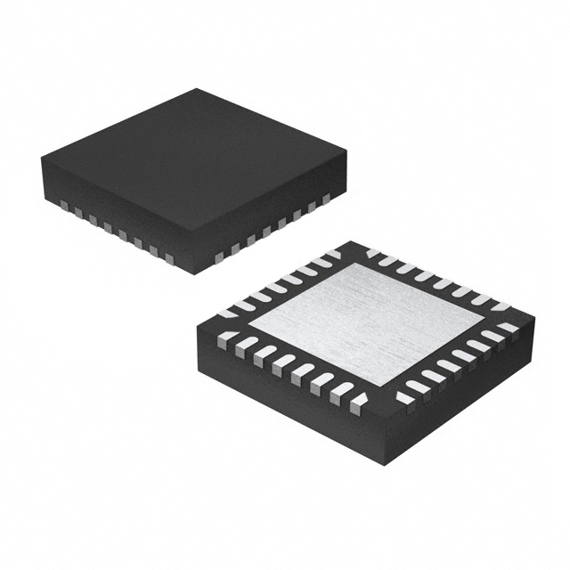
Package
32-pin QFN (5 x 5mm) RoHS
Block Diagram
1) Purchase of IDS-R13MP does not imply any agreement with any third party patent holder or any grant of any ISO14443A or -B licenses.
Customers are solely liable for any infringement of third party’s rights and therefore advised to sign patent licensing agreements with all third
parties! See disclaimer at end of document.
IDS-R13MP_SD-02.doc • June 2009 © IDS Microchip AG
�2•8
IDS-R13MP • 13.56 MHz RFID Reader
Content
1
2
3
4
5
6
7
8
Key Characteristics and Benefits .................................................................................................... 3
Pin Configuration ............................................................................................................................ 3
Short Description ............................................................................................................................ 4
Absolute Maximum Ratings ............................................................................................................ 4
Operating Conditions ...................................................................................................................... 5
Application...................................................................................................................................... 5
Package Outline ............................................................................................................................. 7
Ordering Information....................................................................................................................... 8
Figures
Figure 1: 32-Pin QFN Pinout (Top View) ...................................................................................................................... 3
Figure 2: Matching Circuit (4 ohm to 50 ohm) .............................................................................................................. 5
Figure 3: Typical Application.......................................................................................................................................... 6
1
Related Documents
Specification (full data sheet): IDS-R13MP_DS
IDS-R13MP_SD-02.doc • June 2009 © IDS Microchip AG
�2
IDS-R13MP • 13.56 MHz RFID Reader
3•8
Key Characteristics and Benefits
� Integrated supply voltage regulator for the RF
output stage, providing rejection to supply noise
� High output power (100mW or 200mW) from
single 5V supply
� Antenna driver using OOK or ASK modulation
� Adjustable ASK modulation range (8% to 30%)
� Dual receiver input comprising AM & PM
demodulation ensuring no “communication
holes”
� ISO sub-carrier receiving and decoding
compatibility (212kHz, 424kHz, and 848kHz)
� Built in reception low-pass and high-pass filters
having selectable corner frequencies.
� Selectable reception gain
� Reception automatic gain control
� Reception RSSI measurement for AM and PM
signal (3 bit)
� Measurement of external RF fields for reader to
reader anti-collision
� Self diagnostic of the system through
measurement of RF input level
� Oscillator using 13.56MHz quartz
� Power down, standby and active mode
� Extended temperature range: -40°C to 110°C
� ISO 14443, ISO 15693, Tag-it, ISO14443 high
bit rates, FeliCa and cool-Log™ compatibility
� Integrated low level transmission coding (1 out
of 4, 1 out of 256, modified miller 106Kb/s, NRZ
106Kb/s), Tag-it, FeliCa and cool-Log™
compatible
� Integrated sub-carrier decoders for ISO 15693,
ISO14443 A and B, ISO14443 high bit rates,
Tag-it, Felica and cool-Log™ protocols
� Integrated data framing for ISO 15693,
ISO14443 A and B, ISO14443 high bit rates,
Tag-it, FeliCa and cool-Log™ protocols.
� Integrated CRC and/or parity checking for ISO
15693, ISO14443 A and B, ISO14443 high bit
rates, Tag-it, FeliCa and cool-Log™ protocols
� Parallel 8 bit or serial 4 pin SPI interface with
MCU using 12 bytes FIFO
� Voltage range for communication to MCU
between 1.8V and 5.5V
� Synchronization clock output selectable as RF
frequency, RF/2 or RF/4 frequency
� Operating range from 2.7V to 5.5V
� Integrated supply voltage regulator (20mA)
which can be used to supply MCU and other
external circuitry
3
Pin Configuration
Figure 1: 32-Pin QFN Pinout (Top View)
IDS-R13MP_SD-02.doc • June 2009 © IDS Microchip AG
�4•8
4
IDS-R13MP • 13.56 MHz RFID Reader
Short Description
The IDS-R13MP is an integrated analogue front
end and data framing system for a 13.56MHz RFID
reader system. Built-in programming options make
it suitable for a wide range of applications both in
proximity and vicinity RFID systems.
The reader configuration is achieved by selecting
the desired protocol in the control registers. Direct
access to all control registers also allows finetuning of different reader parameters if needed.
Parallel or serial interface can be selected for
communication between MCU and reader. When
hardware coders and decoders are used
(accelerators for different standards), transmission
and receive function use the 12-bytes FIFO
register. In case of direct transmission or reception,
coders and decoders are bypassed and MCU has
to service reader in real time.
The transmitter generates 100mW or 200mW
output power into 50� load (at 5V supply) and is
capable of OOK or ASK modulation. The integrated
supply voltage regulators ensure supply rejection of
the complete reader system.
The transmission system comprises low level
coding for 1 out of 4 and 1 out of 256 for ISO15693,
modified Miller for ISO14443A and high bit rate
systems, Tag-it™ encoding. For all these systems
5
the automatic generation of SOF and EOF, CRC
and/or parity is supported.
The receiver system enables AM and PM
demodulation using a dual input system (patent
pending). The receiver also comprises automatic
gain control option (also patent pending) and
selectable gain and signal bandwidth to cover a
range of input sub-carriers signal options. The
signal strength of AM and PM modulation is
measured and can be accessed in RSSI register.
The receiver output is selectable between digitized
sub-carrier signal and any of eleven integrated
sub-carrier decoders (two for ISO 15693 high bit
rate, two for ISO15693 low bit rate, two for ISO
14443, three for ISO14443 high bit rates, one for
Tag-it™ system). Selected decoders deliver bit
stream and data clock as outputs.
The receiver system also comprises framing
system. This system performs the CRC and/or
parity check, removes the EOF and SOF strings
and organizes the data in bytes. Framed data is
accessible to MCU through a 12-byte FIFO register
and MCU interface. The framing is supported for
ISO15693 and ISO14443.
To support external MCU and other circuitry a 3.3V
regulated supply output and synchronization clock
output are available. The regulated supply has a
source current capability of 20mA.
Absolute Maximum Ratings
(Operating free–air temperature range, unless otherwise noted)*
Supply Voltage Range VEXT (see Note 1)................................................................................................................... -0.3 V to 6 V
Maximum Positive Voltage - Other Pads..................................................................................................................... VSUP + 0.3V
Maximum Negative Voltage - Other Pads ..............................................................................................................................-0.3V
ESDS Rating, HBM (Human Body Model) .............................................................................................................................. 2 kV
ESDS Rating, CDM (Charged Device Model)........................................................................................................................ 500V
ESDS Rating, MM (Machine Model)....................................................................................................................................... 200V
Maximum Operating Virtual Junction Temperature, TJ ....................................................................................................... 140°C
Storage Temperature, Tstg .................................................................................................................................... -55°C to +150°C
Lead Temperature 1.6 mm from case for 10 seconds......................................................................................................... 300ºC
*Stresses beyond those listed under »Absolute Maximum Ratings« may cause permanent damage to the device. These are
stress ratings only and functional operation of the device at these or any other conditions beyond those indicated under
»Operating Conditions« are not implied. Exposure to absolute-maximum-rated conditions for extended periods may affect
device reliability.
NOTE 1: All voltage values are with respect to substrate ground terminal VSS.
IDS-R13MP_SD-02.doc • June 2009 © IDS Microchip AG
�IDS-R13MP • 13.56 MHz RFID Reader
6
5•8
Operating Conditions
(Operating free–air temperature range)
External Positive Supply Voltage, VEXT .................................................................................................... 2.7V to 5.5V, 5V typical
Operating virtual junction temperature range, TJ .................................................................................................-40°C to +125°C
Operating ambient temperature range, TA ...........................................................................................................-40°C to +110°C
Input Current at Any Pin ..................................................................................................................................................... ±100mA
Input Voltage at Analogue Input Pins ....................................................................................................1.5VP (MAX) (single-ended)
7
Application
Figure 2 shows a typical matching
circuit for 50 ohm.
Figure 3 shows a typical
application (4 ohm) with USB
interface.
Figure 2: Matching Circuit (4 ohm to 50 ohm)
IDS-R13MP_SD-02.doc • June 2009 © IDS Microchip AG
�6•8
IDS-R13MP • 13.56 MHz RFID Reader
Figure 3: Typical Application
IDS-R13MP_SD-02.doc • June 2009 © IDS Microchip AG
�IDS-R13MP • 13.56 MHz RFID Reader
8
7•8
Package Outline
32-Pin QFN
All dimensions are in millimetres.
Description
Legend
Package Size
Lead
Pitch
Lead
Width
Overall
Height
StandOff
Lead
Height
D
E
e
b
L
D2
E2
A
A1
A3
5.00
5.00
0.50
0.25
0.40
3.45
3.45
0.90
0.02
0.20
Min.
0.18
0.30
3.30
3.30
0.80
0.00
Max.
0.30
0.50
3.55
3.55
1.00
0.05
Nom.
IDS-R13MP_SD-02.doc • June 2009 © IDS Microchip AG
�8•8
9
IDS-R13MP • 13.56 MHz RFID Reader
Ordering Information
ORDERING
CODE
IDS-R13MP
DESCRIPTION
OPERATING
TEMPERATURE RANGE
PACKAGE
TYPE
DEVICE
MARKING
SHIPPING
FORM
-40°C to 110°C
QFN32
(5 x 5 mm)
RoHS*
IDS
R13MP
Mini Tape & Reel
(250/reel)
13.56 MHz Multi-Protocol
RFID Reader IC
*) Pb-Free (RoHS compatible), and free of Bromine (Br) and Antimony (Sb) based flame retardants (Br or Sb do not exceed 0.1% by
weight in homogeneous material).
Order quantities should be a multiple of shipping form.
Sales & Marketing Office
IDS Microchip AG
Sales & Marketing Americas
IC Magic Inc.
Wächlenstrasse 5,
CH-8832 Wollerau, Switzerland
Phone: +41 43 844 6253
Fax: +41 43 844 6250
sales@ids-microchip.com
34 Granlea Rd,
North York, ON M2N 2Z5, Canada
Phone: +416 227 9196
Fax: +41 43 844 6250
sales@ic-magic.com
www.ids-microchip.com
cool-Log™ is a registered trademark of IDS Microchip AG.
Tag-it™ is a registered trademark of Texas Instruments, Inc.
IDS reserves the right to change or discontinue such products without notice.
The information furnished here by IDS is believed to be correct and accurate as of the publication date. However, IDS shall not be liable to any third party for any damages, including but
no limited to personal injury, property damage, loss of profits, loss of use, interruption of business or indirect, special, incidental, or consequential damages of any kind in connection with
or arising out of the furnishing, performance, or use of the technical data. No obligation or liability to any third party shall arise or flow out of IDS' rendering technical or other services.
Products sold by IDS are covered exclusively by the IDS standard warranty, patent indemnification, and other provisions appearing in IDS standard "Terms of Sale". Testing and other
quality control techniques are used to the extent IDS deems necessary to support this warranty. Except where mandated by government requirements, testing of all parameters of each
product is not necessarily performed. IDS makes no warranty (express, statutory, implied and/or by description), including without limitation any warranties of merchantability and/or
fitness for a particular purpose, regarding the information set forth in the Materials pertaining to IDS products, or regarding the freedom of any products described in the Materials from
patent and/or other infringement. Purchase of IDS-R13MP does not imply any agreement with any third party patent holder or any grant of any ISO14443A or -B licenses. Customers are
solely liable for any infringement of third party’s rights and therefore advised to sign patent licensing agreements with all third parties!
IDS reserves the right to discontinue production and change specifications and prices, make corrections, modifications, enhancements, improvements and other changes of its products
and services at any time without notice. IDS products are intended for use in commercial applications. Applications requiring extended temperature range, unusual environmental
requirements, or high reliability applications, such as military, medical life-support or life-sustaining equipment, are specifically not recommended without additional mutually agreed upon
processing by IDS for such applications. IDS assumes no liability for application assistance or customer product design. Customers are responsible for their products and applications
using IDS components.
IDS-R13MP_SD-02.doc • June 2009 © IDS Microchip AG
�


 工商网监
湘ICP备2023018690号
工商网监
湘ICP备2023018690号