Product Specifications
PART NO.:
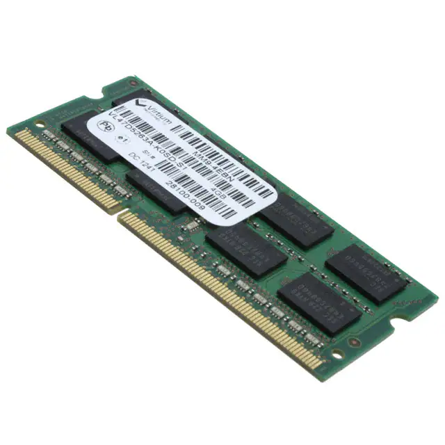
VL47D5263A-K0SD-S1
REV: 1.0
General Information
4GB 512Mx64 DDR3 SDRAM LOW VOLTAGE NON-ECC UNBUFFERED SODIMM 204-PIN
Description
The VL47D5263A is a 512Mx64 DDR3 SDRAM high density SODIMM. This dual rank memory module consists of
sixteen CMOS 256Mx8 bits with 8 banks DDR3 synchronous DRAMs in BGA packages and a 2K EEPROM with
thermal sensor in an 8-pin MLF package. This module is a 204-pin small-outline dual in-line memory module and is
intended for mounting into an edge connector socket. Decoupling capacitors are mounted on the printed circuit board
for each DDR3 SDRAM.
Features
•
•
•
•
•
•
•
•
•
•
•
•
•
•
•
•
•
•
•
•
•
•
Pin Description
204-pin, small-outline dual in-line memory module (SODIMM)
Fast data transfer rate: PC3-12800
VDD = VDDQ = 1.35V (1.28V~1.45V) & 1.5V (1.425V~1.575V)
JEDEC standard 1.35V (1.28V~1.45V) & 1.5V (1.425V~1.575V)
VDDSPD = 3.0V to 3.6V
Eight internal component banks for concurrent operation
8-bit pre-fetch architecture
Bi-directional differential data-strobe
Nominal and dynamic on-die termination (ODT)
ZQ calibration support
Programmable CAS# latency: 11 (DDR3-1600)
Programmable burst; length (8)
Average refresh period 7.8 us
Asynchronous reset
Fly-by topology
On board terminated command, address, and control bus
Serial presence detect (SPD) EEPROM with thermal sensor
o
o
o
Thermal sensor range: -40 C to +125 C (Max +/-3 C accuracy)
Lead-free, RoHS compliant
Gold edge contacts
PCB: Height 30.00mm (1.181”), double sided component
o
o
Operating temperature (TOPER): -40 C to +95 C (module screening using
commercial DRAM)
o
Function
A0~A14
Address Inputs
A10/AP
Address Input/ Autoprecharge
A12/BC#
Address Input/ Burst Chop
BA0~BA2
Bank Address Inputs
DQ0~DQ63
Data Input/Output
DQS0~DQS7
Data Strobes
DQS0#~DQS7#
Data Strobes Complement
DM0~DM7
Data Masks
CK0,CK0#,
CK1,CK1#
Clock Input
ODT0, ODT1
On-die Termination Control
CKE0, CKE1
Clock Enables
CS0#, CS1#
Chip Selects
RAS#
Row Address Strobes
CAS#
Column Address Strobes
WE#
Write Enable
VDD
Voltage Supply
VSS
Ground
SA0~SA1
SPD Address
SDA
SPD Data Input/Output
SCL
SPD Clock Input
EVENT#
Temperature Event Output
VREFCA
Reference Voltage for CA
VREFDQ
Reference Voltage for DQ
VDDSPD
SPD Voltage Supply
VTT
Termination Voltage
RESET#
Register and SDRAM Control
NC
No Connect
o
Notes: Double refresh rate is required when 85 C < TOPER
很抱歉,暂时无法提供与“VL-MM9-4EBN”相匹配的价格&库存,您可以联系我们找货
免费人工找货