Product Specifications
PART NO.:
VL470L2925-R3SG
REV: 1.0
General Information
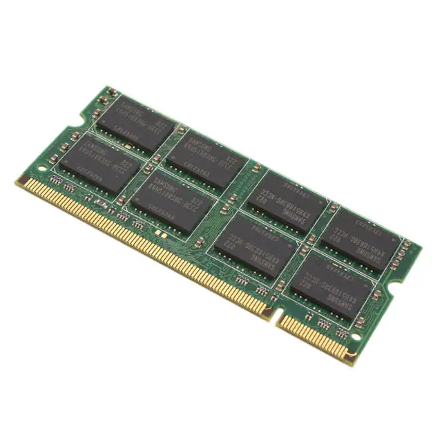
1GB 128Mx64 DDR SDRAM NON-ECC UNBUFFERED SODIMM 200-PIN
Description
The VL470L2925 is a 128Mx64 Double Data Rate SDRAM high density SODIMM. This dual rank memory module
consists of sixteen CMOS 64Mx8 bits with 4 banks Synchronous DRAMs in BGA packages and a 2K EEPROM in an
8-pin TSSOP package. This module is a 200-pin small-outline dual in-line memory module and is intended for
mounting into an edge connector socket. Decoupling capacitors are mounted on the printed circuit board for each
DDR SDRAM.
Features
•
•
•
•
•
•
•
•
•
•
•
•
•
•
•
•
•
•
Pin Description
200-pin, small-outline dual in-line memory module (SODIMM)
Two data transfers per clock cycle
VDD = VDDQ = 2.5V +/-0.2V for DDR333
JEDEC standard 2.5V I/O (SSTL_2 compatible)
VDDSPD = 2.3V to 3.6V
Bi-directional data-strobe (DQS)
Differential clock inputs (CK and CK#)
DLL aligns DQ and DQS transition with CK transition
Programmable read latency: DDR333 (2.5 clock)
Programmable burst; length (2, 4, 8)
Programmable burst (sequential & interleave)
Auto & Self refresh, 7.8us refresh interval (8K/64ms refresh)
Serial presence detect (SPD) with EEPROM
Lead-free, RoHS compliant
JEDEC pinout
Gold edge contacts
PCB: Height 31.75mm (1.250”), double sided component
o
Operating temperature (TA): -40 to +85 C (module screening using
commercial DRAM)
Order Information:
VL470L2925 - R3 S G
DRAM DIE
G-DIE
Pin Name
Function
A0~A12
Row Address Inputs
A0~A9, A11
Column Address Inputs
BA0~BA1
Bank Address Inputs
DQ0~DQ63
Data Input/Output
DQS0~DQS7
Data Strobes Input/Output
DM0~DM7
Data Mask
CK0, CK0#
CK1, CK1#
Clock Input
CKE0, CKE1
Clock Enables Input
CS0#, CS1#
Chip Selects Input
RAS#
Row Address Strobes
CAS#
Column Address Strobes
WE#
Write Enable
VDD
Voltage Supply
VDDQ
Voltage Supply for DQS
VSS
Ground
VREF
Power Supply Reference
VDDSPD
SPD Voltage Supply
SA1~SA2
SPD Address
SDA
SPD Data Input/Output
SCL
SPD Clock Input
NC
No Connect
DRAM MANUFACTURER
S - SAMSUNG
MODULE SPEED
R3: PC2700 @CL2.5
(R: Screening grade)
VL: Lead-free/RoHS
DRAM component: Samsung K4H510838G-HCB3
Tel 949.888.2444 – 30052 Tomas, Rancho Santa Margarita, CA 92688 USA – www.virtium.com
1
�Product Specifications
PART NO.:
VL470L2925-R3SG
REV: 1.0
Pin Configuration
200-PIN DDR SODIMM FRONT
200-PIN DDR SODIMM BACK
Pin
Name
Pin
Name
Pin
Name
Pin
Name
Pin
Name
Pin
Name
Pin
Name
Pin
Name
1
VREF
51
VSS
101
A9
151
DQ42
2
VREF
52
VSS
102
A8
152
DQ46
3
VSS
53
DQ19
103
VSS
153
DQ43
4
VSS
54
DQ23
104
VSS
154
DQ47
5
DQ0
55
DQ24
105
A7
155
VDD
6
DQ4
56
DQ28
106
A6
156
VDD
7
DQ1
57
VDD
107
A5
157
VDD
8
DQ5
58
VDD
108
A4
158
CK1#
9
VDD
59
DQ25
109
A3
159
VSS
10
VDD
60
DQ29
110
A2
160
CK1
11
DQS0
61
DQS3
111
A1
161
VSS
12
DM0
62
DM3
112
A0
162
VSS
13
DQ2
63
VSS
113
VDD
163
DQ48
14
DQ6
64
VSS
114
VDD
164
DQ52
15
VSS
65
DQ26
115
A10
165
DQ49
16
VSS
66
DQ30
116
BA1
166
DQ53
17
DQ3
67
DQ27
117
BA0
167
VDD
18
DQ7
68
DQ31
118
RAS#
168
VDD
19
DQ8
69
VDD
119
WE#
169
DQS6
20
DQ12
70
VDD
120
CAS#
170
DM6
21
VDD
71
CB0*
121
CS0#
171
DQ50
22
VDD
72
CB4*
122
CS1#
172
DQ54
23
DQ9
73
CB1*
123
NC
173
VSS
24
DQ13
74
CB5*
124
CS2#*
174
VSS
25
DQS1
75
VSS
125
VSS
175
DQ51
26
DM1
76
VSS
126
VSS
176
DQ55
27
VSS
77
DQS8*
127
DQ32
177
DQ56
28
VSS
78
DM8*
128
DQ36
178
DQ60
29
DQ10
79
CB2*
129
DQ33
179
VDD
30
DQ14
80
CB6*
130
DQ37
180
VDD
31
DQ11
81
VDD
131
VDD
181
DQ57
32
DQ15
82
VDD
132
VDD
182
DQ61
33
VDD
83
CB3*
133
DQS4
183
DQS7
34
VDD
84
CB7*
134
DM4
184
DM7
35
CK0
85
CS3#* 135
DQ34
185
VSS
36
VDD
86
NC
136
DQ38
186
VSS
37
CK0#
87
VSS
137
VSS
187
DQ58
38
VSS
88
VSS
138
VSS
188
DQ62
39
VSS
89
CK2*
139
DQ35
189
DQ59
40
VSS
90
VSS
140
DQ39
190
DQ63
41
DQ16
91
CK2#*
141
DQ40
191
VDD
42
DQ20
92
VDD
142
DQ44
192
VDD
43
DQ17
93
VDD
143
VDD
193
SDA
44
DQ21
94
VDD
144
VDD
194
SA0
45
VDD
95
CKE1
145
DQ41
195
SCL
46
VDD
96
CKE0
146
DQ45
196
SA1
47
DQS2
97
NC
147
DQS5
197
VDDSPD
48
DM2
98
NC
148
DM5
198
SA2
49
DQ18
99
A12
149
VSS
199
NC
50
DQ22
100
A11
150
VSS
200
NC
Note: *: These pins are not used in this module.
Tel 949.888.2444 – 30052 Tomas, Rancho Santa Margarita, CA 92688 USA – www.virtium.com
2
�Product Specifications
PART NO.:
VL470L2925-R3SG
REV: 1.0
Function Block Diagram
CS1#
CS0#
DQS0
DQS4
DM0
DQ0
DQ1
DQ2
DQ3
DQ4
DQ5
DQ6
DQ7
DM4
DM
DQ0
DQ1
DQ2
DQ3
DQ4
DQ5
DQ6
DQ7
CS# DQS
D0
DM
DQ0
DQ1
DQ2
DQ3
DQ4
DQ5
DQ6
DQ7
CS# DQS
DQ32
DQ33
DQ34
DQ35
DQ36
DQ37
DQ38
DQ39
D8
DQS1
CS# DQS
D1
DM
DQ0
DQ1
DQ2
DQ3
DQ4
DQ5
DQ6
DQ7
CS# DQS
DQ40
DQ41
DQ42
DQ43
DQ44
DQ45
DQ46
DQ47
D9
CS# DQS
D2
DM
DQ0
DQ1
DQ2
DQ3
DQ4
DQ5
DQ6
DQ7
CS# DQS
DQ48
DQ49
DQ50
DQ51
DQ52
DQ53
DQ54
DQ55
D10
CS# DQS
DM
DQ0
DQ1
DQ2
DQ3
DQ4
DQ5
DQ6
DQ7
CS# DQS
CS# DQS
D5
DM
DQ0
DQ1
DQ2
DQ3
DQ4
DQ5
DQ6
DQ7
CS# DQS
DM
DQ0
DQ1
DQ2
DQ3
DQ4
DQ5
DQ6
DQ7
CS# DQS
D13
D6
D14
DQS7
DM3
A0~A12
DM
DQ0
DQ1
DQ2
DQ3
DQ4
DQ5
DQ6
DQ7
DM
DQ0
DQ1
DQ2
DQ3
DQ4
DQ5
DQ6
DQ7
D12
DM6
DM
DQ0
DQ1
DQ2
DQ3
DQ4
DQ5
DQ6
DQ7
DQS3
BA0~BA1
CS# DQS
CS# DQS
DQS6
DM2
DQ24
DQ25
DQ26
DQ27
DQ28
DQ29
DQ30
DQ31
DM
DQ0
DQ1
DQ2
DQ3
DQ4
DQ5
DQ6
DQ7
D4
DM
DQ0
DQ1
DQ2
DQ3
DQ4
DQ5
DQ6
DQ7
DM5
DM
DQ0
DQ1
DQ2
DQ3
DQ4
DQ5
DQ6
DQ7
DQS2
DQ16
DQ17
DQ18
DQ19
DQ20
DQ21
DQ22
DQ23
CS# DQS
DQS5
DM1
DQ8
DQ9
DQ10
DQ11
DQ12
DQ13
DQ14
DQ15
DM
DQ0
DQ1
DQ2
DQ3
DQ4
DQ5
DQ6
DQ7
DM7
DM
DQ0
DQ1
DQ2
DQ3
DQ4
DQ5
DQ6
DQ7
CS# DQS
D3
DM
DQ0
DQ1
DQ2
DQ3
DQ4
DQ5
DQ6
DQ7
CS# DQS
DQ56
DQ57
DQ58
DQ59
DQ60
DQ61
DQ62
DQ63
D11
Serial PD
BA0~BA1: DDR SDRAMs D0~D15
A0~A12: DDR SDRAMs D0~D15
RAS#
RAS#: DDR SDRAMs D0~D15
CAS#
CAS#: DDR SDRAMs D0~D15
WE#
WE#: DDR SDRAMs D0~D15
CKE0
CKE0: DDR SDRAMs D0~D7
CKE1
CKE0: DDR SDRAMs D8~D15
SDA
Vss
A0
A1
A2
SA0 SA1 SA2
Clock Input
CK0, CK0#
CK1, CK1#
DDR SDRAMs
8 SDRAMs
8 SDRAMs
VDDSPD
VDD/ VDDQ
Notes:
1. Unless otherw ise noted, resistor values are 22 ohms +/-5%
D15
Clock Wiring
SCL
WP
D7
Serial PD
D0-D15
VREF
D0-D15
VSS
D0-D15
Tel 949.888.2444 – 30052 Tomas, Rancho Santa Margarita, CA 92688 USA – www.virtium.com
3
�Product Specifications
PART NO.:
VL470L2925-R3SG
REV: 1.0
Absolute Maximum Ratings
Symbol
Parameter
Value
Unit
VIN, VOUT
Voltage on any pin relative to VSS
-0.5 ~ 3.6
V
VDD, VDDQ
Voltage on VDD & VDDQ supply relative to VSS
-1.0 ~ 3.6
V
Storage temperature
-55 ~ +150
0
-40 ~ +85
0
TSTG
C
TA
Operating temperature
C
PD
Power dissipation
16
W
IOS
Short circuit current
50
mA
Notes:
Permanent device damage may occur if ABSOLUTE MAXIMUM RATINGS are exceeded.
Functional operation should be restricted to recommended operating condition.
Exposure to higher than recommended voltage for extended periods of time could affect device reliability.
DC Operating Conditions
Alls voltages referenced to VSS
TA = -400C to +850C
Symbol
VDD
Parameter
Supply voltage
VDDQ
I/O Supply voltage
VREF
I/O Reference voltage
Min
Max
Unit
2.3
2.7
V
2.3
2.7
V
0.49 * VDDQ
0.51 * VDDQ
V
1
2
VTT
I/O Termination voltage
VREF-0.04
VREF+0.04
V
VIH(DC)
Input logic high voltage
VREF+0.15
VDDQ+0.30
V
VIL(DC)
Input logic low voltage
-0.3
VREF-0.15
V
VIN(DC)
Input voltage level, CK and CK#
-0.3
VDDQ+0.30
V
VID(DC)
Input differential voltage, CK and CK#
0.3
VDDQ+0.60
V
VIX(DC)
Input crossing point voltage, CK and CK#
0.3
VDDQ+0.60
V
Address, CAS#,RAS#,WE#
-32
32
uA
CS#,CKE
-16
16
uA
CK, CK#
-16
16
uA
II
Input leakage current
DM
-4
4
uA
-10
10
uA
Output high current(normal strength) VOUT = v + 0.84V
-16.8
-
mA
IOZ
Output leakage current
IOH
Note
IOL
Output high current(normal strength) VOUT = VTT - 0.84V
16.8
-
mA
IOH
Output high current(half strength) VOUT = VTT + 0.45V
-9
-
mA
IOL
Output high current(half strength) VOUT = VTT - 0.45V
9
-
mA
3
Notes:
1. VREF is expected to be equal to 0.5*VDDQ of the transmitting device, and to track variations in the DC level of the same.
Peak to peak noise on VREF may not exceed +/- 2% of the DC value.
2. VTT is not applied directly to the device. VTT is a system supply for signal termination resistors, is expected to be set equal to
VREF, and must track variations in the DC level of VREF.
3. VID is the magnitude of the difference between the input level on CK and the input level of CK#.
Tel 949.888.2444 – 30052 Tomas, Rancho Santa Margarita, CA 92688 USA – www.virtium.com
4
�Product Specifications
PART NO.:
VL470L2925-R3SG
REV: 1.0
AC Operating Conditions
All voltages referenced to VSS
TA = -400C to +850C
Symbol
Parameter
Min
Max
Unit
VIH(AC)
Input High (Logic 1) Voltage
VREF + 0.31
-
V
VIL(AC)
Input Low (Logic 0) Voltage
-
VREF - 0.31
V
VID(AC)
Input Differential Voltage, CK and CK# inputs
0.70
VDDQ + 0.60
V
VIX(AC)
Input Crossing Point Voltage, CK and CK# inputs
0.5*VDDQ - 0.2
0.5*VDDQ + 0.2
V
Input/Output
Capacitance
0
TA=25 C, f=100MHz
Parameter
Symbol
Min
Max
Unit
Input capacitance (A0~A12, BA0~BA1, RAS#, CAS#, WE#)
CIN1
28
44
pF
Input capacitance (CKE0, CKE1)
CIN2
16
24
pF
Input capacitance (CS0#, CS1#)
CIN3
16
24
pF
Input capacitance (CK0, CK0#, CK1, CK1#)
CIN4
16
24
pF
Input/Output capacitance (DQ, DQS, DQS#, DM)
CIO
11
13
pF
Tel 949.888.2444 – 30052 Tomas, Rancho Santa Margarita, CA 92688 USA – www.virtium.com
5
�Product Specifications
PART NO.:
VL470L2925-R3SG
REV: 1.0
IDD Specification
Condition
Symbol
B3
(DDR333)
Unit
OPERATING CURRENT: One device bank active; Active-Precharge; tRC=tRC(MIN);
tCK=tCK(MIN); DQ,DM and DQS inputs change once per clock cycle; Address and
control inputs change once every two clock cycles
IDD0*
560
mA
OPERATING CURRENT: One device bank; Active-Read-Precharge; BL=4;
tRC=tRC(MIN); tCK=tCK(MIN); IOUT =0mA; Address and control inputs change once
per clock cycle
IDD1*
680
mA
PRECHARGE POWER-DOWN STANDBY CURRENT: All device banks are idle;
Power-down mode; tCK=tCK(MIN); CKE=LOW
IDD2P**
80
mA
IDLE STANDBY CURRENT: CS#=HIGH; All device banks are idle; tCK=tCK(MIN);
CKE=HIGH; Address and other control inputs changing once per clock cycle.
VIN =VREF for DQ,DQS and DM
IDD2F**
368
mA
IDD3P**
240
mA
ACTIVE STANDBY CURRENT: CS#=HIGH; CKE=HIGH; One device bank active;
tRC =tRAS(MAX); tCK=tCK(MIN); DQ, DM and DQS inputs change twice per clock
cycle; Address and other control inputs changing once per clock cycle
IDD3N**
640
mA
OPERATING CURRENT: Burst = 2; Reads; Continnuous burst; One device bank
active; Address and other control inputs changing once per clock cycle;
tCK=tCK(MIN); IOUT=0mA
IDD4R*
800
mA
OPERATING CURRENT: Burst = 2; Writes; Continnuous burst; One device bank
active; Address and other control inputs changing once per clock cycle;
tCK=tCK(MIN); DQ, DM and DQS inputs change twice per clock cycle
IDD4W*
840
mA
AUTO REFRESH CURRENT: tRC=tRFC(MIN)
IDD5**
1760
mA
SELF-REFRESH CURRENT: CKE< 0.2V
IDD6**
80
mA
OPERATING CURRENT: Four device bank interleaving Reads Burst=4 with auto
precharge; tRC=tRC(MIN); tCK=tCK(MIN); Address and control inputs change only
during Active READ, or WRITE commands
IDD7*
1800
mA
ACITVE POWER-DOWN STANDBY CURRENT: One device bank active; Powerdown mode; tCK=tCK(MIN); CKE=LOW
Notes:
IDD specification is based on Samsung G-die components. Other manufacturers' DRAMs may have different values.
*: Value calculated as one module rank in this operation condition, and other module rank in IDD2P (CKE LOW) mode.
**: Value calculated as all module ranks in this operation condition.
Tel 949.888.2444 – 30052 Tomas, Rancho Santa Margarita, CA 92688 USA – www.virtium.com
6
�Product Specifications
PART NO.:
VL470L2925-R3SG
REV: 1.0
AC TIMING PARAMETERS & SPECIFICATIONS
Parameter
Symbol
Row cycle time
Refresh row cycle time
Row active time
RAS to CAS delay
Row precharge time
Row active to Row active delay
Write recovery time
Last data in to Read command
tRC
tRFC
tRAS
tRCD
tRP
tRRD
tWR
tWTR
Clock cycle time
CL=2.0
CL=2.5
CL=3.0
Clock high level width
Clock low level width
DQS-out access time from CK/CK
Output data access time from CK/CK
Data strobe edge to ouput data edge
Read Preamble
Read Postamble
CK to valid DQS-in
DQS-in setup time
DQS-in hold time
DQS falling edge to CK rising-setup time
DQS falling edge from CK rising-hold time
DQS-in high level width
DQS-in low level width
Address and Control Input setup time(fast)
Address and Control Input hold time(fast)
Address and Control Input setup time(slow)
Address and Control Input hold time(slow)
Data-out high impedence time from CK/CK
Data-out low impedence time from CK/CK
Mode register set cycle time
DQ & DM setup time to DQS
DQ & DM hold time to DQS
Control & Address input pulse width
DQ & DM input pulse width
Exit self refresh to non-Read command
Exit self refresh to read command
Refresh interval time
Output DQS valid window
Clock half period
Data hold skew factor
DQS write postamble time
Active to Read with Auto precharge
command
Autoprecharge write recovery + Precharge
time
Power Down Exit Time
tCK
tCH
tCL
tDQSCK
tAC
tDQSQ
tRPRE
tRPST
tDQSS
tWPRES
tWPRE
tDSS
tDSH
tDQSH
tDQSL
tIS
tIH
tIS
tIH
tHZ
tLZ
tMRD
tDS
tDH
tIPW
tDIPW
tXSNR
tXSRD
tREFI
tQH
tHP
tQHS
tWPST
tRAP
tDAL
tPDEX
CC
(DDR400)
Min
Max
55
70
40
70K
15
15
10
15
2
6
12
5
10
0.45
0.55
0.45
0.55
-0.55
+0.55
-0.65
+0.65
0.4
0.9
1.1
0.4
0.6
0.72
1.28
0
0.25
0.2
0.2
0.35
0.35
0.6
0.6
0.7
0.7
-0.65
+0.65
-0.65
+0.65
10
0.4
0.4
2.2
1.75
75
200
7.8
tHP
-tQHS
tCLmin
or tCHmin
0.5
0.4
0.6
B3
(DDR333)
Min
Max
60
72
42
70K
18
18
12
15
1
7.5
12
6
12
0.45
0.55
0.45
0.55
-0.6
+0.6
-0.7
+0.7
0.4
0.9
1.1
0.4
0.6
0.75
1.25
0
0.25
0.2
0.2
0.35
0.35
0.75
0.75
0.8
0.8
-0.7
+0.7
-0.7
+0.7
12
0.45
0.45
2.2
1.75
75
200
7.8
tHP
-tQHS
tCLmin
or tCHmin
0.55
0.4
0.6
B0
(DDR266)
Min
Max
65
75
45
120K
20
20
15
15
1
10
12
7.5
12
0.45
0.55
0.45
0.55
-0.75
+0.75
-0.75
+0.75
0.5
0.9
1.1
0.4
0.6
0.75
1.25
0
0.25
0.2
0.2
0.35
0.35
0.9
0.9
1.0
1.0
-0.75
+0.75
-0.75
+0.75
15
0.5
0.5
2.2
1.75
75
200
7.8
tHP
-tQHS
tCLmin
or tCHmin
0.75
0.4
0.6
15
18
20
(tWR/tCK)
+
(tRP/tCK)
1
(tWR/tCK)
+
(tRP/tCK)
1
(tWR/tCK)
+
(tRP/tCK)
1
Tel 949.888.2444 – 30052 Tomas, Rancho Santa Margarita, CA 92688 USA – www.virtium.com
Unit
ns
ns
ns
ns
ns
ns
ns
tCK
ns
tCK
tCK
ns
ns
ns
tCK
tCK
tCK
ns
tCK
tCK
tCK
tCK
tCK
ns
ns
ns
ns
ns
ns
ns
ns
ns
ns
ns
ns
tCK
us
ns
ns
ns
tCK
tCK
tCK
7
�Product Specifications
PART NO.:
VL470L2925-R3SG
REV: 1.0
Package Dimensions
FRONT VIEW
3.40
MAX
67.60
4.0 +/- 0.10 (2X)
31.75
1.80 (2X)
TYP
20.00
6.00 TYP
0.5 R
PIN 1
2.15 TYP
1.00 +/- 0.10
0.60 TYP
1.0 +/- 0.10
PIN 199
0.45 TYP
63.60 TYP
BACK VIEW
3.50 TYP
2.55 TYP
4.20 TYP
PIN 200
47.40
TYP
11.40
TYP
15.35
TYP
PIN 2
Note: 1. All dimensions are in millimeters with tolerance +/- 0.15mm unless otherwise specified.
2. The dimensional diagram is for reference only.
Tel 949.888.2444 – 30052 Tomas, Rancho Santa Margarita, CA 92688 USA – www.virtium.com
8
�Product Specifications
PART NO.:
VL470L2925-R3SG
REV: 1.0
Revision History:
Date
10/24/2014
Rev.
Page
1.0
All
Changes
Spec release
Tel 949.888.2444 – 30052 Tomas, Rancho Santa Margarita, CA 92688 USA – www.virtium.com
9
�