SEA & LAND ELECTRONIC CORP.
WWW.SEALAND-PPTC.COM
ALPHA-TOP TECHNOLOGY CORP.
WWW.ALPHA-TOP.COM
APPROVAL SHEET
MODEL NO.:
SMD1210 Series
CUSTOMER:
CUSTOMER'S APPROVAL:
AUTHORIZED SIGNATURE/STAMP:
DATE
MANUFACTURER:
HEAD OFFICE:
China Branch:
Submitted by:
Approved by:
DATE:
13F.,No.120-10,Sec.3,Zhongshan Rd.,Zhonghe Dist.,New Taipei City 23544,Taiwan
Tel: 886-2-8221-2567
Fax:882-2-2225-7268
E-mail:service@chipfast.com.tw
31 Chang-Xin-Zon Road,Gao-Ling lndustrial Zone,Chiu-chang Town,
Huey Yang Distric,Huey Zhou City,Guang Dong516221,CHINA
Tel: 86-752-3562001
Fax:86-752-3558696
E-mail:service@atpptc.com
Chung Cheng
YC Lin
2-Mar-22
SEA & LAND ELECTRONIC CORP.
第 1页
�Features
Applications
■ Surface Mount Devices
Almost anywhere there is a low voltage
■ Lead free device
power supply, up to 30V and a load to be
■ Size 3.2*2.5mm/0.12*0.10 inch
protected, including:
■ Surface Mount packaging
■ Computer mother board, Modem.
for automated assembly
■ Telecommunication equipments.
SMD1210 Series
Alpha-Top (Sea&Land Alliance)
Performance Specification
Vmax
Imax
Ihold
Itrip
Pd
Model
Marking
@25°C
@25°C
Typ.
(Vdc)
(A)
(A)
(A)
(W)
SMD1210-005
30
100
0.05
0.15
0.6
αA
SMD1210-010
30
100
0.10
0.30
0.6
αB
SMD1210-020
30
100
0.20
0.40
0.6
αC
SMD1210-035
6
100
0.35
0.75
0.6
αD
SMD1210-050
13.2
100
0.50
1.00
0.6
αF
SMD1210-075
6
100
0.75
1.50
0.6
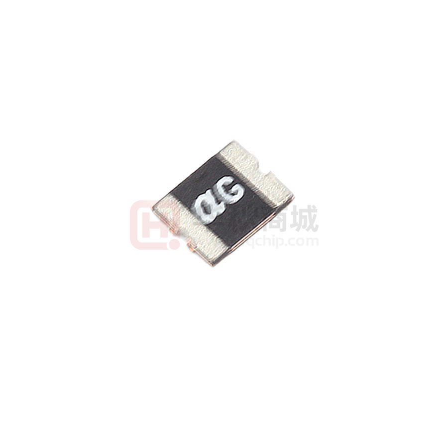
αG
SMD1210-110
6
100
1.10
2.20
0.6
αH
SMD1210-150
6
100
1.50
3.00
0.6
αL
SMD1210-175
6
100
1.75
3.50
0.8
αN
SMD1210-200
6
100
2.00
4.00
0.8
αS
Ihold = Hold Current. Maximum current device will not trip in 25°C still air.
Itrip = Trip Current. Minimum current at which the device will always trip in 25°C still air.
Vmax = Maximum operating voltage device can withstand without damage at rated current (Imax).
Imax = Maximum fault current device can withstand without damage at rated voltage (Vmax).
Pd
= Power dissipation when device is in the tripped state in 25°C still air environment at rated voltage.
Rimin/max = Minimum/Maximum device resistance prior to tripping at 25°C.
R1max = Maximum device resistance is measured one hour post reflow.
CAUTION : Operation beyond the specified ratings may result in damage and possible arcing and flame.
Maximum
Time To Trip
Current
Time
(A)
(Sec)
0.25
1.50
0.50
0.60
8.0
0.02
8.0
0.20
8.0
0.10
8.0
0.10
8.0
0.30
8.0
0.50
8.0
0.60
8.0
1.00
Environmental Specifications
Test
Conditions
Passive aging
+85°C, 1000 hrs.
Humidity aging
+85°C, 85% R.H. , 168 hours
Thermal shock
+85°C to -40°C, 20 times
Resistance to solvent
MIL-STD-202,Method 215
Vibration
MIL-STD-202,Method 201
Ambient operating conditions : - 40 °C to +85 °C
Maximum surface temperature of the device in the tripped state is 125 °C
AGENCY APPROVALS :
UL pending
Regulation/Standard:
2002/95/EC
Resistance
Rimin
(Ω)
2.800
0.800
0.400
0.200
0.180
0.070
0.050
0.030
0.020
0.015
Resistance change
±5% typical
±5% typical
±33% typical
No change
No change
EN14582
Ihold Versus Temperature
Model
SMD1210-005
SMD1210-010
SMD1210-020
SMD1210-035
SMD1210-050
SMD1210-075
SMD1210-110
SMD1210-150
SMD1210-175
SMD1210-200
-40°C
0.08
0.16
0.29
0.47
0.76
1.00
1.69
2.13
2.54
2.90
-20°C
0.07
0.14
0.26
0.45
0.67
0.97
1.48
1.92
2.30
2.63
Maximum ambient operating temperature (Tmao) vs. hold current (Ihold)
0°C
25°C
40°C
50°C
60°C
0.06
0.05
0.04
0.04
0.03
0.12
0.10
0.08
0.07
0.06
0.22
0.20
0.16
0.14
0.13
0.40
0.35
0.33
0.28
0.24
0.58
0.50
0.43
0.40
0.36
0.86
0.75
0.64
0.59
0.54
1.29
1.10
0.88
0.76
0.65
1.71
1.50
1.26
1.14
1.01
2.02
1.75
1.47
1.33
1.18
2.31
2.00
1.68
1.52
1.35
第 2页
70°C
0.03
0.05
0.11
0.21
0.32
0.48
0.57
0.89
1.05
1.20
85°C
0.02
0.03
0.08
0.18
0.28
0.40
0.43
0.71
0.86
0.98
R1max
(Ω)
50.000
15.000
5.000
1.300
0.900
0.400
0.210
0.110
0.080
0.070
�SMD1210 Series
Alpha-Top (Sea&Land Alliance)
Construction And Dimension (Unit:mm)
Model
A
Min.
3.00
3.00
3.00
3.00
3.00
3.00
3.00
3.00
3.00
3.00
SMD1210-005
SMD1210-010
SMD1210-020
SMD1210-035
SMD1210-050
SMD1210-075
SMD1210-110
SMD1210-150
SMD1210-175
SMD1210-200
Max.
3.43
3.43
3.43
3.43
3.43
3.43
3.43
3.43
3.43
3.43
Min.
2.35
2.35
2.35
2.35
2.35
2.35
2.35
2.35
2.35
2.35
B
Max.
2.80
2.80
2.80
2.80
2.80
2.80
2.80
2.80
2.80
2.80
Min.
0.30
0.30
0.30
0.30
0.30
0.30
0.30
0.40
0.50
0.50
Dimensions & Marking
Termination Pad Characteristics
Terminal pad materials:
Terminal pad solderability:
1.0士0.1
E
Min.
0.10
0.10
0.10
0.10
0.10
0.10
0.10
0.10
0.10
0.10
α
1.0 士0.1
2.5士0.1
B
D
Marking
A
D
D
Min.
0.30
0.30
0.30
0.30
0.30
0.30
0.30
0.30
0.30
0.30
Max.
0.80
0.80
0.80
0.80
0.80
0.80
0.80
0.80
1.20
1.20
Recommended Pad Layout (mm)
A
B
C
= Trademark
A = Part identification
E
2.0士0.1
C
Tin-plated Nickel-Copper
Meets EIA specification RS186-9E and ANSI/J-STD-002 Category 3.
Rework
Use standard industry practices, the removal device must be replaced with a fresh one.
Thermal Derating Curve
Typical Time-To-Trip At 25°C
· Use PPTC beyond the maximum ratings or improper use may result in device damage and possible electrical arcing and flame.
· PPTC are intended for protection against occasional over current or over temperature fault conditions and should not be used when repeated fault conditions or prolonged trip events are anticipated.
· Device performance can be impacted negatively if devices are handled in a manner inconsistent with recommended electronic, thermal, and mechanical procedures for electronic components.
· Use PPTC with a large inductance in circuit will generate a circuit voltage (L di/dt) above the rated voltage of the PPTC.
· Avoid impact PPTC device its thermal expansion like placed under pressure or installed in limited space.
· Contamination of the PPTC material with certain silicon based oils or some aggressive solvents can adversely impact the performance of the devices. PPTC SMD can be cleaned by standard
methods.
· Requests that customers comply with our recommended solder pad layouts and recommended reflow profile. Improper board layouts or reflow profile could negatively impact solderability
performance of our devices.
第 3页
�SMD1210 Series
Alpha-Top (Sea&Land Alliance)
Recommended Solder Reflow Conditions
Preheating
300
Soldering
Cooling
‧Recommended reflow methods:IR, vapor phase oven, hot air oven.
‧Devices are not designed to be wave soldered to the bottom side
250
of the board.
200
‧Recommended maximum paste thickness is 0.25 mm (0.010 inch).
190
‧Devices can be cleaned using standard method and solvents.
160
Note:If reflow temperatures exceed the recommended profile,
100
0
devices may not meet the performance requirements.
60-120 sec.
30~60sec.
EIA Tape Component Dimensions
Tape And Reel Specifications (mm)
EIA 481-2
8.0 ± 0.20
4.0 ± 0.10
4.0 ± 0.10
2.0 ± 0.10
2.82 ± 0.10
3.52± 0.10
4.35
1.5 + 0.1, -0.0
7.5 ± 0.05
1.75 ± 0.10
6.25
0.6
0.1
0.90 ± 0.1
390
160
178
50
8.4 + 1.5, -0.0
22.4
P0
T
P2
D0
Embossment
E1
Cover tape
A0
B1
F
K0
T1
W
E2
B0
P1
EIA Reel Dimensions
W2(measured at hub)
2
Cover tape
A
2
0
Governing Specifications
W
P0
P1
P2
A0
B0
B1max.
D0
F
E1
E2min.
Tmax.
T1max.
K0
Leader min.
Trailer min.
Reel Dimensions
A max.
N min.
W1
W2max.
120 sec.
2
N(hub dia.)
W1(measured at hub)
Carrier tape
Embossed cavity
Storage And Handling
‧ Storage conditions:40°C max, 70% R.H.
‧ Devices may not meet specified performance
if storage conditions are exceeded.
Order Information
SMD1210
Product name
Size 3225 mm / 1210 inch
SMD:surface mount device
Tape & reel packaging per EIA481-1
050
Hold
Current
0.50A
Labeling Information
Sea & Land Electronic Corp.
Pb
Model:
Part no.:
Spec.:
Lot no.:
Q'ty:
RoHS
倉儲:密封!溫度:18~33℃/濕度:30~60% A
第 4页
Packaging
Tape & Reel Quantity
050,075
The others
4,000 pcs/reel
4,500 pcs/reel
�
很抱歉,暂时无法提供与“SMD1210-075-13.2V”相匹配的价格&库存,您可以联系我们找货
免费人工找货- 国内价格
- 10+0.31937
- 100+0.25760
- 800+0.20354
- 1600+0.20150
- 国内价格
- 10+0.34841
- 100+0.28102
- 300+0.24732
- 1000+0.22205