RN6752V1
1-Channel HD Video Decoder with MIPI CSI2 Output
RN6752V1
O
n
ly
Data Sheet
p
c
ry
st
a
l
1-Channel HD Video Decoder
With
MIPI CSI2 Output
o
r
T
o
(Rev. 1.6)
F
RICHNEX CONFIDENTIAL AND PROPRIETARY
RICHNEX MICROELECTRONICS CORP.
4F, No.95, Minchiuan Road, Hsintien District,
New Taipei City, Taiwan 23145
T 886-2-86676161
F 886-2-86673131
www.richnex.com
Rev. 1.6 – August.2020
Richnex Confidential and Proprietary
Page 1 of 41
�RN6752V1
1-Channel HD Video Decoder with MIPI CSI2 Output
Revision History
Date
Notes
1.1
2019-08-13
Initial draft.
1.2
2019-08-22
Modified application diagram and some register description.
1.3
2019-09-16
Modified ordering information
1.4
2019-11-05
Modified ground description
1.5
2019-12-13
Modified product ID
1.6
2020-08-06
Added Digital I/O AC characteristic
ly
Revision
n
Copyright © 2010-2019 by Richnex Microelectronics Corp.
F
o
r
T
o
p
c
ry
st
a
l
O
NOTE:
Richnex reserves the right to change the circuitry and/or specifications without notice at any time. Customers
should obtain the latest relevant information and data sheets before placing orders and should verify that such
information is current and complete. Richnex cannot assume responsibility for use of any circuitry other than
circuitry entirely embodied in a Richnex product. Information furnished by Richnex is believed to be accurate and
reliable. However, no responsibility is assumed by Richnex or its subsidiaries for its use; nor for any infringements
of patents or other rights of third parties which may result from its use. No license is granted by implication or
otherwise under any patent or patent rights of Richnex or its subsidiaries.
Rev. 1.6 – August.2020
Richnex Confidential and Proprietary
Page 2 of 41
�RN6752V1
1-Channel HD Video Decoder with MIPI CSI2 Output
Table of Contents
TABLE OF CONTENTS ............................................................................................................. 3
GENERAL DESCRIPTION ................................................................................................. 5
2
ORDERING INFORMATION............................................................................................. 6
3
CONTACT INFORMATION .............................................................................................. 7
4
FEATURES ...................................................................................................................... 8
5
BLOCK DIAGRAM ........................................................................................................... 9
6
PIN DIAGRAM .............................................................................................................. 10
7
PIN DESCRIPTIONS ....................................................................................................... 11
8
I2C ADDRESS SETTING .................................................................................................. 13
9
REGISTER MAP............................................................................................................. 14
O
n
ly
1
F
o
r
T
o
p
c
ry
st
a
l
9.1
CHIP CONTROL REGISTERS ........................................................................................... 16
9.1.1 Central Control Register ....................................................................................... 16
9.1.1.1.
Reset / Sleep Control Register ................................................................... 16
9.1.1.2.
Analog Macro Control Register ................................................................. 16
9.1.2 Video Clock Configuration Register ...................................................................... 16
9.1.2.1.
Video Clock Configuration A ...................................................................... 16
9.1.2.2.
Video Clock Configuration B ...................................................................... 16
9.1.3 Video Data Port Configuration Register ............................................................... 17
9.1.3.1.
Video Data Port Configuration A ............................................................... 17
9.1.3.2.
Video Data Port Configuration B ............................................................... 17
9.1.3.3.
Video Data Port Configuration C .............................................................. 18
9.1.4 GPIO Pin Configuration Register .......................................................................... 18
9.1.4.1.
Video Timing Pin Enable Register .............................................................. 18
9.1.4.2.
Video Timing Pin Direction Control Register .............................................. 19
9.1.4.3.
Video Timing Pin GPIO Register ................................................................. 20
9.1.5 Video ADC MUX Configuration ............................................................................. 20
9.1.6 Video Format Selection Register .......................................................................... 20
9.1.7 Product ID, Low Byte............................................................................................ 21
9.1.8 Product ID, High Byte ........................................................................................... 21
9.1.9 Register Set Selection .......................................................................................... 21
9.2
VIDEO DECODER CONTROL REGISTERS ............................................................................ 21
9.2.1 Mode Control Register ......................................................................................... 21
9.2.2 Brightness Control Register .................................................................................. 22
9.2.3 Contrast Control Register ..................................................................................... 22
9.2.4 Saturation Control Register.................................................................................. 22
9.2.5 Hue Control Register ............................................................................................ 22
Rev. 1.6 – August.2020
Richnex Confidential and Proprietary
Page 3 of 41
�RN6752V1
1-Channel HD Video Decoder with MIPI CSI2 Output
O
n
ly
9.2.6 Enhancement Control Register............................................................................. 22
9.2.7 Input Control Register .......................................................................................... 23
9.2.8 Output & Decoder Control Register ...................................................................... 23
9.2.9 Video Detection Control Register ......................................................................... 23
9.2.10 Blue Screen Control Register .............................................................................. 23
9.2.11 Cropping Control Register .................................................................................. 24
9.2.12 ID Insertion Control Register .............................................................................. 24
9.2.13 BT.656/BT656-like Bus Control Register ............................................................. 28
9.2.14 HD Mode Control Registers ................................................................................ 29
9.2.15 Black/White Stretch Control .............................................................................. 30
9.2.16 Coaxitron Control Registers ............................................................................... 30
9.3
MIPI CONTROL REGISTERS .......................................................................................... 31
9.3.1 MIPI CSI-2 Control Registers ................................................................................ 33
9.3.2 MIPI TX Control Registers .................................................................................... 34
10 ELECTRICAL SPECIFICATIONS ....................................................................................... 36
ry
st
a
l
ABSOLUTE MAXIMUM RATINGS .................................................................................... 36
RECOMMENDED OPERATING CONDITIONS ....................................................................... 36
DC CHARACTERISTICS ................................................................................................. 36
AC CHARACTERISTICS ................................................................................................. 37
POWER CONSUMPTION .............................................................................................. 38
TWO-WIRE INTERFACE TIMING ..................................................................................... 38
ANALOG VIDEO PARAMETERS....................................................................................... 39
OSCILLATOR INPUT .................................................................................................... 39
p
c
10.1
10.2
10.3
10.4
10.5
10.6
10.7
10.8
11 APPLICATION DIAGRAM .............................................................................................. 40
F
o
r
T
o
12 PACKAGE OUTLINES..................................................................................................... 41
Rev. 1.6 – August.2020
Richnex Confidential and Proprietary
Page 4 of 41
�RN6752V1
1-Channel HD Video Decoder with MIPI CSI2 Output
1 General Description
The RN6752V1 is an analog high definition (Analog HD) video decoder IC designed for automotive
applications. It integrates all necessary functional blocks: AFE, PLL, Decoding Logic, MIPI and I2C
interface, etc., in a small 5mm x 5mm footprint, 32-pin QFN package. The decoder converts
composite analog video input of up to full HD (FHD, 1080p) resolution to digital component video
format (YCbCr) and sends the data via the MIPI interface to the host controller IC for further
processing.
F
o
r
T
o
p
c
ry
st
a
l
O
n
ly
The RN6752V1 supports multiple video formats including most popular formats from products of
major camera suppliers. In addition, key format parameters such as resolution, frame rate, aspect
ratio, etc. can be customized to meet specific requirements in automotive video. Due to its
configurable, feature-rich design, challenges in e-mirror, driver monitoring, surround viewing and
many other situations in demanding automotive applications can be effectively addressed. This
single-channel decoder IC meets the highest quality and reliability criteria and can operate over
temperature range from -40°C to 85°C.
Rev. 1.6 – August.2020
Richnex Confidential and Proprietary
Page 5 of 41
�RN6752V1
1-Channel HD Video Decoder with MIPI CSI2 Output
2 Ordering Information
RN6752V1
Package Type
QW : WQFN-32 5x5
n
ly
Lead Plating System
G : Green (Halogen Free and Pb Free)
F
o
r
T
o
p
c
ry
st
a
l
O
Note:
Richnex products are :
RoHS compliant and compatible with the current requirements of IPC/JEDEC J-STD-020.
Suitable for use in SnPb or Pb-free soldering processes.
Rev. 1.6 – August.2020
Richnex Confidential and Proprietary
Page 6 of 41
�RN6752V1
1-Channel HD Video Decoder with MIPI CSI2 Output
3 Contact Information
F
o
r
T
o
p
c
ry
st
a
l
O
n
ly
Richnex Microelectronics Corporation
4F., No.95, Minchiuan Rd., Hsintien District,
New Taipei City 23145, Taiwan (R.O.C.)
Tel 886-2-8667-6161
Fax 886-2-8667-3131
Email: insidesales@richnex.com
Rev. 1.6 – August.2020
Richnex Confidential and Proprietary
Page 7 of 41
�RN6752V1
1-Channel HD Video Decoder with MIPI CSI2 Output
4 Features
F
o
r
T
o
p
c
ry
st
a
l
O
n
ly
Video Decoder
MIPI CSI2 interface supporting 4 data lanes
Multi-format video decoder, covering FHD (1080p), HD (720p) and D1 (480i) analog
video resolution
Automatic format detection
I2C interface for control and status registers access
Video input pins meeting 8KV (HBM) ESD compliance
Operation temperature range from -40°C to 85°C
3.3V and 1.2V power supplies
Flexible 1.8V to 3.3V I/O interface voltage
32pin QFN package (5mm x 5mm)
Rev. 1.6 – August.2020
Richnex Confidential and Proprietary
Page 8 of 41
�RN6752V1
1-Channel HD Video Decoder with MIPI CSI2 Output
5 Block Diagram
VP [7:0]
VINA
SCLK
ADC
MUX
VINB
(Y/C Separation )
Luminance &
Chrominance
Processing
Output
Processing
Video Data
Port
AVID
AGC & Clamping
SDA
FID
HSYNC
Two wires
interface
SCL
VSYNC
TCN
TCP
XIN
ly
Register Set
PLL
XOUT
INTREQ
/VBLK
MIPI
n
VA33
VA12
O
Power Management
VD12
VDDIO
TDN[3:0]
TDP[3:0]
RESETB
PDN
AGND
DGND
F
o
r
T
o
p
c
ry
st
a
l
Figure 1: RN6752V1 Functional Block Diagram
Rev. 1.6 – August.2020
Richnex Confidential and Proprietary
Page 9 of 41
�RN6752V1
1-Channel HD Video Decoder with MIPI CSI2 Output
O
n
ly
HSYNC/Coax1
AVID/Coax0
VBLK/INTREQ/I2CSEL
PDN
TEST
RESERVED
AGND
VA33
6 Pin Diagram
VSYNC/Coax2/TDP0
VINA
VINB
st
a
l
FID/Coax3/TDN0
AGND
SDA
VA12
SCL
ry
DGND
XIN
DGND
p
c
XOUT
VD12
VP0/TDP1
T
o
DGND
VP2/TDP2
VP1/TDN1
VP3/TDN2
VP4/TCP
VP5/TCN
VP6/TDP3
VDDIO
r
SCLK
o
F
VP7/TDN3/I2CSEL
(Top View)
RESETB
Figure 2: RN6752V1 Pin Diagram
Rev. 1.6 – August.2020
Richnex Confidential and Proprietary
Page 10 of 41
�RN6752V1
1-Channel HD Video Decoder with MIPI CSI2 Output
7 Pin Descriptions
Table 1: RN6752V1 Pin Definition
Analog Video Interface
Name
Pin
Number
VINA
1
VINB
2
Type
Reset
State
A
A
Description
Analog video input A
Analog video input B
11
23
I
O
Video data port
HiZ
I2C select (shared with VP[7])
Timing signal and status indicator
IO
O
O
24
IO
25
O
O
HiZ
HiZ
IO
r
26
F
o
Coax1
AVID
Coax0
VBLK
/INTREQ
27
I2CSEL
O
O
HiZ
IO
O
O
Coaxitron control
Timing signal and status indicator
VSYNC also can be programmed as a GPIO pin.
T
o
Coax2
HSYNC
FID also can be programmed as a GPIO pin.
p
c
Coax3
VSYNC
n
I2CSEL
FID
HiZ
O
O
st
a
l
[11,12,13
,14,15,16,
17,18]
ry
VP[7:0]
ly
Digital Video Interface ( shared with MIPI Video Interface )
Name
Pin
Type Reset Description
Number
State
SCLK
9
O
HiZ
Video clock
Coaxitron control
Timing signal and status indicator
HSYNC also can be programmed as a GPIO pin.
Coaxitron control
Timing signal and status indicator
AVID also can be programmed as a GPIO pin.
HiZ
Coaxitron control
Interrupt/Timing signal and status indicator
IO
VBLK also can be programmed as a GPIO pin.
I
I2C select (shared with VBLK pin)
MIPI Video Interface ( shared with Digital Video Interface )
Rev. 1.6 – August.2020
Richnex Confidential and Proprietary
Page 11 of 41
�RN6752V1
1-Channel HD Video Decoder with MIPI CSI2 Output
Type
TDN[3:0]
TCN
Pin
Number
11,13,15,
17,23
O
Reset
State
HiZ
TDP[3:0]
TCP
12,14,16,
18,24
O
HiZ
Type
Reset
State
HiZ
HiZ
HiZ
HiZ
HiZ
HiZ
HiZ
Description
Reset
State
Description
4
32
P
P
P
P
P
P
ly
n
O
Internal 1.8V or external 3.3V IO post-driver
1.2V digital power
Analog ground
Digital ground (EP = exposed pad)
1.2V analog power.
3.3V analog power.
F
o
r
VA12
VA33
Type
I2C serial clock (pull-up SCL with 4.7K Ohm resistor)
I2C serial data (pull-up SDA with 4.7K Ohm resistor)
Global chip reset (active low)
Power down signal (active low)
External reference clock input or crystal input
External crystal output
Recommend floating
Reserved pin (Must be floating)
ry
VDDIO
VD12
AGND
DGND
Pin
Number
10
20
3,31
7,19,
33 (EP)
T
o
Power
Name
I
IO
I
I
I
O
I
MIPI negative data/clock lane output
These pins also can be programmed as a MIPI negative
clock/data lane output
MIPI positive data/clock lane output
These pins also can be programmed as a MIPI positive
clock/dat lane output
st
a
l
System Control
Name
Pin
Number
SCL
21
SDA
22
RESETB
8
PDN
28
XIN
5
XOUT
6
TEST
29
RESERVED
30
Description
p
c
Name
Rev. 1.6 – August.2020
Richnex Confidential and Proprietary
Page 12 of 41
�RN6752V1
1-Channel HD Video Decoder with MIPI CSI2 Output
8 I2C address setting
RN6752V1 provides an I2C slave interface for programming internal control registers. After power-on
or the external reset has transitioned from low to high, RN6752V1 will capture I2CSEL pin state to
determine its I2C device address. User can set their desired device address through weak pull-up/down
on this pin. The I2C address can be either 0x2C or 0x2D.
Pulled up/down
Pulled down or floating: I2CSEL
RN6752V1’s I2C device address
0x2C
1
Pulled up: I2CSEL
0x2D
F
o
r
T
o
p
c
ry
st
a
l
O
n
ly
I2CSEL
0
Rev. 1.6 – August.2020
Richnex Confidential and Proprietary
Page 13 of 41
�RN6752V1
1-Channel HD Video Decoder with MIPI CSI2 Output
9 Register Map
RN6752V1 integrates 1 video decoders and one MIPI CSI-2 links interface in one I2C slave device. The
register set is outlined in the following index map. There are 3 sets of indexes, 0x00 to 0x7F, which are
used for each individual video decoder control and MIPI interface control. Access to these 3 sets of
registers is selectable via RegFF. Index 0x80 to 0xFE registers are used for chip-level control operations.
00h
MIPI TX1
MIPI CSI1
Video Decoder
and
MIPI Interface
Control Registers
7Fh
7Fh
80h
O
00h
st
a
l
Chip Control
Registers
FEh
Set Selection
Register
ry
FFh
n
ly
Video CH
Figure 3: RN6752V1 Register Index Map
WR
(0)
I2C Device Address
ACK
S
F
o
S
r
T
o
p
c
The I2C interface supports single or multiple write/read accesses whose register addresses are in
sequential order as illustrated in the following two figures. The first figure illustrates the write format
for a one-byte write and a multiple-byte write. The second figure describes the transfer format for a
single-byte read and a multiple-byte read. In the first byte, after start symbol, the I2C Device Address
[6:0] is located at bit 7~1, and bit 0 is for the identification of write (bit0 = 0) or read (bit0 = 1) operation.
So the 1st byte after start symbol is 0x58 if users perform the write transfer to the I2C Device Address
0x2C.
ACK
Write Data (A)
ACK
ACK
Write Data (A)
ACK
Write Data (A + 1)
ACK
Write Data (A + 2)
ACK
Write Data (A + n -1)
ACK
Write Data (A + n )
P
One-Byte Write
WR
(0)
I2C Device Address
Register Index Address (A)
ACK
Register Index Address (A)
ACK
P
Multiple-Bytes Write
Figure 4: I2C One and Multi-byte Write Operation Sequence
Rev. 1.6 – August.2020
Richnex Confidential and Proprietary
Page 14 of 41
�RN6752V1
1-Channel HD Video Decoder with MIPI CSI2 Output
S
I2C Device Address
WR
(0)
ACK
S
I2C Device Address
RD
(1)
ACK
S
I2C Device Address
WR
(0)
ACK
S
I2C Device Address
RD
(1)
ACK
Register Index Address (A)
Read Data (A)
ACK
P
No
ACK
P
ACK
P
One-Byte Read
Register Index Address (A)
Read Data (A )
Read Data (A + n - 1)
ACK
Read Data (A + 1)
ACK
Read Data (A + n )
ACK
No
ACK
P
ly
Multiple-Bytes Read
F
o
r
T
o
p
c
ry
st
a
l
O
n
Figure 5: I2C One and Multiple-byte Read Operation Sequence
Rev. 1.6 – August.2020
Richnex Confidential and Proprietary
Page 15 of 41
�RN6752V1
1-Channel HD Video Decoder with MIPI CSI2 Output
9.1 Chip Control Registers
9.1.1 Central Control Register
9.1.1.1. Reset / Sleep Control Register
ly
Address: 80h (R/W). Default: 30h.
Bits Field Name
Description
0
Soft_GRST
Software Global Reset
1
Reserved
Must be 0h.
2
Soft_PWRD
Software Power Down
7:3
Reserved
Must be 6h.
O
st
a
l
Address: 81h (R/W). Default: 01h.
Bits Field Name
Description
0
CH_ON
Channel Enable
7:1
Reserved
Not used.
n
9.1.1.2. Analog Macro Control Register
9.1.2 Video Clock Configuration Register
p
c
ry
RN6752V1 supports one independent clock pins, SCLK, which is synchronous with all video data ports.
After the power-on/reset sequence has been completed, the SCLK will output 27MHz clock, and the
video data port VP[7:0] will be in tri-state.
o
r
Address: 88h (R/W). Default: 01h.
Field Name
Description
EN_SCK
Clock Enable
INV_SCK
Clock Invert
DL_SCK
Clock Output Delay Selection
DS_SCK
Clock Output Drive Strength
F
SCLK1:
Bits
0
1
5:2
7:6
T
o
9.1.2.1. Video Clock Configuration A
9.1.2.2. Video Clock Configuration B
SCLK1:
Bits
2:0
3
6:4
7
Address: 89h (R/W). Default: 00h.
Field Name
Description
FSEL_SCK
Clock Output Frequency Selection
EN960M_SCK
Clock Frequency Base Selection
PHSEL_SCK
Clock Phase Delay Selection
Reserved
N/A
Rev. 1.6 – August.2020
Richnex Confidential and Proprietary
Page 16 of 41
�RN6752V1
1-Channel HD Video Decoder with MIPI CSI2 Output
9.1.3 Video Data Port Configuration Register
In ITU-R BT.656 format, there is one timing reference codes: one at the beginning of each video data
block (start of active video, SAV) and one at the end of each video data block (end of active video, EAV).
Each timing reference code consists of a four-word sequence in the following format: (FFh, 00h, 00h,
XYh). The first three words are a fixed preamble. The fourth word contains information defining field
identification, the state of field blanking, and the state of line blanking.
The data between EAV and SAV is the horizontal blanking code. The data between SAV and EAV is the
valid Y/Cb/Cr color component value.
DE_CLK
00
00
XY
80
10
80
10
80
10
FF
00
00
XY
CB
Y
SAV
Y
CB
Y
CR
Y
O
EAV
CR
ly
FF
n
DE_DATA
[7:0]
Figure 6: Standard ITU-R BT.656 Format
st
a
l
Like standard ITU-R BT.656 format, RN6752V1 provides a modified ITU-R BT.656 format which inserts
decoder information such as channel identification or indicator’s status.
DE_DATA(CHx)
Cb
Y
Cr
Y
Cb
Y
Cr
Y
Cb
Y
Cr
Y
Cb
Y
Cr
Y
Cb
Y
Cr
Cb
Y
Cr
Y
Cb
Y
Cr
Y
Cb
Y
Cr
Y
Cb
Y
Cr
Y
Cb
Y
Cr
p
c
VPn
ry
fSCLKn = 1X fDE_CLK
T
o
Figure 7: Single Channel Output Format
9.1.3.1. Video Data Port Configuration A
o
r
Address: 8Dh (R/W). Default: 00h.
Field Name
Description
EN_VP
Video Port Enable
VP_PRATE
The value of these parameters must be set to 0h.
VP_SRC
This bit must be set to 0.
DS_VP
VP[7:0] : Drive Strength Selection
VP_DEVSEL
Device Source Selection
F
VP[7:0]:
Bits
0
2:1
3
5:4
7:6
9.1.3.2. Video Data Port Configuration B
VP[7:0]: Address: 8Eh (R/W). Default: 04h.
Bits Field Name
Description
1:0
VP_MODE
VP[7:0] : Output Mode Selection
3:2
VP_CHANSEL
Data Stream Output Selection (only for VP_MODE = 0)
Rev. 1.6 – August.2020
Richnex Confidential and Proprietary
Page 17 of 41
�RN6752V1
1-Channel HD Video Decoder with MIPI CSI2 Output
Bits
7:4
Field Name
VP_DDR_PAIR
Description
Reserved
9.1.3.3. Video Data Port Configuration C
VP[7:0]: Address: 8Fh (R/W). Default: 00h.
Bits Field Name
Description
3:0
DL_VP
VP[7:0] : Output Delay
6:4
VP_PHSEL
VP[7:0] : Output Phase Delay (only for VP_MODE = 0)
7:4
Reserved
Must be 0h.
9.1.4 GPIO Pin Configuration Register
n
Address: A3h (R/W). Default: 00h.
Name
Description
Reserved
Must be 0h.
EN_HD_OUT
Enable HD Output.
VP_ORDER
Pin Order selection
ly
Output Data Source Format Selection
O
VP[7:0]:
Bits
1:0
2
3
VP_EN960M
st
a
l
7
p
c
ry
RN6752V1 provides 5 programmable outputs: VBLK, AVID, FID, VSYNC, and HSYNC. Each of the
outputs can be programmed to provide video timing information such as: video blanking, active video,
field, vertical sync, or horizontal sync. They can also be used to provide various status information that
include: no video detect, PAL/NTSC indicator, VHS detect, color-kill, progressive video detect. Finally,
any one of the five outputs can be programmed to transmit Coaxitron protocol data.
T
o
In addition to the above functions, users can set *_ENGP as 1 to enable the GPIO function of the video
timing pins. When *_GPIO_DIR is 0, the video timing pin is an output pin and the output value is
depended on *_GPO. When *_GPIO_DIR is 1, the video timing pin is an input pin, and the input value
can be read from Reg98 and Reg9C.
r
9.1.4.1. Video Timing Pin Enable Register
F
o
Address: 96h (R/W). Default: 40h.
Bits Field Name
Description
0
AVID_ENGP
Video Status and GPIO Function Select
1
VBLK_ENGP
Video Status and GPIO Function Select
2
FID_ENGP
Video Status and GPIO Function Select
3
VSYNC_ENGP
Video Status and GPIO Function Select
5:4
AVID_CHANSEL
Select Indicator Source For AVID Pin (only for AVID_ENGP = 0)
7:6
VBLK_CHANSEL
Select Indicator Source For VBLK Pin (only for VBLK_ENGP = 0)
Address: 9Ah (R/W). Default: 40h.
Bits Field Name
Description
0
HSYNC_ENGP
Video Status and GPIO Function Select
Rev. 1.6 – August.2020
Richnex Confidential and Proprietary
Page 18 of 41
�RN6752V1
1-Channel HD Video Decoder with MIPI CSI2 Output
Bits
3:1
5:4
Field Name
Reserved
HSYNC_CHANSEL
7:6
Reserved
Description
Not used.
Select Indicator Source For HSYNC Pin (only for HSYNC_ENGP =
0)
Not used.
9.1.4.2. Video Timing Pin Direction Control Register
ly
Address: 97h (R/W). Default: E0h.
Bits Field Name
Description
0
AVID_GPIO_DIR
When AVID_ENGP is 0, AVID_GPIO_DIR’s usage is as follows:
1: Enable status indicator output on AVID pin.
0: AVID pin input and output are disabled.
VBLK_GPIO_DIR
st
a
l
1
O
n
When AVID_ENGP is 1, AVID_GPIO_DIR becomes GPIO Direction
Control.
1: Set AVID pin to GPIO input.
0: Set AVID pin to GPIO output.
When VBLK_ENGP is 0, VBLK_GPIO_DIR’s usage is as follows:
1: Enable status indicator output on VBLK pin.
0: VBLK pin input and output are disabled.
ry
FID_GPIO_DIR
p
c
2
When VBLK_ENGP is 1, VBLK_GPIO_DIR becomes GPIO Direction
Control.
1: Set VBLK pin to GPIO input.
0: Set VBLK pin to GPIO output.
When FID_ENGP is 0, FID_GPIO_DIR’s usage is as follows:
1: Enable status indicator output on FID pin.
0: FID pin input and output are disabled.
T
o
VSYNC_GPIO_DIR
F
o
r
3
5:4
7:6
When FID_ENGP is 1, FID_GPIO_DIR becomes GPIO Direction
Control.
1: Set FID pin to GPIO input.
0: Set FID pin to GPIO output.
When VSYNC_ENGP is 0, VSYNC_GPIO_DIR’s usage is as follows:
1: Enable status indicator output on VSYNC pin.
0: VSYNC pin input and output are disabled.
FID_CHANSEL
VSYNC_CHANSEL
When VSYNC_ENGP is 1, VSYNC_GPIO_DIR becomes GPIO
Direction Control.
1: Set VSYNC pin to GPIO input.
0: Set VSYNC pin to GPIO output.
Select Indicator Source For FID Pin (only for FID_ENGP = 0)
Select Indicator Source For VSYNC Pin (only for VSYNC_ENGP =
0)
Address: 9Bh (R/W). Default: E0h.
Bits Field Name
Description
0
HSYNC_GPIO_DIR
When HSYNC_ENGP is 0, HSYNC_GPIO_DIR’s usage is as follows:
Rev. 1.6 – August.2020
Richnex Confidential and Proprietary
Page 19 of 41
�RN6752V1
1-Channel HD Video Decoder with MIPI CSI2 Output
Bits
7:1
Field Name
Description
1: Enable status indicator output on HSYNC pin.
0: HSYNC pin input and output are disabled.
When HSYNC_ENGP is 1, HSYNC_GPIO_DIR becomes GPIO
Direction Control.
1: Set HSYNC pin to GPIO input.
0: Set HSYNC pin to GPIO output.
Not used.
Reserved
9.1.4.3. Video Timing Pin GPIO Register
st
a
l
O
n
ly
Address: 98h (R/W). Default: 00h.
Bits Field Name
Description
0
AVID_GPO
Set the AVID GPO value or shows the AVID input value.
1
VBLK_GPO
Set the VBLK GPO value or shows the VBLK input value.
2
FID_GPO
Set the FID GPO value or shows the FID input value.
3
VSYNC_GPO
Set the VSYNC GPO value or shows the VSYNC input value.
4
AVID_SRC
Video Timing or Interrupt Output Select
5
VBLK_SRC
Video Timing or Interrupt Output Select
6
FID_SRC
Video Timing or Video Timing or Interrupt Output Select
7
VSYNC_SRC
Video Timing or Interrupt Output Select
T
o
p
c
ry
Address: 9Ch (R/W). Default: 00h.
Bits Field Name
Description
0
HSYNC_GPO
Set the HSYNC GPO value or shows the HSYNC input value.
3:1
Reserved
Not used.
4
HSYNC_SRC
Video Timing or Interrupt Output Select
7:5
Reserved
Not used.
9.1.5 Video ADC MUX Configuration
F
o
r
Address: D3h (R/W). Default: 00h.
Bits Field Name
Description
1:0
SELV
Video ADC Input Selection
7:2
Reserved
N/A
9.1.6 Video Format Selection Register
Address: DFh (R/W). Default: F0h.
Bits Field Name
Description
0
VIDEO_CHAN_SEL
FHD/HD/SD Selection
7:1
Reserved
N/A.
Address: F0h (R/W). Default: 1Fh.
Bits Field Name
Description
5:0
Reserved.
N/A
Rev. 1.6 – August.2020
Richnex Confidential and Proprietary
Page 20 of 41
�RN6752V1
1-Channel HD Video Decoder with MIPI CSI2 Output
Bits
6
Field Name
POP144
Description
Enable Top FIFO Output
7
EN_BT144
Enable 144 MHz Decoder Output
9.1.7 Product ID, Low Byte
ly
Address: FDh (RO). Default: 01h.
Bits Field Name
Description
3:0
Chip Package
Product package information
7:4
Reserved
N/A
O
st
a
l
Address: FEh (RO). Default: 26h.
Bits Field Name
Description
4:0
Chip PID
The product ID code
7:5
Chip Version
The product revision code
n
9.1.8 Product ID, High Byte
9.1.9 Register Set Selection
p
c
ry
Address: FFh (R/W). Default: 00h.
Bits Field Name
Description
7:0
REG_SET_SEL
Register Set Select
9.2 Video Decoder Control Registers
F
o
r
Address: 00h (WO).
Bits Field Name
3:0
Reserved
5:4
OPM
7:6
TESTPAT
T
o
9.2.1 Mode Control Register
Address: 00h (RO).
Bits Field Name
0
F30
2:1
Reserved
3
CKill
4
NoVid
7:5
VDet
Description
Reserved
Decoder Operation Mode Select
Test Output Select
Description
System Input Indicator
Reserved
Color Kill Indicator
No Video Input Indicator
Video Format Detect
Address: 4Bh (RO).Default: 00h.
Rev. 1.6 – August.2020
Richnex Confidential and Proprietary
Page 21 of 41
�RN6752V1
1-Channel HD Video Decoder with MIPI CSI2 Output
Bits
0
Field Name
720P_Format
7:1
Reserved
Description
0: Analog HD
1: other public analog HD
720P_Format is valid only when VDet = 1.
Must be 0h.
9.2.2 Brightness Control Register
n
ly
Address: 01h (R/W).Default: 00h.
Bits Field Name
Description
7:0
Brit
Brightness Control
2’s complement form, increases brightness (0~+127) if these bits are
positive value. Decrease brightness (-1~ -128) if these bits are
negative value.
O
9.2.3 Contrast Control Register
ry
9.2.4 Saturation Control Register
st
a
l
Address: 02h (R/W).Default: 80h.
Bits Field Name
Description
7:0
Cont
Contrast Control
Unsigned form. This 8-bit un-signed value defines the setting for the
contrast adjustment. The nominal value is 80h.
T
o
p
c
Address: 03h (R/W).Default: 80h.
Bits Field Name
Description
7:0
Satu
Saturation Control
Unsigned form. This 8-bit un-signed value defines the setting for the
saturation adjustment. The nominal value is 80h.
9.2.5 Hue Control Register
F
o
r
Address: 04h (R/W).Default: 80h.
Bits Field Name
Description
7:0
Hue
Hue Control
Unsigned form. This 8-bit un-signed value defines the setting for the
hue adjustment. The nominal value is 80h.
9.2.6 Enhancement Control Register
Address: 05h (R/W).Default: 08h.
Bits Field Name
Description
6:0
EnhL
Peaking Control for Luma Enhancement. (2’s complement form)
This value is used to increase the amplitude of high frequency
components of luma. A value of zero disables luma enhancement.
7
Reserved
Reserved
Rev. 1.6 – August.2020
Richnex Confidential and Proprietary
Page 22 of 41
�RN6752V1
1-Channel HD Video Decoder with MIPI CSI2 Output
9.2.7 Input Control Register
Address: 07h (R/W).Default: 23h.
Bits
Field Name
1:0
LOP
2
Reserved
3
Reserved
6:4
Reserved
7
Reserved
Description
NTSC/PAL Operation Control
Must be 0h.
Must be 0h.
Must be 2h.
Reserved
Description
Swap Color Outputs
Must be 1h.
Reserved
Reserved
Disable Color Kill detection.
Enable EQ Feature
n
Address: 09h (R/W).Default: 08h.
Bits Field Name
2:0
SwpUV
3
Reserved
4
Reserved
5
Reserved
6
XCKill
7
AutoEnhL
O
Description
Must be 2h.
Invert internal HSync signal.
Invert internal VSync signal.
Invert internal Field signal.
N/A
p
c
ry
st
a
l
Address: 08h (R/W).Default: 02h.
Bits Field Name
3:0
Reserved
4
InvHS
5
InvVS
6
InvF
7
Reserved
ly
9.2.8 Output & Decoder Control Register
T
o
9.2.9 Video Detection Control Register
F
o
r
Address: 19h (R/W).Default: 00h.
Bits
Field Name
Description
3:0
VDHystS
Video Format Detection Hysteresis Control
7:4
Reserved
Must be 0h.
9.2.10 Blue Screen Control Register
Address: 1Ah (R/W).Default: 03h.
Bits Field Name
Description
6:0
Reserved
Must be 3h.
7
NoBlue
Blue Screen Insertion Disable. If this bit is set, the insertion of blue
screen will be disabled when no video is detected at the input.
Rev. 1.6 – August.2020
Richnex Confidential and Proprietary
Page 23 of 41
�RN6752V1
1-Channel HD Video Decoder with MIPI CSI2 Output
9.2.11 Cropping Control Register
00h
42h
00h
6
7
HSelCrop
Reserved
0
HStart[10]
4
HEnd[10]
The MSB of HEnd, used for HD output.
1:0
V0Start[10:9]
The MSB of V0Start, used for HD output.
5:4
V0End[10:9]
The MSB of V0End, used for HD output.
T
o
41h
Field Name
HStart[9:8]
HEnd[9:8]
V0Start[8]
V0End[8]
V1Start[8]
V1End[8]
HStart[7:0]
HEnd[7:0]
V0Start[7:0]
V0End[7:0]
V1Start[7:0]
V1End[7:0]
Reserved
VSelCrop
Description
Image Cropping setting:
{V0Start, V0End} defines field 0 active line range.
{V1Start, V1End} defines field 1 active line range.
{HStart, HEnd} defines active pixel range.
n
ly
{V0Start, V0End} and {V1Start, V1End} are valid
only when VSelCrop = 2 or 3.
{HStart, HEnd} is valid only when HSelCrop = 1.
O
Must be 2h.
0: Reserved
1:
NTSC
PAL
720p
1080p/1080N
2, 3: Cropping range from register setting.
{HStart, HEnd} is valid only when HSelCrop = 1.
Reserved
st
a
l
43h
ACh
16h
05h
16h
05h
92h
Bits
1:0
3:2
4
5
6
7
7:0
7:0
7:0
7:0
7:0
7:0
3:0
5:4
ry
21h
22h
23h
24h
25h
26h
28h
Default
A4h
p
c
Address
20h
The MSB of HStart, used for HD output.
9.2.12 ID Insertion Control Register
F
o
r
RN6752V1 supports the channel information insertion option. User can program INST_OBJ_SEL to
select the inserted code which can include (1) invalid video indicator and a dark indicator (2) specific
channel ID code.
Table 2 shows the case in which Channel Information is inserted in SAV/EAV code.
Table 2: Channel Information Insertion in SAV/EAV Code
CONDITION
Rev. 1.6 – August.2020
FVH VALUE
SAV/EAV CODE
Richnex Confidential and Proprietary
Page 24 of 41
�RN6752V1
1-Channel HD Video Decoder with MIPI CSI2 Output
V Time
H Time
F
V
H
1st
2nd
3rd
4th
1
1
1
1
2
2
2
2
Active
Active
Blank
Blank
Active
Active
Blank
Blank
SAV
EAV
SAV
EAV
SAV
EAV
SAV
EAV
0
0
0
0
1
1
1
1
0
0
1
1
0
0
1
1
0
1
0
1
0
1
0
1
0xFF
0xFF
0xFF
0xFF
0xFF
0xFF
0xFF
0xFF
0x00
0x00
0x00
0x00
0x00
0x00
0x00
0x00
0x00
0x00
0x00
0x00
0x00
0x00
0x00
0x00
{0x8, INST_OBJ[3:0]}
{0x9, INST_OBJ[3:0]}
{0xA, INST_OBJ[3:0]}
{0xB, INST_OBJ[3:0]}
{0xC, INST_OBJ[3:0]}
{0xD, INST_OBJ[3:0]}
{0xE, INST_OBJ[3:0]}
{0xF, INST_OBJ[3:0]}
ly
Field
Bits
7:0
7:0
7:0
Field Name
MaskValue_Y
MaskValue_U
MaskValue_V
p
c
Default
10h
10h
10h
Description
Replace Y/Cb/Cr with (MaskValue_Y+
0x10)/MaskValue_U/MaskValue_V when
EN_MASK_YUV = 1.
T
o
Address
3Bh
3Ch
3Dh
ry
st
a
l
O
n
Address: 3Ah (R/W).Default: 00h.
Bits Field Name
Description
0
EN_MASK_YUV
EN_MASK_YUV = 1, replace Y/Cb/Cr with
MaskValue_Y/MaskValue_U/MaskValue_V.
1
INV_AVID
1: Invert the AVID pin output.
2
INV_VBLK
1: Invert the VBLK pin output.
3
EN_NoVid_MASK
EN_NoVid_MASK=1 will enable EN_MASK_YUV when NoVid =
1.
6:4
INST_POS_SEL
Select the Channel Information format
7
Reserved
Must be 0h.
F
o
r
Address: 3Eh (R/W).Default: 32h.
Rev. 1.6 – August.2020
Richnex Confidential and Proprietary
Page 25 of 41
�RN6752V1
1-Channel HD Video Decoder with MIPI CSI2 Output
Field Name
AVID_SEL
Description
AVID_SEL is used to select the desired internal status signals for
multiplexing onto the AVID pin output.
The following is the mapping table:
0h: VSYNC
1h: HSYNC
2h: AVID
3h: VBLK
4h: Field 0=even, 1=odd.
5h: NoVid
6h: Coaxitron Output
7h: Reserved
8h: Reserved
9h: Reserved
Ah: CKill
Bh: Progressive mode
Ch~Eh: Reserved
Fh: Constant 0
VBLK_SEL is used to select the desired internal status signals for
multiplexing onto the VBLK pin output.
VBLK_SEL
st
a
l
7:4
O
n
ly
Bits
3:0
o
r
T
o
p
c
ry
The following is the mapping table:
0h: VSYNC
1h: HSYNC
2h: AVID
3h: VBLK
4h: Field 0=even, 1=odd.
5h: NoVid
6h: Coaxitron Output
7h: Reserved
8h: Reserved
9h: Reserved
Ah: CKill
Bh: Progressive mode
Ch~Eh: Reserved
Fh: Constant 0
F
Address: 3Fh (R/W).Default: 0001_00XXb.
Bits Field Name
Description
1:0
CHAN_ID
For Video Decoder N, the default value of this field is N.
This field is read/write-able to reassign the channel number.
3:2
Reserved
Must be 0h.
5:4
INST_OBJ_SEL
Select the inserted object format
7:6
Reserved
Reserved
Address: 40h (R/W).Default: 40h.
Bits Field Name
Description
0
Reserved
Not used.
Rev. 1.6 – August.2020
Richnex Confidential and Proprietary
Page 26 of 41
�RN6752V1
1-Channel HD Video Decoder with MIPI CSI2 Output
Description
1: Invert the FID output.
1: Invert the VSYNC output.
1: Invert the HSYNC output.
FID_SEL is used to select the desired internal status signals for
multiplexing onto the FID pin output.
st
a
l
O
The following is the mapping table:
0h: VSYNC
1h: HSYNC
2h: AVID
3h: VBLK
4h: Field 0=even, 1=odd.
5h: NoVid
6h: Coaxitron Output
7h: Reserved
8h: Reserved
9h: Reserved
Ah: CKill
Bh: Progressive mode
Ch~Eh: Reserved
Fh: Constant 0
ly
Field Name
INV_FID
INV_VSYNC
INV_HSYNC
FID_SEL
n
Bits
1
2
3
7:4
p
c
ry
Address: 46h (R/W).Default: 10h.
Bits Field Name
Description
3:0
VSYNC_SEL
VSYNC_SEL is used to select the desired internal status signals for
multiplexing onto the VSYNC pin output.
F
o
r
T
o
The following is the mapping table:
0h: VSYNC
1h: HSYNC
2h: AVID
3h: VBLK
4h: Field 0=even, 1=odd.
5h: NoVid
6h: Coaxitron Output
7h: Reserved
8h: Reserved
9h: Reserved
Ah: CKill
Bh: Progressive mode
Ch~Eh: Reserved
Fh: Constant 0
Rev. 1.6 – August.2020
Richnex Confidential and Proprietary
Page 27 of 41
�RN6752V1
1-Channel HD Video Decoder with MIPI CSI2 Output
Description
HSYNC_SEL is used to select the desired internal status signals for
multiplexing onto the HSYNC pin output.
Description
Delay the AVID pin output for AVID_DLY pixel clocks.
Delay the VBLK pin output for VBLK_DLY pixel clocks.
Delay the VSYNC pin output for VSYNC_DLY pixel clocks.
Delay the HSYNC pin output for HSYNC_DLY pixel clocks.
ry
Address: 47h (R/W).Default: 00h.
Bits Field Name
1:0
AVID_DLY
3:2
VBLK_DLY
5:4
VSYNC_DLY
7:6
HSYNC_DLY
st
a
l
O
The following is the mapping table:
0h: VSYNC
1h: HSYNC
2h: AVID
3h: VBLK
4h: Field 0=even, 1=odd.
5h: NoVid
6h: Coaxitron Output
7h: Reserved
8h: Reserved
9h: Reserved
Ah: CKill
Bh: Progressive mode
Ch~Eh: Reserved
Fh: Constant 0
ly
Field Name
HSYNC_SEL
n
Bits
7:4
T
o
p
c
Address: 48h (R/W).Default: 03h.
Bits Field Name
Description
5:0
Reserved
Must be 13h.
7:6
FID_DLY
Delay the FID pin output for FID_DLY pixel clocks.
r
9.2.13 BT.656/BT656-like Bus Control Register
Description
Video Resolution Format Select.
N/A.
Horizontal Resolution Half.
Must be 0h.
Address: 56h (R/W).Default:01h.
Bits Field Name
1:0
BtClk
2
Bt601
7:3
Reserved
Description
Selects 54MHz output clock for D1/720p/1080p output format.
BT.656/BT.656-like output.
Must be 0h.
F
o
Address: 50h (R/W).Default: 02h.
Bits Field Name
2:0
VRFmt
3
Reserved
4
HRHalf
7:3
Reserved
Rev. 1.6 – August.2020
Richnex Confidential and Proprietary
Page 28 of 41
�RN6752V1
1-Channel HD Video Decoder with MIPI CSI2 Output
9.2.14 HD Mode Control Registers
The selection of supported HD decoding format is stored in extended register address 0h, and it is
accessed through a set of extended control registers. The supported HD decoding formats and the
control registers are shown in the following tables.
n
ly
ExtReg0
8’h42
8’h44
8’h43
8’h47
8’h4A
8’h4B
8’h45
8’h46
8’h48
8’h49
O
HD Selection
720p, 25fps (Analog HD)
720p, 30fps(Analog HD)
720p, 25fps (other public analog HD)
720p, 30fps (other public analog HD)
720p, 25fps (other public analog HD)
720p, 30fps (other public analog HD)
1080N, 25fps(Analog HD)
1080N, 30fps(Analog HD)
1080p, 25fps (Analog HD)
1080p, 30fps (Analog HD)
ry
st
a
l
ExtendedControlRegister – controls the access of extended register where HD mode selections are stored.
Address: 58h (R/W).Default: 00h.
Bits Field Name
Description
0
ExRegWrEn
This bit enables the write (1) or read access (0) to the extended
registers.
p
c
When set to 1, it enables the data in the ExtendedDataRegister to be
written into the register defined by ExtendedAddressRegister. This
bit is self-clearing, i.e. it resets to 0 in the following cycle.
T
o
7:1
When set to 0, it enables the register data defined by
ExtendedAddressRegister to be updated in ExtendedDataRegister.
Must be 0h.
Reserved
F
o
r
ExtendedAddressRegister – provides the address to select the extended register to be accessed.
Address: 59h (R/W).Default: 00h.
Bits Field Name
Description
7:0
ExRegAddr
This 8-bit value provides the address of the extended register
(ExtReg) to be accessed.
ExtendedDataRegister – provides the data for read and write access to the extended register.
Address: 5Ah (R/W).Default: 00h.
Bits Field Name
Description
7:0
ExRegData
This 8-bit value provides the data to be written, when ExRegWrEn
is 1, or the read data, when ExRegWrEn is 0, of the register selected
by ExRegAddr.
Example of writing data 0x42 to extended register address 0x00 (ExtReg0) to select 720p 25fps mode:
1. Write to ExtendedAddressRegister = 00h;
Rev. 1.6 – August.2020
Richnex Confidential and Proprietary
Page 29 of 41
�RN6752V1
1-Channel HD Video Decoder with MIPI CSI2 Output
2.
3.
Write to ExtendedDataRegister = 42h;
Write to ExtendedControlRegister = 01h;
Example of reading data from extended register address 00h (ExtReg0):
1. Write to ExtendedAddressRegister = 00h;
2. Read from ExtendedDataRegister;
9.2.15 Black/White Stretch Control
ly
In RN6752V1, the Black/White Stretch function is implemented as a post-decoding process on the luma
signal. This non-linear process changes the available resolution that is allotted to the lighter and darker
portion of the luma signal. The Black Stretch process assigns more resolution to the darker portion while
the White Stretch process assigns more resolution to the lighter portion.
ry
st
a
l
O
n
Address: 57h (R/W).Default: 20h.
Bits Field Name
Description
5:0
Stretch
Black/White Stretch Control
This 6-bit control signal is used to control the white stretch function
(Stretch > 6’h20), which assigns more resolution to the lighter
portion of an input video signal, and black stretch function (Stretch
< 6’h20), which assigns more resolution to the darker portion. A
value of 6’h20 disables black/white stretch.
7:6
Reserved
Must be 0.
9.2.16 Coaxitron Control Registers
F
o
r
T
o
p
c
Address: 73h (R/W).Default: 00h.
Bits Field Name
Description
2:0
Coax_MSel
Coaxitron mode select
3
EnCoaxRx
Enable Coaxitron Receive
0: Coaxitron TX mode.
1: Coaxitron RX mode.
4
CoaxEmpty (RO)
FIFO empty flag
5
CoaxFull (RO)
FIFO full flag
6
CoaxTxWrDone/Coax Coaxitron TX FIFO write done (EnCoaxRx = 0)
RxERR_CLR (WO)
Write 1 to indicate the completion of writing data into FIFO, and the
data in the FIFO will be transmitted based on the mode selected by
Coax_MSel. This bit is write-only.
7
CoaxRxERR (RO)
CoaxFIFO_INIT (WO)
Coaxitron RX error clear (EnCoaxRx = 1)
Write 1 to clear CoaxRxERR status.
Coaxitron RX error indication.
Set 1 to reset FIFO read/write address pointer.
Address: 74h (R/W).Default: 00h.
Bits Field Name
Description
7:0
CoaxFIFO_DATA
Coaxitron TX data FIFO (EnCoaxRX = 0)
Rev. 1.6 – August.2020
Richnex Confidential and Proprietary
Page 30 of 41
�RN6752V1
1-Channel HD Video Decoder with MIPI CSI2 Output
Bits
Field Name
Description
The data written to this register will be written to the Coaxitron TX
data FIFO for transmission.
Coaxitron RX data FIFO (EnCoaxRX = 1)
Coaxitron RX data in the FIFO can be read from this register
whenever CoaxEmpty is 0.
O
n
ly
Address: 75h (WO).Default: 0Ah.
Bits Field Name
Description
3:0
CoaxLine
Select Coaxitron TX line number. Defaults to 4’hA, which is line 18.
Using CoaxLine, the TX line number can be selected from a range of
8 to 23.
4
Coax8Bit
Coax8Bit mode enable
Instead of using standard Coaxitron 15 or extended 15-bit protocol,
setting Coax8Bit will enable 8-bit protocol.
7:5
Reserved
N/A
st
a
l
9.3 MIPI Control Registers
RN6752V1 supports 1 links of MIPI CSI-2 unidirectional output. The low level protocol of MIPI CSI-2
consists of two packets: long packets and short packets. Figure 8 shows an example of the protocol.
Long Packet
SP
EoT
LPS
SoT
PH
Data
PF
EoT
LPS
p
c
SoT
ry
Short Packet
KEY:
LPS – Low Power State
SoT – Start of Transmission
SoT
Short Packet
Long Packet
PH
Data
PF
EoT
LPS
SoT
SP
EoT
EoT – End of Transmission
T
o
Figure 8: Low Level Protocol of MIPI CSI-2
F
o
r
The data stream is output at a fixed data rate of 648 Mbps per lane. The data stream for each decoder is
a virtual channel. These data streams from virtual channels are interleaved. RN6752V1 supports 2-bit
programmable virtual channel identifier. The virtual channel identifier is transferred in Data ID for both
long packet and short packet. Figure 9, Figure 10 and Figure 11 shows long packet structure, short
package structure and data identifier, respectively.
Rev. 1.6 – August.2020
Richnex Confidential and Proprietary
Page 31 of 41
�st
a
l
O
n
ly
RN6752V1
1-Channel HD Video Decoder with MIPI CSI2 Output
T
o
p
c
ry
Figure 9: Long Packet Structure
F
o
r
Figure 10: Short Packet Structure
Figure 11: Data Identifier
The following figure shows an example of multi-channel output of RN6752V1.
Rev. 1.6 – August.2020
Richnex Confidential and Proprietary
Page 32 of 41
�RN6752V1
1-Channel HD Video Decoder with MIPI CSI2 Output
VC 1
FS
1-line video
data
LPS
SoT
LPS
SoT
LPS
PH
SoT
PH
EoT
LPS
FS
SoT
EoT
LPS
SoT
PH
PF
VC 0
VC 1
VC 2
1-line video
data
PH
1-line video
data
PH
1-line video
data
PF
EoT
SoT
PH
PF
EoT
LPS
SoT
PH
1-line video
data
VC 3
FE
PF
VC 3
1-line video
data
SoT
PF
VC 0
EoT
LPS
KEY:
LPS – Low Power State
SoT – Start of Transmission
EoT – End of Transmission
EoT
LPS
SoT
VC 1
LPS
PH – Packet Header
PF – Packet Footer
SoT
FE
EoT
PF
EoT
VC 2
EoT
LPS
FS – Frame Start Packet
FE – Frame End Packet
PF
EoT
9.3.1 MIPI CSI-2 Control Registers
st
a
l
O
Figure 12: Multi-channel Data Transmission
1-line video
data
ly
EoT
VC 2
n
SoT
VC 0
Description
CSI-2 Controller Software Reset
MIPI TX Software Reset
Must be 0h.
Address: 06h (R/W).Default: 40h.
Bits Field Name
1:0
Reserved
5:2
LANE_NUM
7:6
Reserved
Description
Not used.
Lane Number
Must be 1h.
T
o
p
c
ry
Address: 04h (R/W).Default: 00h.
Bits Field Name
0
CSI_RESET
1
DPHY_RESET
7:2
Reserved
F
o
r
Address: 07h (R/W).Default: 04h.
Bits Field Name
Description
0
HSTX_CKLP_EN
Enable non-continuous clock lane.
7:1
Reserved
Must be 2h.
Address: 21h (R/W).Default: 00h.
Bits Field Name
Description
0
LC_HSTX_EN
Enable clock lane high speed mode.
7:1
Reserved
Must be 0h.
Address: 6Ch (R/W).Default: 0Fh.
Bits Field Name
3:0
CSI_CH_EN
4
CSI_CH_RST
7:5
Reserved
Rev. 1.6 – August.2020
Description
CSI-2 Channel Enable
CSI-2 Controller Reset
Not used.
Richnex Confidential and Proprietary
Page 33 of 41
�RN6752V1
1-Channel HD Video Decoder with MIPI CSI2 Output
Address: 6Dh (R/W).Default: 00h.
Bits Field Name
Description
1:0
CSI_CH0_FRM_MODE CSI-2 Frame Mode for Decoder 0
7:6
Reserved
Reserved
Description
Bits 7-0 of CSI-2 max. frame number for decoder 0.
Address: 71h (R/W).Default: 00h.
Bits Field Name
7:0
CSI_CH0_FRM_NUM[15:8]
Description
Bits 15-8 of CSI-2 max. frame number for decoder 0.
ly
Address: 70h (R/W).Default: 01h.
Bits Field Name
7:0
CSI_CH0_FRM_NUM[7:0]
O
n
Address: 78h (R/W).Default: 80h.
Bits Field Name
Description
7:0
CSI_CH0_YC_CNT[7:0] Bits 7-0 of {Cb, Y0, Cr, Y1} counts per line for decoder 0.
p
c
Description
MIPI TX Bias Enable
Must be 1b.
Invert MIPI TX PHY clock.
Must be 0h.
T
o
Address: 00h (R/W).Default: 02h.
Bits Field Name
0
CSI_BIAS_EN
1
Reserved
2
CSI_PHYCK_INV
7:3
Reserved
ry
9.3.2 MIPI TX Control Registers
st
a
l
Address: 79h (R/W).Default: 02h.
Bits Field Name
Description
1:0
CSI_CH0_YC_CNT[9:8] Bits 9-8 of {Cb, Y0, Cr, Y1} counts per line for decoder 0.
7:2
Reserved
Not used.
F
o
r
Address: 02h (R/W).Default: 10h.
Bits Field Name
0
CSI_LNT0_CKLANE_EN
1
CSI_LNT1_CKLANE_EN
2
CSI_LNT2_CKLANE_EN
3
CSI_LNT3_CKLANE_EN
4
CSI_LNTC_CKLANE_EN
7:5
Reserved
Address: 04h (R/W).Default: 10h.
Bits Field Name
2:0
MIPI_TX_PHY0_SEL
3
Reserved
6:4
MIPI_TX_PHY1_SEL
7
Reserved
Rev. 1.6 – August.2020
Description
MIPI TX PHY Lane 0 Clock Mode Enable
MIPI TX PHY Lane 1 Clock Mode Enable
MIPI TX PHY Lane 2 Clock Mode Enable
MIPI TX PHY Lane 3 Clock Mode Enable
MIPI TX PHY Lane CK Clock Mode Enable
Not used.
Description
MIPI TX PHY Lane 0 Selection
Not used.
MIPI TX PHY Lane 1 Selection
Not used.
Richnex Confidential and Proprietary
Page 34 of 41
�RN6752V1
1-Channel HD Video Decoder with MIPI CSI2 Output
Address: 05h (R/W).Default: 32h.
Bits Field Name
2:0
MIPI_TX_PHY2_SEL
3
Reserved
6:4
MIPI_TX_PHY3_SEL
7
Reserved
Description
MIPI TX PHY Lane 2 Selection
Not used.
MIPI TX PHY Lane 3 Selection
Not used.
F
o
r
T
o
p
c
ry
st
a
l
O
n
ly
Address: 06h (R/W).Default: 04h.
Bits Field Name
Description
2:0
MIPI_TX_PHYC_SEL
MIPI TX PHY Lane CK Selection
7:3
Reserved
Not used.
Rev. 1.6 – August.2020
Richnex Confidential and Proprietary
Page 35 of 41
�RN6752V1
1-Channel HD Video Decoder with MIPI CSI2 Output
10 Electrical Specifications
10.1 Absolute Maximum Ratings
O
n
ly
Description
Symbol
Min
Typ
Max
Units
VA33, 3.3V Analog Power
-0.5
4.5
V
VDDIO Digital Power
-0.5
4.5
V
VD12, 1.2V Digital Power *
-0.5
1.45
V
VA12, 1.2V Analog Power *
-0.5
1.45
V
Voltage on Any Digital Data Pin
VI
-0.5
4.5
V
Analog Input Voltage for ADC
VINM
-0.5
4.5
V
oC
Storage Temperature
TS
-65
150
oC
Junction Temperature
TJ
-40
125
NOTE: Stresses beyond those listed “Absolute Maximum Ratings” may cause permanent damage to the
device. These are stress ratings only, and functional operation of the device at these or any other
conditions beyond those indicated in the operational sections of the specifications is not implied.
Exposure to absolute maximum rating conditions may affect device reliability.
st
a
l
10.2 Recommended Operating Conditions
T
o
p
c
ry
Description
Symbol
Min
Typ
VA33, 3.3V analog power
3.3
VD12, 1.2V digital power *
1.2
VA12, 1.2V analog power *
1.2
VDDIO
1.8/3.3
IO
Ambient Operating Temperature
TA
-40
NOTE: The device is not guaranteed to function outside its operating conditions.
Max
VDDIO
85
Units
V
V
V
V
V
oC
Max
Units
0.2VDDIO
±10u
V
V
A
F
0.1VDDIO
V
V
mA
10.3 DC Characteristics
F
o
r
Parameter
Digital Inputs
Input high Voltage
Input Low Voltage
Input Leakage Current
Input Capacitance
Digital Outputs
Output High Voltage
Output Low Voltage
High Level Output Current
(@VOH =2.4V)
Low Level Output Current
(@VOL =0.4V)
Tri-state Output Leakage Current
Output Capacitance
Rev. 1.6 – August.2020
Symbol
Min
VIH
VIL
IL
CIN
0.8VDDIO
VOH
VOL
IOH
0.9VDDIO
IOL
Typ
3.5p
8
12
8
12
IOZ
CO
Richnex Confidential and Proprietary
mA
±10u
3.5p
A
F
Page 36 of 41
�RN6752V1
1-Channel HD Video Decoder with MIPI CSI2 Output
10.4 AC Characteristics
BT656/BT601 I/O Propagation Delay
over recommended ambient operating temperature range, load capacitance = 10pF
VDDIO = 1.8V +/- 0.2V
Symbol
TPLH
TPHL
TPLH
TPHL
Min
2
2
2.2
2.2
Typ
Symbol
TPLH
TPHL
TPLH
TPHL
Min
1.3
1.2
1.4
1.3
Typ
O
Units
ns
ns
ns
ns
ry
4
p
c
3.5
3
3.3V, high drive
3.3V, low drive
T
o
2.5
1.8V, high drive
1.8V, low drive
r
1
o
TPLH- Propagation Delay - ns
4.5
1.5
Max
2.9
2.9
3.2
3.1
Units
ns
ns
ns
ns
st
a
l
5
2
n
VDDIO = 3.3V +/- 0.3V
Parameter
Propagation Delay TPLH (High drive)
Propagation Delay TPHL (High drive)
Propagation Delay TPLH (Low drive)
Propagation Delay TPHL (Low drive)
Max
5.9
6.1
6.4
6.5
ly
Parameter
Propagation Delay TPLH (High drive)
Propagation Delay TPHL (High drive)
Propagation Delay TPLH (Low drive)
Propagation Delay TPHL (Low drive)
F
0.5
0
5
10
15
20
CL - Load Capacitance - pF
Figure 13: Typical Propagation Delay TPLH vs Load Capacitance (Ta=25°C)
Rev. 1.6 – August.2020
Richnex Confidential and Proprietary
Page 37 of 41
�RN6752V1
1-Channel HD Video Decoder with MIPI CSI2 Output
5
4
3.5
3
3.3V, high drive
2.5
3.3V, low drive
1.8V, high drive
1.5
1.8V, low drive
ly
2
1
n
TPHL- Propagation Delay - ns
4.5
O
0.5
0
10
15
20
st
a
l
5
CL - Load Capacitance - pF
ry
Figure 14: Typical Propagation Delay TPHL vs Load Capacitance (Ta=25°C)
10.5 Power Consumption
Min
Typ
TBD
TBD
TBD
Max
Units
mA
mA
mA
Min
1.3
100
0
0.6
0.6
0.6
Typ
Max
Units
us
ns
us
us
us
us
ns
ns
us
us
pF
T
o
p
c
Parameter
Symbol
Analog 3.3V Supply Current 2
IVA33
2
Analog 1.2V Supply Current
IVA12
Digital 1.2V Supply Current 2
IVD12
Measured with normal IO driving strength, 1080p mode.
r
10.6 Two-wire Interface Timing
F
o
Parameter
Bus Free Time Between STOP and START
SDA setup time
SDA hold time
Setup time for START condition
Setup time for STOP condition
Hold time for START condition
Rise time for SCL and SDA
Fall time for SCL and SDA
LOW period of SCL
HIGH period of SCL
Capacitive load for each bus line
Rev. 1.6 – August.2020
Symbol
TBF
TSSDAT
THSDAT
TSSTA
TSSTP
THSTA
TR
TF
TLOW
THIGH
CBUS
0.9
270
2.1
0.5
0.5
Richnex Confidential and Proprietary
25
Page 38 of 41
�RN6752V1
1-Channel HD Video Decoder with MIPI CSI2 Output
Parameter
SCL clock frequency
Symbol
fSCLK
Min
Typ
Max
400
Units
KHz
Note: external pull up resistor 4.7K Ohm, rise time, fall time and capacitive load for each bus
line are specified by design
stop
star
star
SDA
stop
data
TSSDAT
THSDAT
TR
TF
ly
TLOW
TBF
n
SCL
TSSTA
THSTA
TSSTP
O
THIGH
st
a
l
Figure 15: Two-wire Interface Timing
10.7 Analog Video Parameters
Min
Typ
Max
500
10
1
p
c
RINVAD
CINVAD
VINVAD
Test conditions
ry
Symbol
Units
KOhm
pF
Vpp
T
o
Parameter
Analog Front End and ADC
Input impedance
Input capacitance
Full scale input voltage
10.8 Oscillator Input
F
o
r
Parameter
nominal frequency
deviation
duty cycle
Rev. 1.6 – August.2020
Symbol
Min
45
Richnex Confidential and Proprietary
Typ
27
Max
±50
55
Units
MHz
ppm
%
Page 39 of 41
�RN6752V1
1-Channel HD Video Decoder with MIPI CSI2 Output
11 Application Diagram
T
o
p
c
ry
st
a
l
O
n
ly
Please contact agents for further RN6752V1 applications in detail.
F
o
r
Figure 16: Application schematic
Rev. 1.6 – August.2020
Richnex Confidential and Proprietary
Page 40 of 41
�RN6752V1
1-Channel HD Video Decoder with MIPI CSI2 Output
F
o
r
T
o
p
c
ry
st
a
l
O
n
ly
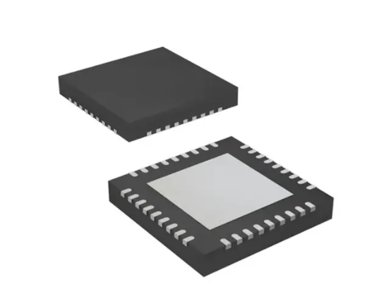
12 Package Outlines
Figure 17: RN6752V1 32-pin QFN Package Information
Rev. 1.6 – August.2020
Richnex Confidential and Proprietary
Page 41 of 41
�