Designated client product
This product will be discontinued its production in the near term.
And it is provided for customers currently in use only, with a time limit.
It can not be available for your new project. Please select other new or
existing products.
For more information, please contact our sales office in your region.
New Japan Radio Co.,Ltd.
www.njr.com
�NJM317
ADJUSTABLE 3-TERMINAL POSITIVE VOLTAGE REGULATOR
■ GENERAL DESCRIPTION
The NJM317 is adjustable 3-terminal positive voltage regulator IC.
It is capable of adjustment from typical 1.25V to 37V output voltage
range with two resistors. It is capable of supplying in excess of 1.5A
with heat sink.
The NJM317 is suitable for the power supply for general purpose.
■ FEATURES
Operating Voltage (+4.25V to +40V)
Adjustable Output Down to 1.2V
Guarantee'd 1.5A Output Current
Line Regulation typically (0.01%/V)
Load Regulation typically (0.1%)
80dB Ripple Rejection
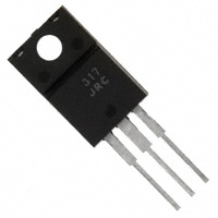
Package Outline TO-220F, TO-252
Bipolar Technology
■ PACKAGE OUTLINE
NJM317F
NJM317DL1
1. Adjustment
2. Output
3. Input
■ EQUIVALENT CIRCUIT
Ver.2016-04-20
-1-
�NJM317
■ ABSOLUTE MAXIMUM RATINGS
(Ta=25°C)
PARAMETER
Input-Output Differential Voltage
SYMBOL
RATINGS
UNIT
VIN - VO
40 (TC=25ºC)
V
PD
TO-220F 16 (TC≤70ºC)
TO-252 10 (Tc≤25ºC)
1 (Ta≤25ºC)
W
Topr (j)
Topr (a)
-40 to +150
-40 to +85
ºC
Tstg
-50 to +150
ºC
Power Dissipation
Operating Temperature Range (Junction)
(Ambient)
Storage Temperature Range
■ THERMAL CHARACTERISTICS
TO-220F
TO-252
Junction-To-Ambient
θja
60
125
Junction-To-Case
θjc
5
12.5
Thermal Resistance
ºC/W
■ ELECTRICAL CHARACTERISTICS (VIN - VO 5V, IO=500mA, CIN=0.1μF, CO1μF, Tj25ºC)
Measurement is to be conducted in pulse testing.
PARAMETER
Reference Voltage
SYMBOL
VREF
VREF-VIN
VREF-IO
Reference Voltage Thermal
Change
ΔVREF-T
Adjustment Pin Current
IADJ
TEST CONDITION
3V ≤ (VIN - VO) ≤ 40V, IO=100mA
10mA ≤ IO ≤ 1.5A (TO-220F)
10mA ≤ IO ≤ 500mA (TO-252)
0 ≤ Tj ≤ 125ºC
MIN.
TYP.
MAX.
UNIT
1.2
1.2
1.2
1.2
1.25
1.25
1.25
1.25
1.3
1.3
1.3
1.3
V
-
5
-
mV
-
50
100
μA
ΔIADJ - VIN
ΔIADJ - IO
3V ≤ (VIN - VO) ≤ 40V, IO=100mA
10mA ≤ IO ≤ 1.5A (TO-220F)
10mA ≤ IO ≤ 500mA (TO-252)
-
0.2
0.2
0.2
5
5
5
μA
ΔVO - VIN
3V ≤ (VIN - VO) ≤ 40V, IO=100mA
-
0.01
0.04
%/V
Load Regulation
ΔVO - IO
10mA ≤ IO ≤ 1.5A (TO-220F)
10mA ≤ IO ≤ 500mA (TO-252)
VO ≤ 5V
VO > 5V
-
5
0.1
25
0.5
mV
%
Minimum Load Current
IO(MIN)
(VIN - VO) = 40V
-
3.5
10
mA
Peak Output Current
IO(PEAK)
5V ≤ (VIN - VO) ≤ 15V
(VIN - VO) = 40V
1.5
0.15
2.2
0.4
-
A
RMS Output Noise Voltage
VNO
10Hz ≤ f ≤ 10kHz (RMS)
-
0.001
-
%/VO
Ripple Rejection Ratio
RR
VO 10V, f= 120Hz, ΔVIN =1Vrms
CADJ0
CADJ=10μF
66
65
80
-
Adjustment Pin Current
Change
Line Regulation
-2-
dB
Ver.2016-04-20
�NJM317
■ TEST CIRCUIT
1) (Reference Voltage Thermal Change), (Adjustment Pin Current Change), (Line Regulation), (Load Regulation),
(Peak Output Current), (RMS Output Noise Current)
2) Minimum Load Current
IOMIN: Minimum Io for
VO = VREF (Typical 1.25V)
(VIN = 40 + VREF)
3) Ripple Rejection
Ripple Rejection = 20log10 eIN [dB]
eo
Ver.2016-04-20
-3-
�NJM317
■ TYPICAL APPLICATIONS
1) VO = 1.25V to 37V Adjustable Voltage Regulator
VO = VREF x
R2
1
R1
+ R2 x IADJ
2) Selected Output Voltage
The transistors Q3 are switched by
selective signal inputs and the output
voltage VO is controlled by the transistor on
or off.
(Example)
When all transistor is off,
VO ·=· VREF x
R2
1
R1
When the transistor Q3 is on, and others
are off.
VO ·=· VREF x
R2 R3
1
(R
2
R3) R1
*IADJ ignore.
Selective Signal Inputs
3) Regulater with Protection Diodes
D1 protects about CO
D2 protects about CADJ
-4-
Ver.2016-04-20
�NJM317
4) Constant Current Regulator
R1 ≤ 125Ω
10mA ≤ IO ≤ 1.5A
IO =
VREF
R1
NJM317FA
NJM317DL1
Ver.2016-04-20
-5-
�NJM317
■ TYPICAL CHARACTERISTICS
Minimum Load Current
Peak Output Current
vs. Input-Output Differential Voltage
Output Voltage vs. Input Voltage.
Ripple Rejection vs. Frequency
Ripple Rejection vs. Output Voltage
-6-
Ripple Rejection vs. Output Current
Ver.2016-04-20
�NJM317
■ TYPICAL CHARACTERISTICS
Adjustment Pin Current vs. Temperature
Reference Voltage vs. Temperature
Load Regulation vs. Temperature
Line Regulation vs. Temperature
Thermal Shutdown
[CAUTION]
The specifications on this databook are only
given for information , without any guarantee
as regards either mistakes or omissions. The
application circuits in this databook are
described only to show representative usages
of the product and not intended for the
guarantee or permission of any right including
the industrial rights.
Ver.2016-04-20
-7-
�
很抱歉,暂时无法提供与“NJM317F”相匹配的价格&库存,您可以联系我们找货
免费人工找货