Designated client product
This product will be discontinued its production in the near term.
And it is provided for customers currently in use only, with a time limit.
It can not be available for your new project. Please select other new or
existing products.
For more information, please contact our sales office in your region.
New Japan Radio Co.,Ltd.
www.njr.com
�NJM4741
GENERAL PURPOSE QUAD OPERATIONAL AMPLIFIER
■ GENERAL DESCRIPTION
The NJM4741 consists of four independent high-gain
operational amplifiers that are designed for high slew rate, wide
band, and good noise characteristics.
■ FEATURES
● Operating Voltage
● Wide Band
● Slew Rate
● Low Input Noise Voltage
● Low Distortion
● Package Outline
● Bipolar Technology
( ±4V~±20V )
( 3.5MHz typ. )
( 1.6V/μs typ. )
( 9nV/√Hz typ. )
( 0.0005 typ. )
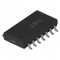
DIP14,DMP14
■ PACKAGE OUTLINE
NJM4741D
NJM4741M
■ PIN CONFIGURATION
NJM4741D
NJM4741M
PIN FUNCTION
1.A OUTPUT
2.A –INPUT
3.A +INPUT
+
4.V
5.B +INPUT
6.B –INPUT
7.B OUTPUT
8.C OUTPUT
9.C –INPUT
10.C +INPUT
11. V
12.D +INPUT
13.D –INPUT
14.D OUTPUT
■ EQUIVALENT CIRCUIT ( 1/4 Shown )
Ver.2017-10-23
-1-
�NJM4741
■ ABSOLUTE MAXIMUM RATINGS
( Ta=25˚C )
PARAMETER
Supply Voltage
Differential Input Voltage
Input Voltage
SYMBOL
+ V /V
VID
VIC
Power Dissipation
PD
Operating Temperature Range
Storage Temperature Range
Topr
Tstg
RATINGS
± 20
± 30
± 15 ( note )
( DIP14 ) 500
( DMP14 ) 300
-40~+85
-40~+125
UNIT
V
V
V
mW
˚C
˚C
( note ) When the supply voltage is less than ±15V,the absolute maximum input voltage is equal to the supply voltage.
■ ELECTRICAL CHARACTERISTICS
( Ta=25˚C,V+/V-=±15V )
PARAMETER
Input Offset Voltage
Input Offset Current
Input Bias Current
Large Signal Voltage Gain
Operating Current
Common Mode Rejection Ratio
Supply Voltage Rejection Ratio
Maximum Output Voltage 1
Maximum Output Voltage 2
Input Common Mode Voltage Range
Slew Rate
Equivalent Input Noise Voltage
Channel Separation
SYMBOL
VIO
IIO
IB
AV
ICC
CMR
SVR
VOM1
VOM2
VICM
SR
en
CS
TEST CONDITION
RS≤100Ω
RL≥2kΩ,VO=±10V
RL≥10kΩ
RL≥2kΩ
Av=1
f=1kHz
f=10kHz,Input Referred
MIN.
88
80
80
± 12
± 10
± 12
-
TYP.
1.0
5
60
110
5
120
120
± 13.7
± 12.5
± 14
1.6
9
108
MAX.
5.0
50
300
7
-
UNIT
mV
nA
nA
dB
mA
dB
dB
V
V
V
V/μs
nV/√Hz
dB
( note ) The application that leads to the extreme difference of power dissipation between channels may cause the mutual interference by the temperature gradient
on the chip.
-2-
Ver.2017-10-23
�NJM4741
■ TYPICAL CHARACTERISTICS
Ver.2017-10-23
-3-
�NJM4741
■ TYPICAL CHARACTERISTICS
-4-
Ver.2017-10-23
�NJM4741
■ TYPICAL CHARACTERISTICS
[CAUTION]
The specifications on this databook are only
given for information , without any guarantee
as regards either mistakes or omissions. The
application circuits in this databook are
described only to show representative usages
of the product and not intended for the
guarantee or permission of any right including
the industrial rights.
Ver.2017-10-23
-5-
�
很抱歉,暂时无法提供与“NJM4741M”相匹配的价格&库存,您可以联系我们找货
免费人工找货