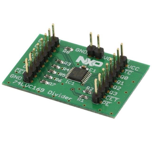
NXP 74LVC169
demo board
Demonstrate a binary counter for
high-speed counting applications
This compact demo board makes it easy to evaluate the 74LVC169, a binary counter with internal
look-ahead carry circuitry for cascading in high-speed counting applications.
Key features and benefits
} 5 V tolerant inputs for interfacing with 5 V logic and use in
3/5 V mixed voltage applications
} Wide supply voltage range: 1.2 to 3.6 V
} CMOS low power consumption for portable applications
} Direct interface with TTL levels
} Up/down counting
} Two count enable inputs for n-bit cascading
} Built-in look-ahead carry capability
} Presettable for programmable operation
} Multiple extremely small standard and leadless packages
} Wide operating temperature range (-40 to +125 °C), suitable
for industrial and automotive applications
Applications
} Portable devices
} Industrial
} Automotive
The 74LVC169 is a synchronous presettable 4-bit binary
counter which features an internal look-ahead carry circuitry
for cascading in high-speed counting applications.
Synchronous operation is provided by having all flip-flops
clocked simultaneously so that the outputs (pins Q0 to Q3)
change simultaneously with each other when instructed by the
count-enable (pins CEP and CET) inputs and internal gating.
This mode of operation eliminates the output counting spikes
that are normally associated with asynchronous (ripple clock)
counters. A buffered clock (pin CP) input triggers the four flipflops on the LOW-to-HIGH transition of the clock.
The counter is fully programmable; that is, the outputs may
be preset to any number between 0 and its maximum count
of 15. Presetting is synchronous with the clock and takes place
regardless of the levels of the count enable inputs. A LOW
level on the parallel enable (pin PE) input disables the counter
and causes the data at the Dn input to be loaded into the
counter on the next LOW-to-HIGH transition of the clock.
The direction of the counting is controlled by the up/down
(pin U/D) input. When pin U/D is HIGH, the counter counts up,
when LOW, it counts down.
�The look-ahead carry circuitry is provided for cascading
counters for n-bit synchronous applications without additional
gating. Instrumental in accomplishing this function are two
count-enable (pins CEP and CET) inputs and a terminal
count (pin TC) output. Both count-enable (pins CEP and CET)
inputs must be LOW to count. Input pin CET is fed forward
to enable the terminal count (pin TC) output. Pin TC thus
enabled will produce a LOW-level output pulse with a duration
approximately equal to a HIGH level portion of pin Q0 output.
The LOW level pin TC pulse is used to enable successive
cascaded stages.
The main clock, when connected to the CP pin, is divided by
2 and appears at the Q0 output. There is a clock with 1/4 the
frequency of the main clock at Q1. Clocks with 1/8 and 1/16
of main frequency are available at Q2 and Q3 output pins
respectively.
In order to preset the outputs of the counter to a number
between 0 and its maximum count, the PE pin can be pulled
LOW by using jumper JP1. Data at Dn inputs can now be
loaded to the outputs on next LOW-to-HIGH transition of
main clock. Also, U/D pin can be pulled HIGH by providing
logic high input at pin 1 of P1 connector to count up instead
of counting down. Since CET pin is pulled LOW, when counter
reaches terminal count (HHHH in count up mode and LLLL in
count down mode), TC output, which is normally HIGH, will
go LOW. The low level on TC output can be used to enable
successive cascaded devices
Schematics of 74LVC169 demo board are shown in figure
below. A supply voltage of 1.2 to 3.6 V can be used for the
board. In this design, the 74LVC169 is used as a clock divider
that divides the main clock connected to CP pin by 2, 4, 8
and 16. By default, U/D pin is pulled low and PE pin is pulled
HIGH, so counter starts counting down, when clock input edge
goes from LOW to HIGH.
VCC
2
1
C1
JP1
0.1uF
GND
P1
IC1
VCC
TC
Q0
Q1
Q2
Q3
CET
PE
4.7k
74LVC169PW
GND
R2
R7 4.7k
R6 4.7k
R5 4.7k
R4 4.7k
R3 4.7k
GND
P2
1
2
3
4
5
6
7
8
U/D VCC
TC
CP
Q0
D0
Q1
D1
Q2
D2
Q3
D3
CEP CET
GND PE
CLK
D0
D1
D2
D3
CEP
R8 4.7k
1
2
3
4
5
6
7
8
R1
GND
GND
GND
Circuit schematic of 74LVC169 demo board
NXP SEMICONDU
TITLE: 74LVC169 Evaluation Boar
Document Number:
�Test results
Figure 1 shows a main clock of 466 kHz in green at CP input
and a divided-by-2 clock output of 233 kHz in purple at Q0
pin. By default PE pin is pulled up to VCC and U/D pin is pulled
down to GND. Figure 2 shows a main clock of 500 kHz in green
at CP input. The Q1 output shows a divided-by-4 clock of
approximately 166 kHz in purple. In this case, U/D pin is pulled
up so counter starts counting up on rising edge of input clock.
Similarly, Figures 3 and 4 show the clock outputs of 71 and
33 kHz, which are approximately 1/8 and 1/16 of main clock
respectively. Since U/D is pulled LOW for clock output in these
examples, counter is counting down.
Figure 1
Figure 2
Figure 3
Figure 4
�Packages
74LVC169 is available in 16-pin SO, SSOP, TSSOP and leadless DQFN packages.
Package suffix
D
PW
BQ
DS
SOT109-1
SOT403-1
SOT763-1
SOT338-1
16-pin
16-pin
16-pin
16-pin
Width (mm)
6.0
6.4
2.5
7.75
Length (mm)
9.9
5.0
3.5
6.2
Pitch (mm)
1.27
0.65
0.5
0.65
Ordering information
Part number
Package
Temp. range
Name
Type
Marking
Material
74LVC169
-40 to 125 °C
SO16
Small outline
74LVC169D
Plastic
74LVC169DB
-40 to 125 °C
SSOP16
Shrink small outline
LVC169
Plastic
74LVC169PW
-40 to 125 °C
TSSOP16
Thin shrink small outline
LVC169
Plastic
74LVC169BQ
-40 to 125 °C
DHVQFN16
Dual in-line compatible thermal enhanced
very thin quad flat package with no leads
LVC169
Plastic
www.nxp.com
© 2010 NXP B.V.
All rights reserved. Reproduction in whole or in part is prohibited without the prior written consent of the copyright owner.
Date of release: March 2010
The information presented in this document does not form part of any quotation or contract, is believed to be accurate and
Document order number: 9397 750 16884
reliable and may be changed without notice. No liability will be accepted by the publisher for any consequence of its use.
Printed in the Netherlands
Publication thereof does not convey nor imply any license under patent- or other industrial or intellectual property rights.
�
很抱歉,暂时无法提供与“OM13336,598”相匹配的价格&库存,您可以联系我们找货
免费人工找货- 国内价格
- 1+1178.94960
- 200+470.41560
- 500+454.69080
- 1000+446.92560