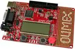
STM32-P152 development board
user's manual
All boards produced by Olimex are ROHS compliant
Revision C, April 2012
Copyright(c) 2011, OLIMEX Ltd, All rights reserved
Page 1
�INTRODUCTION:
STM32-P152 is a development board with STM32L152VBT6 ARM Cortex M3 microcontroller made by STMicroelectronics. This microcontroller supports various
communication interfaces such as USB, three USARTs, two SPIs, two I2Cs. There are
USB, JTAG and UEXT connectors, three buttons – WKUP, USER and RESET, four
status LEDs, potentiometer and pin holes for most of the microcontroller's pins. The
board features low power segment LCD that uses the built in LCD controller in this
specialized microcontroller. Due to its low power capabilities the board can run battery powered applications via the battery connector. All this allows you to build different projects for a wide range of applications.
BOARD FEATURES:
MCU: STM32L152VBT6 – 128 KB Flash, 16 KB Data RAM
USB
3.7V-LI_BAT connector
Battery charger
JTAG/SWD connector
UEXT connector
RS232 connector
LCD
Four status LEDs
Reset circuit
RESET button
WKUP button
USER button
Potentiometer
Power jack
Power-on LED
Pin holes for most of the microcontroller pins
FR-4, 1.5 mm, soldermask, component print
Dimensions: 120.00 x 80.00 mm (4.72 x 3.15")
Page 2
�ELECTROSTATIC WARNING:
The STM32-P152 board is shipped in protective anti-static packaging. The board
must not be subject to high electrostatic potentials. General practice for working
with static sensitive devices should be applied when working with this board.
BOARD USE REQUIREMENTS:
Cables: The cable you will need depends on the programmer/debugger you use. If
you use ARM-JTAG-EW, ARM-USB-TINY or ARM-USB-TINY-H, you will need
USB A-B cable, if you use ARM-USB-OCD or ARM-USB-OCD-H, you will need
USB A-B cable and RS232 cable.
Hardware: Programmer/Debugger ARM-USB-OCD, ARM-USB-OCD-H, ARMUSB-TINY, ARM-USB-TINY-H, ARM-JTAG-COOCOX or other compatible
programming/debugging tool if you work with EW-ARM. It is a good practice to
first consider the software tools you are going to use and check if they support the
debuggers.
It is good idea to use SWD interface for debugging/programming because of the
multiplexing of the JTAG signal lines with the display lines. If using a debugger
that supports only JTAG layout you might need to disable display or write a
routine that disables it.
PROCESSOR FEATURES:
STM32-P152 board uses ARM 32-bit Cortex™-M3 microcontroller
STM32L152VBT6 from STMicroelectronics has these features:
Operating conditions
Operating power supply range: 1.65 V to 3.6 V (without BOR) or 1.8 V to
3.6 V (with BOR option)
Temperature range: –40 to 85 °C
Low power features
4 modes: Sleep, Low-power run (9 μA at 32 kHz), Low-power sleep (4.4
μA), Stop with RTC (1.45 μA), Stop (570 nA), Standby (300 nA)
Dynamic core voltage scaling down to 233 μA/MHz
Ultra low leakage per I/O: 50 nA
Fast wakeup from Stop: 8 μs
Three wakeup pins
Core: ARM 32-bit Cortex™-M3 CPU
32 MHz maximum frequency, 33.3 DMIPS peak (Dhrystone 2.1)
Page 3
�
Reset and supply management
Low power, ultrasafe BOR (brownout reset) with 5 selectable thresholds
Ultralow power POR/PDR
Programmable voltage detector (PVD)
Clock management
1 to 24 MHz crystal oscillator
32 kHz oscillator for RTC with calibration
Internal 16 MHz factory-trimmed RC
Internal 37 kHz low consumption RC
Internal multispeed low power RC, 64 kHz to 4 MHz with a consumption
down to 1.5 μA
PLL for CPU clock and USB (48 MHz)
Low power calendar RTC
Memory protection unit
Alarm, periodic wakeup from Stop/Standby
Memories
128 Kbyte of Flash memory with ECC
4 Kbyte of data EEPROM with ECC
16 Kbyte of RAM
83 fast I/Os (73 of which are 5 V-tolerant) all mappable on 16 external interrupt
vectors
Development support
Serial wire debug, JTAG and trace
DMA: 7-channel DMA controller, supporting timers, ADC, SPIs, I2Cs and
USARTs
LCD 8 × 40 or 4 × 44 with step-up converter
12-bit ADC up to 1 Msps/24 channels
Temperature sensor and internal voltage reference
Operates down to 1.8 V
2× 12-bit DACs with output buffers
2 ultralow power comparators
Window mode and wakeup capability
10 timers:
6 × 16-bit general-purpose timers, each with up to 4 IC/OC/PWM channels
2 × 16-bit basic timers
Page 4
�
2 × watchdog timers (independent and window)
8 communication interfaces:
2 × I2C interfaces (SMBus/PMBus)
3 × USARTs (ISO 7816 interface, LIN, IrDA capability, modem control)
2 × SPIs (16 Mbit/s)
USB 2.0 full speed interface
CRC calculation unit, 96-bit unique ID
Page 5
�BLOCK DIAGRAM:
AF = Alternate Function function on I/O port pin.
Page 6
�MEMORY MAP:
Page 7
�Page 8
1
1uF/10V
SEG36
SEG37
T 11 03NE-12x1 2x4.3
3 .3V
RS232_EN
T1
47k
12
9
11
10
5
DTA11 4YKA
330R
33 0R
SEG34
SEG35
USART2 _RX
R2 6
USART2_CTS R43
USART2_TX
USART2_RTS
3
C26
4
100n F
C27
1
10 0nF
GND15
U4PWR
C30
100n F
16VCC
R1IN
R2IN
T1OUT
T2OUT
V-
V+
CTS
RTS
6
7
8
9
NC
RS2 32_2
1
2
3
4
5
C1
100n F
C25
100nF
R14
g
a
d
RS232 DRIVERS
13
8
14
7
6
2
ST3232 CDR(SO 16)
R1OUT
R2OUT
T1IN
T2IN
C2-
C2+
C1-
C1+
U4
OLIMEX
e
24
100nF
umHF
SEG32
SEG33
C28
48
2
RESET
COM2
COM3
3
R40
100k
4
46
C31
100 nF
45
COM0
COM1
SEG30
SEG31
330R
R11
100R/1%
5
GND
6
44
W KUP
43
TRACED0/SEG39
TRACECK/SEG38
SEG28
SEG29
R39
7
330R
42
33 0R
SEG0
SEG1
SEG26
SEG27
R13
1 00R/1%
RST
8
R44
9
41
SEG16
TDI/SEG17
R12
100R/1 %
40
SEG24
SEG25
3.3V
10
R8
1 0k
11
39
SEG14
SEG15
NA (S TM1001R W X 6F)
2 VCC RESET 1
12
38
U2
37
SEG22
SEG23
C24
100n F
13
SEG20
SEG21
W KUP
OLIMEX_LTD
LCD
AG ND
14
36
SEG18
SEG19
USER
2
35
SEG3
SEG2
SEG42
f
15
SENSE_E
BAT
1
CLO SE
G NDA_E
C1 0
1uF/10 V
34
18
RESET CIRCUIT
C33
100 nF
DW 02R
G ND
GND
3
SEG10
SEG11
19
R41
R52
10k
-
VIN
VOUT
3.3V
16
20
C35
2.2u F/6.3 V
R9
33 k
1
2
BAT
3.7 V-L I_BAT
1
2
MCP1702T-3302E/MB
VR(3 .3V)
17
33
21
USER
R42
10k
2.2uF/6.3V
appr. 70 mA charge current
15 k
VSSPROG
5
1
3
D1
BAT54C
32
22
3.3V
VDDVBAT
BATTERY CE
CHARGER
+
R51
2
4
R53
4.7k
FET1
IRLML6402
470R
TRST/SEG8
SEG9
23
BUTTONS
C34
U5
MCP73812T-420I/OT
+5V
Battery Charger
+5V
R45
PW R_LED
RED(G YX-SD-TC080 5SYRK)
C14 10pF
C15 10p F
GND
30
47
BZV55 C6 V2
C4
VIN
3.3V
PC10
PC11
Q2
NA
32768 Hz/6 pF
RS232_ EN
TRIMER_ EN
SEG 43
USART2_CTS
USART2_RTS
USART2 _TX
USART2_RX
SENSE_E
PD7
SEG 2 8
SEG 29
SEG 30
SEG 3 1
SEG 32
SEG 33
SEG 34
SEG 35
R33
SEG 1 8
SEG 19
SEG 20
SEG 2 1
SEG 22
SEG 23
SEG 24
SEG 2 5
SEG 26
SEG 27
USART3_TX
USART3 _RX
SEG 42
USER
TMS/SWDIO
TCK/SWCLK
SEG6
TDO/TRACESWO/SEG7
31
Z2
D4
BAT54C
D2
BAT54 C
PWR_L ED_E
HN1x2
81
82
83
84
85
86
87
88
55
56
57
58
59
60
61
62
SEG [0..6],SEG [9 ..16],SEG [18..37 ],SEG 42,SEG 43 ,CO M[0..3]
OSC_IN/PD0/SPI2_NSS/TIM9_CH1
OSC_OUT/PD1/SPI2_SCK
PD2/TIM3_ETR/LCD_SEG31/LCD_SEG43/LCD_COM7
PD3/USART2_CTS/SPI2_MISO
PD4/USART2_RTS/SPI2_MOSI
PD5/USART2_TX
PD6/USART2_RX
PD7/USART2_CK/TIM9_CH2
PD8/USART3_TX/LCD_SEG28
PD9/USART3_RX/LCD_SEG29
PD10/USART3_CK/LCD_SEG30
PD11/USART3_CTS/LCD_SEG31
PD12/TIM4_CH1/USART3_RTS/LCD_SEG32
PD13/TIM4_CH2/LCD_SEG33
PD14/TIM4_CH3/LCD_SEG34
PD15/TIM4_CH4/LCD_SEG35
15
16
17
18
33
34
63
64
65
66
78
79
80
7
8
9
PB2
DAC_O UT1
DAC_ O UT2
SEG 5
SEG 6
PB2 /BO O T1
TDO /TRACESW O /SEG 7
TRST/SEG 8
SEG 9
PB6
I2 C1 _SCL
PB7
I2C1_SDA
SEG 16
CO M3
SEG 10
SEG 1 1
SEG 12
SEG 13
SEG 1 4
SEG 15
W KUP
SEG 0
SEG 1
SEG 2
DAC_O UT1
DAC_O UT2
SEG 3
SEG 4
CO M0
CO M1
CO M2
USB_ DM
USB_DP
TMS/SWDIO
TCK/SWCLK
TDI/SEG 17
28
3.3V
STM32L 152VBT6
PE0/TIM4_ETR/LCD_SEG36/TIM10_CH1
PE1/LCD_SEG37/TIM11_CH1
PE2/TRACECK/LCD_SEG38/TIM3_ETR
PE3/TRACED0/LCD_SEG39/TIM3_CH1
PE4/TRACED1/TIM3_CH2
PE5/TRACED2/TIM9_CH1
PE6/TRACED3/WKUP3/TIM9_CH2
PE7/ADC_IN22/COMP1_INP
PE8/ADC_IN23/COMP1_INP
PE9/ADC_IN24/TIM2_CH1_ETR/COMP1_INP
PE10/ADC_IN25/TIM2_CH2/COMP1_INP
PE11/TIM2_CH3
PE12/TIM2_CH4/SPI1_NSS
PE13/SPI1_SCK
PE14/SPI1_MISO
PE15/SPI1_MOSI
NRST
PH2/I2C2_SMBA
OSC_OUT/PH1
OSC_IN/PH0
PC0/ADC_IN10/LCD_SEG18/COMP1_INP
PC1/ADC_IN11/LCD_SEG19/COMP1_INP
PC2/ADC_IN12/LCD_SEG20/COMP1_INP
PC3/ADC_IN13/LCD_SEG21/COMP1_INP
PC4/ADC_IN14/LCD_SEG22/COMP1_INP
PC5/ADC_IN15/LCD_SEG23/COMP1_INP
PC6/TIM3_CH1/LCD_SEG24
PC7/TIM3_CH2/LCD_SEG25
PC8/TIM3_CH3/LCD_SEG26
PC9/TIM3_CH4/LCD_SEG27
PC10/USART3_TX/LCD_SEG28/LCD_SEG40/LCD_COM4
PC11/USART3_RX/LCD_SEG29/LCD_SEG41/LCD_COM5
PC12/USART3_CK/LCD_SEG30/LCD_SEG42/LCD_COM6
PC13/RTC_AF1/WKUP2
PC14/OSC32_IN
PC15/OSC32_OUT
35
36
37
89
90
91
92
93
95
96
47
48
51
52
53
54
23
24
25
26
29
30
31
32
67
68
69
70
71
72
76
77
26
SEG4
SEG5
29
G ND_ PIN
97
98
1
2
3
4
5
38
39
40
41
42
43
44
45
46
SEG 36
SEG 3 7
TRACECK/SEG 38
TRACED0/SEG 39
TRACED1
TRACED2
TRACED3
TRIM
BAT
STAT3
STAT4
SPI1 _NSS
SPI1_SCK
SPI1_MISO
SPI1 _MO SI
14
73
RST
+5V_ USB R7
4.7k
13
12
BOOT0
VLCD
PB0/ADC_IN8/TIM3_CH3/LCD_SEG5/COMP1_INP/VREF_OUT
PB1/ADC_IN9/TIM3_CH4/LCD_SEG6/COMP1_INP/VREF_OUT
PB2/BOOT1
JTDO/TIM2_CH2/PB3/TRACESWO/SPI1_SCK/COMP2_INM/LCD_SEG7
JNTRST/TIM3_CH1/PB4/SPI1_MISO/COMP2_INP/LCD_SEG8
PB5/I2C1_SMBAL/TIM3_CH2/SPI1_MOSI/COMP2_INP/LCD_SEG9
PB6/I2C1_SCL/TIM4_CH1/USART1_TX/LCD_SEG8
PB7/I2C1_SDA/TIM4_CH2/USART1_RX/PVD_IN
PB8/TIM4_CH3/I2C1_SCL/LCD_SEG16/TIM10_CH1
PB9/TIM4_CH4/I2C1_SDA/LCD_COM3/TIM11_CH1
PB10/I2C2_SCL/USART3_TX/TIM2_CH3/LCD_SEG10
PB11/I2C2_SDA/USART3_RX/TIM2_CH4/LCD_SEG11
PB12/SPI2_NSS/I2C2_SMBA/USART3_CK/LCD_SEG12/ADC_IN18/COMP1_INP/TIM10_CH1
PB13/SPI2_SCK/USART3_CTS/LCD_SEG13/ADC_IN19/COMP1_INP/TIM9_CH1
PB14/SPI2_MISO/USART3_RTS/LCD_SEG14/ADC_IN20/COMP1_INP/TIM9_CH2
PB15/SPI2_MOSI/TIM1_CH3N/LCD_SEG15/ADC_IN21/COMP1_INP/TIM11_CH1/RTC_50_60HZ
PA0/WKUP1/USART2_CTS/ADC_IN0/TIM2_CH1_ETR/COMP1_INP
PA1/USART2_RTS/ADC_IN1/TIM2_CH2/LCD_SEG0/COMP1_INP
PA2/USART2_TX/ADC_IN2/TIM2_CH3/TIM9_CH1/LCD_SEG1/COMP1_INP
PA3/USART2_RX/ADC_IN3/TIM2_CH4/TIM9_CH2/LCD_SEG2/COMP1_INP
PA4/SPI1_NSS/USART2_CK/ADC_IN4/DAC_OUT1/COMP1_INP
PA5/SPI1_SCK/ADC_IN5/DAC_OUT2/TIM2_CH1_ETR/COMP1_INP
PA6/SPI1_MISO/ADC_IN6/TIM3_CH1/TIM1_BKIN/LCD_SEG3/TIM10_CH1/COMP1_INP
PA7/SPI1_MOSI/ADC_IN7/TIM3_CH2/TIM1_CH1N/LCD_SEG4/TIM11_CH1/COMP1_INP
PA8/USART1_CK/MCO/LCD_COM0
PA9/USART1_TX/LCD_COM1
PA10/USART1_RX/LCD_COM2
PA11/USART1_CTS/USBDM/SPI1_MISO
PA12/USART1_RTS/USBDP/SPI1_MOSI
JTMS/SWDIO/PA13
JTCK/SWCLK/PA14
JTDI/TIM2_CH1_ETR/PA15/SPI1_NSS/LCD_SEG17
SEG13
SEG12
27
+5V_JTAG
+5V_JTAG
EXT_PWR
6
94
VREF-
VREF+
VSSA
VDDA
VSS_5
VSS_4
VSS_3
VSS_2
VSS_1
2
1
+5V_ USB
Q1
B0_1 /B0_ 0
10 k
R15
20
21
U1
VDD_1
VDD_2
VDD_3
VDD_4
VDD_5
SEG43
+5V_USB
+5V_J-TRACE
PE8
PE9
PE1 0
PE11
PE12
PE1 3
PE14
PE15
RST
VREF-
NA
1 00nF
19
22
10
27
99
74
49
50
75
100
28
11
POWER SUPPLY CIRCUIT
C13
27pF
C9
10 0nF
VREF+
C20
1u F/10V
HN1x3
0
C21
C29
Q8.000MHz/HC-49SM(SMD)/20pF
C12
27pF
0 R(NA)
3.3 V
0R
0R
0 R(NA)
3.3V_A
C11 1uF/10 V
C19
1u F/10V
3.3V_A
3 .3V
25
YDJ-1136
5 -6VDC
6VDC MAX!!!
PW R
1
2
3
+5V_JTRACE
R5
R20
R50 PB2/BO O T1
1
1
2
3
B1_ 1/B1 _0
HN1x3
2
FB0805/600R/200mA(201209-601)
C23 100nF
10k
C8 4.7uF
0
C7 100nF
FB1
CLO SE
1
SHUNT_E
2
C6 100nF
3.3 V
1R
R6
C5 100nF
CLO SE
2
1
USB_DP,USB_DM
c
b
SPI1 _MO SI
SPI1_MISO
SPI1_ SCK
SPI1 _NSS
USART3_TX
USART3_RX
I2C1_SCL
I2 C1 _SDA
TMS/SWDIO ,TCK/SW CLK
R2
R1
100 k
VIN
UEXT
R49
270R
T2
BC817-40
100n F
C32
1
3
5
7
9
0R
0R
1
2
3
(NA)USBL C6 -2P6
6
5
4
R4
100 k
270R
R3
3 .3V
R32
4.7k
DAC_O UT2
10k
10k
BZV55C6V2
+5V_JTAG
2
4
6
8
10
12
14
16
18
20
1
3
5
7
9
11
13
15
17
19
1
3
5
7
9
11
13
15
17
19
TRACE
BH20S
2
4
6
8
10
12
14
16
18
20
JTAG /SWD
C3
10 0nF
3 .3V
3 30R
R24
3 .3V
R47
4 70R
STAT3
RED(GYX-SD-TC0805SYRK)
STAT3
R46
4 70R
C18
100nF
TRIM
10nF(NA)
C2
STAT4
SPI1_SCK,SPI1_MOSI,SPI1_MISO,SPI1_NSS,I2C1_SDA,I2C1_SCL,USART3_RX,USART3_TX
1 0k
T1107A(6x3,8x2,5mm)
3
T1103NE-12x12x4.3
http ://www.o limex.co m/dev
STAT4
GREEN(GYX-SD-TC0805SGC)
CO PYRIG HT(C) 2011, O LIMEX Ltd .
Rev. B
STM32-P152
R48
270R
T3
BC817-40
YELLOW(GYX-SD-TC0805SYC)
STAT2
1 0k(NA)
R10
STATUS LEDS
TRIMER_EN
AN_TR
10 k
3.3V
S HIE L D
R38
1M
1
2
3
4
USB
USB_B
+5V_J-TRACE
3 .3V
3.3V
C22
10 0nF
+5V_ USB
TRIMMER
G PH127 -SMT02x10 (pin7-CUT)/(NA)
TRACED2
TRACED3
10k
R18
R17
R16
NA
R23
R25
NA
0R(NA)
NA
0 R(NA)
NA
NA
R29
NA
USART3 _TX
I2C1_ SCL
SPI1_MISO
SPI1_SCK
3 .3V
R37
R36
R35
R3 4
R27
R28
NA
GREEN(GYX-SD-TC0805SGC)
STAT1
BH10S
2
4
6
8
10
UEXT
USART3 _RX
I2C1_ SDA
SPI1_MO SI
SPI1_NSS
270R
R3 1
4.7k
DAC_O UT1
R3 0
33k
O PEN
TMS/SWDIO
TCK/SWCLK
TDO /TRACESW O /SEG 7
TDI/SEG 1 7
RST
TRACECK/SEG 38
TRACED0/SEG 39
TDO /TRACESWO /SEG 7
TRACED1
TRST/SEG 8
3 .3V
R19
NA
R22
R21
U3
Z1
JTAG/SWD/TRACE
47pF(NA)
TDO /TRACESWO /SEG 7
RST
R-T
TRST/SEG 8
1
2
TRST/SEG 8
TDI/SEG 17
TMS/SWDIO
TCK/SWCLK
47pF(NA)
22 R
C17
USB_ DM
C16
22R
USB_DP
3 .3V
USB CIRCUIT
USB
3.3VA_MCU_E
3.3V_ MCU_E
HN1x2
SCHEMATIC:
�BOARD LAYOUT:
POWER SUPPLY CIRCUIT:
STM32-P152 can take power from:
–PWR_JACK (5-6) VDC
–USB - +5V_USB.
–JTAG - +5V_JTAG.
–TRACE - +5V_J-TRACE
–Battery connector – +3.7V lithium battery.
–Pin Hole VIN – (5÷6) VDC.
The programmed board power consumption is about 50 mA with all peripherals
enabled. The minimal current consumption is a few uA(up to 10)
Note that if the battery is connected to 3,7V-Li BAT connector and some of other
power sources(USB, JTAG, TRACE, PWR_JACK) are present and the battery is
discharged then the battery will be charge until the charge complete.
RESET CIRCUIT:
STM32-P152 reset circuit includes R8 (10k), R44 (330Ω), R11 (100Ω/1%), C28
(100nF), STM32L152VBT6 pin 14 (NRST) and RESET button.
Page 9
�CLOCK CIRCUIT:
Quartz crystal (Q1) 8 MHz is connected to STM32L152VBT6 pin 12 (OSC_IN/PH0)
and pin 13 (OSC_OUT/PH1).
Quartz crystal (Q2) 32.768 kHz is connected to STM32L152VBT6 pin 8
(PC14/OSC32_IN) and pin 9 (PC15/OSC32_OUT).
JUMPER DESCRIPTION:
R-T
When this jumper is closed, RST and TRST/SEG8 are connected. When this jumper is
opened, RST and TRST/SEG8 are separated.
Default state is opened.
SHUNT_E
When this jumper is closed, 1 Ohm shunt is enabled. When this jumper is opened, 1
Ohm shunt is disabled.
Default state is closed.
GNDA_E
When this jumper is closed, the board analog ground is enabled. When this jumper is
opened, the board analog ground is disabled.
Default state is closed.
3.3VA_MCU_E
When this jumper is closed, the microcontroller analog power is enabled. When this
jumper is opened, the microcontroller analog power is not enabled.
Default state is closed.
3.3V_MCU_E
When this jumper is closed, STM32L152VBT6 power supply is enabled. When this
jumper is opened, STM32L152VBT6 power supply is disabled.
Default state is closed.
PWR_LED_E
When this jumper is closed, the PWR_LED is enabled. When this jumper is opened,
the PWR_LED is disabled.
Default state is closed.
B0_1/B0_0
This jumper, when is in position B0_1 – connects STM32L152VBT6 pin 94 (BOOT0) via
R15 (10k) to 3.3V, when the jumper is in position B0_0 – connects STM32L152VBT6
pin 94 (BOOT0) via R15 (10k) to GND.
Default state is closed in position B0_0.
Page 10
�B1_1/B1_0
This jumper, when is in position B1_1 – connects STM32L152VBT6 pin 37
(PB2/BOOT1) via R7 (10k) to 3.3V, when the jumper is in position B1_0 – connects
STM32L152VBT6 pin 37 (PB2/BOOT1) via R7 (10k) to GND.
Default state is closed in position B1_0.
The boot mode is selected depending on jumpers B0_1/B0_0 and B1_1/B1_0
configuration:
- When B0_1/B0_0 is closed in position B0_0 and B1_1/B1_0 position doesn't matter the boot mode is Main Flash Memory.
- When B0_1/B0_0 is closed in position B0_1 and B1_1/B1_0 is closed in position B1_0
– the boot mode is System Memory.
- When B0_1/B0_0 is closed in position B0_1 and B1_1/B1_0 is closed in position B1_1
– the boot mode is Embedded SRAM.
INPUT/OUTPUT:
Status led (green), with name STAT1 is connected to STM32L152VBT6 pin 29
(PA4/DAC_OUT1), allowing current through it to be adjusted smoothly.
Status led (yellow), with name STAT2 is connected to STM32L152VBT6 pin 30
(PA5/DAC_OUT2), allowing current through it to be adjusted smoothly.
Status led (red), with name STAT3 is connected to STM32L152VBT6 pin 41 (PE10).
Status led (green), with name STAT4 is connected to STM32L152VBT6 pin 42
(PE11).
Power-on led, with name PWR_LED – this led shows that the board is power
supplied.
User button with name WKUP is connected to STM32L152VBT6 pin 23
(PA0/WKUP1).
User button with name USER is connected to STM32L152VBT6 pin 7
(PC13/WKUP2).
User button with name RESET is connected to STM32L152VBT6 pin 14 (NRST).
Trimmer with name AN_TR is connected to STM32L152VBT6 pin 82
(PD1/SPI2_SCK) – signal “TRIMER_EN”.
Page 11
�EXTERNAL CONNECTORS DESCRIPTION:
UEXT:
Pin #
Signal Name
1
VCC (3.3V)
2
GND
3
USART3_TX
4
USART3_RX
5
I2C1_SCL
6
I2C1_SDA
7
SPI1_MISO
8
SPI1_MOSI
9
SPI1_SCK
10
SPI1_NSS
USB:
Pin #
Signal Name
1
+5V_USB
2
USB_DM
3
USB_DP
4
GND
3.7V-LI_BAT:
Pin #
Signal Name
1
VBAT
2
GND
Page 12
�JTAG/SWD:
Pin #
Signal Name
Pin #
Signal Name
1
VCC (3.3V)
2
VCC (3.3V)
3
TRST/SEG8
4
GND
5
TDI/SEG17
6
GND
7
TMS/SWDIO
8
GND
9
TCK/SWCLK
10
GND
11
Via 10k to GND
12
GND
13
TDO/TRACESWO/SEG7
14
GND
15
RST
16
GND
17
Via 10k to GND
18
GND
19
+5V_JTAG
20
GND
Important: The default demo software blocks the JTAG communication. A workaround is to
press and hold button B2, then press RST, then release B2. This will shut down the display
allowing you to erase the demo via JTAG and after that the JTAG should be available.
SWD debuggers/programmers would not have such a problem.
Page 13
�PWR_JACK:
Pin #
Signal Name
1
EXT_PWR
2
GND
RS232_2:
Pin #
Signal Name
1
Not Connected
2
T1OUT (U4 pin 14)
3
R1IN (U4 pin 13)
4
Not Connected
5
GND
6
Not Connected
7
CTS
8
RTS
9
Not Connected
TRACE:
Pin #
Signal Name
Pin #
Signal Name
1
VCC (3.3V)
2
TMS/SWDIO
3
GND
4
TCK/SWCLK
5
GND
6
TDO/TRACESWO/SEG7
7
Not Connected
8
TDI/SEG17
9
GND
10
RST
Page 14
�11
+5V_J-TRACE
12
TRACECK/SEG38
13
+5V_J-TRACE
14
TRACED0/SEG39
15
GND
16
TRACED1
17
GND
18
TRACED2
19
GND
20
TRACED3
Page 15
�PIN HOLES:
Page 16
�MECHANICAL DIMENSIONS:
Page 17
�AVAILABLE DEMO SOFTWARE:
Demo software USB mouse and Blinking LED for EW-ARM
Setup GCC+Eclispse for STM32 on MAC
Page 18
�ORDER CODE:
STM32-P152 - assembled and tested board
How to order?
You can order to us directly or by any of our distributors.
Check our web https://www.olimex.com/ or more info.
Revision history:
Board's revision:
Rev. B, June 2011
Manual's revision:
Rev. Initial, September 2011
Manual's revision:
Rev. B, March 2013
Manual's revision:
Rev. C, April 2013
Page 19
�Disclaimer:
© 2013 Olimex Ltd. Olimex®, logo and combinations thereof, are registered trademarks of Olimex Ltd.
Other product names may be trademarks of others and the rights belong to their respective owners.
The information in this document is provided in connection with Olimex products. No license,
express or implied or otherwise, to any intellectual property right is granted by this document or in
connection with the sale of Olimex products.
The Hardware project is not released under the Creative Commons Attribution-Share Alike 3.0 United
States License.
The software is released under GPL.
It is possible that the pictures in this manual differ from the latest revision of the board.
The product described in this document is subject to continuous development and improvements. All
particulars of the product and its use contained in this document are given by OLIMEX in good faith.
However all warranties implied or expressed including but not limited to implied warranties of
merchantability or fitness for purpose are excluded. This document is intended only to assist the
reader in the use of the product. OLIMEX Ltd. shall not be liable for any loss or damage arising from
the use of any information in this document or any error or omission in such information or any
incorrect use of the product.
This evaluation board/kit is intended for use for engineering development, demonstration, or
evaluation purposes only and is not considered by OLIMEX to be a finished end-product fit for
general consumer use. Persons handling the product must have electronics training and observe good
engineering practice standards. As such, the goods being provided are not intended to be complete in
terms of required design-, marketing-, and/or manufacturing-related protective considerations,
including product safety and environmental measures typically found in end products that
incorporate such semiconductor components or circuit boards.
Olimex currently deals with a variety of customers for products, and therefore our arrangement with
the user is not exclusive. Olimex assumes no liability for applications assistance, customer product
design, software performance, or infringement of patents or services described herein.
THERE IS NO WARRANTY FOR THE DESIGN MATERIALS AND THE COMPONENTS USED
TO CREATE STM32-P152. THEY ARE CONSIDERED SUITABLE ONLY FOR STM32-P152.
Page 20
�