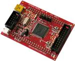
STM32-H152 development board
Users Manual
All boards produced by Olimex are ROHS compliant
Revision Initial, September 2011
Copyright(c) 2011, OLIMEX Ltd, All rights reserved
Page 1
�INTRODUCTION:
STM32-H152 is header board with STM32L152VBT6 ARM Cortex M3 microcontroller from STMicroelectronics. This microcontroller supports various communication interfaces such as USB, three USARTs, two SPIs, two I2C. There are
available mini USB, JTAG and UEXT connectors, two buttons – WKUP and RESET,
two status leds and extension connectors for most of the microcontroller's pins. All
this allows you to build a different projects to be used in a wide range of applications.
BOARD FEATURES:
•
MCU: STM32L152VBT6 – 128 KB Flash, 16 KB Data RAM
•
Mini USB
•
3.7V-LI_BAT connector
•
Battery charger
•
JTAG connector
•
UEXT connector
•
Two status leds
•
Reset circuit
•
RESET button
•
WKUP button
•
Extension connectors for most of the microcontroller pins
•
FR-4, 1.5 mm, soldermask, component print
•
Dimensions: 70.00 x 50.00 mm (2.76 x 1.97")
Page 2
�ELECTROSTATIC WARNING:
The STM32-H152 board is shipped in protective anti-static packaging. The board
must not be subject to high electrostatic potentials. General practice for working
with static sensitive devices should be applied when working with this board.
BOARD USE REQUIREMENTS:
Cables: The cable you will need depends on the programmer/debugger you use. If
you use ARM-JTAG-EW, ARM-USB-TINY or ARM-USB-TINY-H, you will need
USB A-B cable, if you use ARM-USB-OCD or ARM-USB-OCD-H, you will need
USB A-B cable and RS232 cable.
Hardware:
Programmer/Debugger ARM-USB-OCD, ARM-USB-OCD-H,
ARM-USB-TINY, ARM-USB-TINY-H, ARM-JTAG-EW or other compatible
programming/debugging tool if you work with EW-ARM.
PROCESSOR FEATURES:
STM32-H152 board use ARM 32-bit Cortex™-M3 microcontroller
STM32L152VBT6 from STMicroelectronics with these features:
−
−
−
−
−
Operating conditions
−
Operating power supply range: 1.65 V to 3.6 V (without BOR) or 1.8 V to
3.6 V (with BOR option)
−
Temperature range: –40 to 85 °C
Low power features
−
4 modes: Sleep, Low-power run (9 μA at 32 kHz), Low-power sleep (4.4
μA), Stop with RTC (1.45 μA), Stop (570 nA), Standby (300 nA)
−
Dynamic core voltage scaling down to 233 μA/MHz
−
Ultralow leakage per I/O: 50 nA
−
Fast wakeup from Stop: 8 μs
−
Three wakeup pins
Core: ARM 32-bit Cortex™-M3 CPU
−
32 MHz maximum frequency, 33.3 DMIPS peak (Dhrystone 2.1)
−
Memory protection unit
Reset and supply management
−
Low power, ultrasafe BOR (brownout reset) with 5 selectable thresholds
−
Ultralow power POR/PDR
−
Programmable voltage detector (PVD)
Clock management
Page 3
�−
−
1 to 24 MHz crystal oscillator
−
32 kHz oscillator for RTC with calibration
−
Internal 16 MHz factory-trimmed RC
−
Internal 37 kHz low consumption RC
−
Internal multispeed low power RC, 64 kHz to 4 MHz with a consumption
down to 1.5 μA
−
PLL for CPU clock and USB (48 MHz)
Low power calendar RTC
−
−
Alarm, periodic wakeup from Stop/Standby
Memories
−
128 Kbyte of Flash memory with ECC
−
4 Kbyte of data EEPROM with ECC
−
16 Kbyte of RAM
−
83 fast I/Os (73 of which are 5 V-tolerant) all mappable on 16 external interrupt
vectors
−
Development support
−
Serial wire debug, JTAG and trace
−
DMA: 7-channel DMA controller, supporting timers, ADC, SPIs, I2Cs and
USARTs
−
LCD 8 × 40 or 4 × 44 with step-up converter
−
12-bit ADC up to 1 Msps/24 channels
−
Temperature sensor and internal voltage reference
−
Operates down to 1.8 V
−
2× 12-bit DACs with output buffers
−
2 ultralow power comparators
−
−
−
−
Window mode and wakeup capability
10 timers:
−
6 × 16-bit general-purpose timers, each with up to 4 IC/OC/PWM
channels
−
2 × 16-bit basic timers
−
2 × watchdog timers (independent and window)
8 communication interfaces:
−
2 × I2C interfaces (SMBus/PMBus)
−
3 × USARTs (ISO 7816 interface, LIN, IrDA capability, modem control)
−
2 × SPIs (16 Mbit/s)
−
USB 2.0 full speed interface
CRC calculation unit, 96-bit unique ID
Page 4
�Page 5
�BLOCK DIAGRAM:
AF = Alternate Function function on I/O port pin.
Page 6
�MEMORY MAP:
Page 7
�C3 100nF
Page 8
R6
1
2
3
Q1
B0_ 1/B0_ 0
STAT1
STAT2
SPI1_ NSS
SPI1_ SCK
SPI1 _MISO
SPI1 _MO SI
RST
+5V_ USB
R1 4 4 .7k
1 0k
R8
1 uF/10 V
HN1 x3
0
C16
CO N2-6
CO N1-6
NA
100 nF
C1 3 1u F/1 0V
C1 5
C1 4
97
98
1
2
3
4
5
38
39
40
41
42
43
44
45
46
14
73
13
12
94
6
20
21
19
22
STM32L 15 2VBT6
OSC_IN/PD0/SPI2_NSS/TIM9_CH1
OSC_OUT/PD1/SPI2_SCK
PD2/TIM3_ETR/LCD_SEG31/LCD_SEG43/LCD_COM7
PD3/USART2_CTS/SPI2_MISO
PD4/USART2_RTS/SPI2_MOSI
PD5/USART2_TX
PD6/USART2_RX
PD7/USART2_CK/TIM9_CH2
PD8/USART3_TX/LCD_SEG28
PD9/USART3_RX/LCD_SEG29
PD10/USART3_CK/LCD_SEG30
PD11/USART3_CTS/LCD_SEG31
PD12/TIM4_CH1/USART3_RTS/LCD_SEG32
PD13/TIM4_CH2/LCD_SEG33
PD14/TIM4_CH3/LCD_SEG34
PD15/TIM4_CH4/LCD_SEG35
PC0/ADC_IN10/LCD_SEG18/COMP1_INP
PC1/ADC_IN11/LCD_SEG19/COMP1_INP
PC2/ADC_IN12/LCD_SEG20/COMP1_INP
PC3/ADC_IN13/LCD_SEG21/COMP1_INP
PC4/ADC_IN14/LCD_SEG22/COMP1_INP
PC5/ADC_IN15/LCD_SEG23/COMP1_INP
PC6/TIM3_CH1/LCD_SEG24
PC7/TIM3_CH2/LCD_SEG25
PC8/TIM3_CH3/LCD_SEG26
PC9/TIM3_CH4/LCD_SEG27
PC10/USART3_TX/LCD_SEG28/LCD_SEG40/LCD_COM4
PC11/USART3_RX/LCD_SEG29/LCD_SEG41/LCD_COM5
PC12/USART3_CK/LCD_SEG30/LCD_SEG42/LCD_COM6
PC13/RTC_AF1/WKUP2
PC14/OSC32_IN
PC15/OSC32_OUT
PB0/ADC_IN8/TIM3_CH3/LCD_SEG5/COMP1_INP/VREF_OUT
PB1/ADC_IN9/TIM3_CH4/LCD_SEG6/COMP1_INP/VREF_OUT
PB2/BOOT1
JTDO/TIM2_CH2/PB3/TRACESWO/SPI1_SCK/COMP2_INM/LCD_SEG7
JNTRST/TIM3_CH1/PB4/SPI1_MISO/COMP2_INP/LCD_SEG8
PB5/I2C1_SMBAL/TIM3_CH2/SPI1_MOSI/COMP2_INP/LCD_SEG9
PB6/I2C1_SCL/TIM4_CH1/USART1_TX/LCD_SEG8
PB7/I2C1_SDA/TIM4_CH2/USART1_RX/PVD_IN
PB8/TIM4_CH3/I2C1_SCL/LCD_SEG16/TIM10_CH1
PB9/TIM4_CH4/I2C1_SDA/LCD_COM3/TIM11_CH1
PB10/I2C2_SCL/USART3_TX/TIM2_CH3/LCD_SEG10
PB11/I2C2_SDA/USART3_RX/TIM2_CH4/LCD_SEG11
PB12/SPI2_NSS/I2C2_SMBA/USART3_CK/LCD_SEG12/ADC_IN18/COMP1_INP/TIM10_CH1
PB13/SPI2_SCK/USART3_CTS/LCD_SEG13/ADC_IN19/COMP1_INP/TIM9_CH1
PB14/SPI2_MISO/USART3_RTS/LCD_SEG14/ADC_IN20/COMP1_INP/TIM9_CH2
PB15/SPI2_MOSI/TIM1_CH3N/LCD_SEG15/ADC_IN21/COMP1_INP/TIM11_CH1/RTC_50_60HZ
PA0/WKUP1/USART2_CTS/ADC_IN0/TIM2_CH1_ETR/COMP1_INP
PA1/USART2_RTS/ADC_IN1/TIM2_CH2/LCD_SEG0/COMP1_INP
PA2/USART2_TX/ADC_IN2/TIM2_CH3/TIM9_CH1/LCD_SEG1/COMP1_INP
PA3/USART2_RX/ADC_IN3/TIM2_CH4/TIM9_CH2/LCD_SEG2/COMP1_INP
PA4/SPI1_NSS/USART2_CK/ADC_IN4/DAC_OUT1/COMP1_INP
PA5/SPI1_SCK/ADC_IN5/DAC_OUT2/TIM2_CH1_ETR/COMP1_INP
PA6/SPI1_MISO/ADC_IN6/TIM3_CH1/TIM1_BKIN/LCD_SEG3/TIM10_CH1/COMP1_INP
PA7/SPI1_MOSI/ADC_IN7/TIM3_CH2/TIM1_CH1N/LCD_SEG4/TIM11_CH1/COMP1_INP
PA8/USART1_CK/MCO/LCD_COM0
PA9/USART1_TX/LCD_COM1
PA10/USART1_RX/LCD_COM2
PA11/USART1_CTS/USBDM/SPI1_MISO
PA12/USART1_RTS/USBDP/SPI1_MOSI
JTMS/SWDIO/PA13
JTCK/SWCLK/PA14
JTDI/TIM2_CH1_ETR/PA15/SPI1_NSS/LCD_SEG17
PE0/TIM4_ETR/LCD_SEG36/TIM10_CH1
PE1/LCD_SEG37/TIM11_CH1
PE2/TRACECK/LCD_SEG38/TIM3_ETR
PE3/TRACED0/LCD_SEG39/TIM3_CH1
PE4/TRACED1/TIM3_CH2
PE5/TRACED2/TIM9_CH1
PE6/TRACED3/WKUP3/TIM9_CH2
PE7/ADC_IN22/COMP1_INP
PE8/ADC_IN23/COMP1_INP
PE9/ADC_IN24/TIM2_CH1_ETR/COMP1_INP
PE10/ADC_IN25/TIM2_CH2/COMP1_INP
PE11/TIM2_CH3
PE12/TIM2_CH4/SPI1_NSS
PE13/SPI1_SCK
PE14/SPI1_MISO
PE15/SPI1_MOSI
NRST
PH2/I2C2_SMBA
OSC_OUT/PH1
OSC_IN/PH0
BOOT0
VLCD
VREF-
VREF+
VSSA
VDDA
VSS_5
VSS_4
VSS_3
VSS_2
VSS_1
VDD_1
VDD_2
VDD_3
VDD_4
VDD_5
R3 4
1 0k
81
82
83
84
85
86
87
88
55
56
57
58
59
60
61
62
15
16
17
18
33
34
63
64
65
66
78
79
80
7
8
9
35
36
37
89
90
91
92
93
95
96
47
48
51
52
53
54
USART2 _TX
USART2 _RX
R1 7
CO N2 -2 0
CO N2 -21
CO N2-22
CO N2-23
CO N2-2 4
CO N2-2 5
CO N2 -2 6
CO N2 -2 7
CO N2 -28
CO N2 -29
CO N2-30
CO N2 -18
CO N2-19
G ND
TMS/SW DIO
TCK/SW CLK
CO N2-10
CO N2-1 1
CO N2-1 2
CO N2 -1 3
CO N2 -14
CO N2 -15
CO N2 -16
CO N2-17
3.3V
CO N1 -3 6
CO N1 -35 HN2 X40
CO N1 -34
CO N1-33
CO N1-32
CO N1-3 1
CO N1 -3 0
CO N1 -2 9
CO N1 -2 8
CO N1 -27
CO N1-26
CO N1-25
CO N1-2 4
CO N1-2 3
CO N1 -2 2
CO N1 -21
GND
1
2
CLO SE
G NDA_ E
SPI1 _MO SI
SPI1 _MISO
SPI1 _SCK
SPI1 _NSS
USART2_ TX
USART2 _RX
I2 C1 _SCL
I2 C1 _SDA
TRST
TDO
TRST
TDI
TMS/SW DIO
TCK/SW CLK
R21
33 k
3 .3V
C6
R22
4.7 k
RST
R-T
R2
R3
R3 1
22 R
2 2R
3 30 R
2
R9
NA
NA
R1 1
NA
USART2_ RX
I2C1_ SDA
SPI1_ MO SI
SPI1_ NSS
2
4
6
8
10
1
3
5
7
9
BH10 S
UEXT
1
2
3
1 0k
1 0k
10 k
R1 3
NA
R20
4 .7k
3 .3V
USART2 _TX
I2C1_ SCL
SPI1_ MISO
SPI1 _SCK
3 .3V
R18
R19
R1 6
R1 2
NA
C9
1 00 nF
U4
R2 8
10 k
BH2 0S
JTAG
2
4
6
8
10
12
14
16
18
20
3.3 V
1M
1 00 nF
10 0n F
C26
3 30 R
R32
1 00 R/1 %
R30
3 .3 V
RST
STAT1
RED(GYX-SD-TC0805SYRK)
STAT1
R26
3 30 R
STAT2
GREEN(GYX-SD-TC0805SGC)
STAT2
3.3V
R27
3 30 R
3.3V
STATUS LEDS
1
3
5
7
9
11
13
15
17
19
R4
VBUS
DD+
ID
GND
USB
USB_MINI
RESET
C10
GND
NA(S TM1001RW X 6F)
2 VCC RESET 1
+5 V_USB
+5 V_JTAG
JTAG
USBL C6 -2 P6(NA)
6
5
4
U1
10 0n F
C8
3.3 V
USB CIRCUIT
W KUP
UEXT
R1 5
R1 0
NA
47p F(NA)
C7
C2 5
1 00 nF
R29
1 00R/1 %
R3 3
10 0k
O PEN
1
4 7pF(NA)
USB_DP
USB_DM
W KUP
SPI1 _SCK,SPI1 _MO SI,SPI1 _MISO ,SPI1_NSS,I2C1_ SDA,I2C1_ SCL,USART2_ RX,USART2_ TX
USART2_ RX
I2 C1 _SDA
SPI1_ MO SI
SPI1_ NSS
TDO
TRST
TDI
TMS/SW DIO ,TCK/SW CLK,TRST,TDO ,TDI
CO N2 -9
CO N2-8
USB_DP,USB_DM
1
C21
2 .2u F/6.3 V
CO N2-3 1
CO N2-3 2
CO N2 -3 3
CO N2-3 4
CO N2-3 5
CO N2 -3 6
CO N2 -3 7
CO N2 -38
CO N2 -39
CO N2-40
CO N1 -4 0
CO N1 -39
CO N1 -38
CO N1-37 C1 9 10p F
Q2
NA
C20 1 0p F
3 27 68 Hz/6pF
I2C1_ SCL
I2C1_ SDA
PB2 /BO O T1
TDO
TRST
23
W KUP
24 BATTERY_VOLTAGE
25 ENABLE_MEASUREMENT
26
29
30
31
32
67
68
69
USB_DM
70
USB_ DP
71
72
TMS/SW DIO
TCK/SW CL K
76
77
TDI
ENABLE_MEASUREMENT
C2 7
1 00 nF
BATTERY_VOLTAGE
3 .7V-L I_ BAT
DW 0 2R
-
1
2
C22
2 .2u F/6 .3 V
RESET CIRCUIT
GND4
GND3
CO N1 -17
CO N1 -18
CO N1-19
CO N1-2 0
CO N1-7
CO N1-8
CO N1-9
CO N1 -1 0
CO N1 -1 1
CO N1 -12
CO N1 -13
CO N1-14
CO N1-15
CO N1-1 6
C18
2 7p F
C1 2
10 0n F
CO N1 -5
CO N2-5
1
2
3
Q8.000MHz/HC-49SM(SMD)/20pF
C1 7
27 pF
0R(NA)
3.3V
0R
CO N1 -4
CO N2 -4
R5 0R 0 R(NA)
C1 1
1u F/1 0V
10
27
99
74
49
50
75
100
28
11
U2
2.2 uF/6 .3V
C24
R24
3 3k
IRLM L6402
FET1
3
3 .3 V
BUTTONS
3
B1_ 1/B1 _0
HN1x3
C1 100nF
1 0k
C2 2.2uF/6.3V
CO N1-3
FB1 CO N2-3
C4 100nF
0
CL O SE
C5 100nF
FB0805/600R/200mA(201209-601)
1
SHUNT_E
2
3.3 V
5
1
R23
4.7k
VIN
VOUT
3.3 V
USB
PB2/BO O T1
CO N2 -2
CO N1-2
1R
R1
+5V
3
2
M CP1702T -3302E/MB
VR(3 .3V)
GND2
GND1
R7
2
1
15 k
VSSPROG
appr. 70 mA charge current
R2 5
2
BATTERY CE
CHARGER
VDDVBAT
D3
BAT54 C
IT1185AU2
3 .3 V
3 .3V_ MCU_ E
HN1 x2
C23
4
M CP73812T-420I/OT
U3
Battery Charger
D1
BAT54 C
POWER SUPPLY CIRCUIT
+5 V
2 .2 uF/6.3V
D2
BAT54 C
CO N2-7
5 -6VDC
+
CO N2 -1
+5V_ JTAG
+5 V_USB
IT 118 5AU2
CO N1 -1
HN2 X4 0
h ttp ://www.olimex.co m/d ev
CO PYRIG HT(C) 201 1, O L IMEX L td .
Re v. B
STM32-H152
SCHEMATIC:
�BOARD LAYOUT:
Page 9
�POWER SUPPLY CIRCUIT:
STM32-H152 can take power from:
–USB - +5V_USB.
–J-link - +5V_JTAG.
–Battery connector – +3.7V lithium battery.
–Extension connector CON2 pin 7 (VIN) – (5÷6) VDC.
The programmed board power consumption is about 30 mA.
Note that if the battery is connected to 3,7V-Li BAT connector and some of other
power sources(USB, JTAG, CON2 pin 7 (VIN)) are present and the battery is
discharged then the battery will be charged until the charge complete.
RESET CIRCUIT:
STM32-H152 reset circuit includes R28 (10k), R30 (330Ω), R32 (100Ω/1%),
C26 (100nF), STM32L152VBT6 pin 14 (NRST) and RESET button.
CLOCK CIRCUIT:
Quartz crystal (Q1) 8 MHz is connected to STM32L152VBT6 pin 12
(OSC_IN/PH0) and pin 13 (OSC_OUT/PH1).
Quartz crystal (Q2) 32.768 kHz is connected to STM32L152VBT6 pin 8
(PC14/OSC32_IN) and pin 9 (PC15/OSC32_OUT).
JUMPER DESCRIPTION:
R-T
When this jumper is closed, RST and TRST are connected. When this jumper is
opened, RST and TRST are separated.
Default state is opened.
SHUNT_E
When this jumper is closed, 1 Ohm shunt is enabled. When this jumper is opened, 1
Ohm shunt is disabled.
Default state is closed.
GNDA_E
When this jumper is closed, the board analog ground is enabled. When this jumper is
opened, the board analog ground is disabled.
Default state is closed.
3.3V_MCU_E
When this jumper is closed, STM32L152VBT6 power supply is enabled. When this
jumper is opened, STM32L152VBT6 power supply is disabled.
Default state is closed.
Page 10
�B0_1/B0_0
This jumper, when is in position B0_1 – connects STM32L152VBT6 pin 94 (BOOT0) via
R8 (10k) to 3.3V, when the jumper is in position B0_0 – connects STM32L152VBT6 pin
94 (BOOT0) via R8 (10k) to GND.
Default state is closed in position B0_0.
B1_1/B1_0
This jumper, when is in position B1_1 – connects STM32L152VBT6 pin 37
(PB2/BOOT1) via R7 (10k) to 3.3V, when the jumper is in position B1_0 – connects
STM32L152VBT6 pin 37 (PB2/BOOT1) via R7 (10k) to GND.
Default state is closed in position B1_0.
-
B1_1
The boot mode is selected depending on jumpers B0_1/B0_0 and B1_1/B1_0
configuration:
- When B0_1/B0_0 is closed in position B0_0 and B1_1/B1_0 position doesn't matter
the boot mode is Main Flash Memory.
- When B0_1/B0_0 is closed in position B0_1 and B1_1/B1_0 is closed in position B1_0
– the boot mode is System Memory.
- When B0_1/B0_0 is closed in position B0_1 and B1_1/B1_0 is closed in position
– the boot mode is Embedded SRAM.
INPUT/OUTPUT:
Status led (red), with name STAT1 is connected to STM32L152VBT6 pin 41 (PF10).
Status led (green), with name STAT2 is connected to STM32L152VBT6 pin 42
(PF11).
User button with name WKUP is connected to STM32L152VBT6 pin 23
(PA0/WKUP1).
User button with name RESET is connected to STM32L152VBT6 pin 14 (NRST).
Page 11
�EXTERNAL CONNECTORS DESCRIPTION:
UEXT:
Pin #
Signal Name
1
VCC (3.3V)
2
GND
3
USART2_TX
4
USART2_RX
5
I2C1_SCL
6
I2C1_SDA
7
SPI1_MISO
8
SPI1_MOSI
9
SPI1_SCK
10
SPI1_NSS
USB:
Pin #
Signal Name
1
+5V_USB
2
USB_DM
3
USB_DP
4
Not Connected
5
GND
Page 12
�3.7V-LI_BAT:
Pin #
Signal Name
1
VBAT
2
GND
JTAG:
Pin #
Signal Name
Pin #
Signal Name
1
VCC (3.3V)
2
VCC (3.3V)
3
TRST
4
GND
5
TDI
6
GND
7
TMS/SWDIO
8
GND
9
TCK/SWCLK
10
GND
11
Via 10k to GND
12
GND
13
TDO
14
GND
15
RST
16
GND
17
Via 10k to GND
18
GND
19
+5V_JTAG
20
GND
Page 13
�CON1:
Pin #
Signal Name
Pin #
Signal Name
1
VCC (3.3V)
2
GND
3
VDDA
4
AGND
5
VREF+
6
VREF-
7
PE0
8
PE1
9
PE2
10
PE3
11
PE4
12
PE5
13
PE6
14
PE7
15
PE8
16
PE9
17
SPI1_NSS
18
SPI1_SCK
19
SPI1_MISO
20
SPI1_MOSI
21
PD15
22
PD14
23
PD13
24
PD12
25
PD11
26
PD10
27
PD9
28
PD8
29
PD7
30
USART2_RX
31
USART2_TX
32
PD4
33
PD3
34
PD2
35
PD1
36
PD0
37
PC13
38
PC12
39
PC11
40
PC10
Page 14
�CON2:
Pin #
Signal Name
Pin #
Signal Name
1
VCC (3.3V)
2
GND
3
VDDA
4
AGND
5
VREF+
6
VREF-
7
VIN
8
GND
9
VCC (3.3V)
10
PA3
11
PA4
12
PA5
13
PA6
14
PA7
15
PA8
16
PA9
17
PA10
18
PB0
19
PB1
20
PB5
21
I2C1_SCL
22
I2C1_SDA
23
PB8
24
PB9
25
PB10
26
PB11
27
PB12
28
PB13
29
PB14
30
PB15
31
PC0
32
PC1
33
PC2
34
PC3
35
PC4
36
PC5
37
PC6
38
PC7
39
PC8
40
PC9
Page 15
�MECHANICAL DIMENSIONS:
Page 16
�AVAILABLE DEMO SOFTWARE:
Demo software USB mouse and Blinking LED for EW-ARM
Setup GCC+Eclispse for STM32 on MAC
Page 17
�ORDER CODE:
STM32-H152 - assembled and tested board
How to order?
You can order to us directly or by any of our distributors.
Check our web www.olimex.com/dev for more info.
Revision history:
Boar's revision:
Rev. B, June 2011
Manual's revision:
Rev. Initial, September 2011
Page 18
�Disclaimer:
© 2011 Olimex Ltd. All rights reserved. Olimex®, logo and combinations thereof, are registered
trademarks of Olimex Ltd. Other terms and product names may be trademarks of others.
The information in this document is provided in connection with Olimex products. No license, express
or implied or otherwise, to any intellectual property right is granted by this document or in
connection with the sale of Olimex products.
Neither the whole nor any part of the information contained in or the product described in this
document may be adapted or reproduced in any material from except with the prior written
permission of the copyright holder.
The product described in this document is subject to continuous development and improvements. All
particulars of the product and its use contained in this document are given by OLIMEX in good faith.
However all warranties implied or expressed including but not limited to implied warranties of
merchantability or fitness for purpose are excluded.
This document is intended only to assist the reader in the use of the product. OLIMEX Ltd. shall not
be liable for any loss or damage arising from the use of any information in this document or any error
or omission in such information or any incorrect use of the product.
Page 19
�