Page 1 of 3
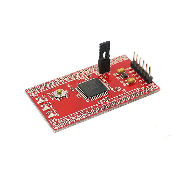
XC9572XL CPLD dev-board introduction
From DP
The development board comes programmed with the inverse LED toggle demo.
1. Ensure that header VIO has a jumper to provide 3.3volts to the IO pins
2. Power up the board:
1. Option 1: Connect a 5volt power supply to V+, connect one of the GND pins to the power
supply ground
2. Option 2: Connect a 3.3volt power supply to VTG on the JTAG header, connect one of the
GND pins to the power supply ground
3. LED D1 will light
4. Press the button (PB): LED D1 turns off and LED D2 turns on
Overview
◾ JTAG header - Program the CPLD through this header. VTG provides 3.3volt output to
programmer
◾ VIO header - Connect IO to on-board 3.3volt supply
◾ D1 LED - User LED connected to pin 39
◾ D2 LED - User LED connected to pin 38
◾ PWR LED - Power LED, lights when the 3.3volt supply is active
◾ PB button - Push button for input, connected to CPLD pin 18
◾ GND pin - Ground connection, only one pin needs to be connected to the power supply ground
◾ V+ pin - Power supply for on-board 3.3volt regulator (5volts max)
◾ 3V3 pin - 3.3volt output (max 100mA)
�Page 2 of 3
◾ IO pin - External supply for IO pins, make sure header VIO has NO jumper, only one IO pin
needs to be connected to the power supply
Pinout table
Pinout
FB4/2
GND
V+
3V3
IO
19
20
21
22
23
27
28
29
30
31
32
33
34
36
37
38
Description
Ground connection
Supply voltage (max 5volts)
3.3volt output (max 100mA)
IO external supply
Description
Ground connection
Supply voltage
IO external supply (1.2-3.3volts)
Push button
LED D2
LED D1
Functional diagram
FB3/FB1
GND
V+
IO
18
16
14
13
12
8
6
5
3
2
1
44
43
42
41
40
39
�Page 3 of 3
Retrieved from "http://dangerousprototypes.com/docs/XC9572XL_CPLD_dev-board_introduction"
Categories: Projects | CPLD development boards | Xilinx
http://dangerousprototypes.com/docs/XC9572XL_CPLD_dev-board_introduction
1/11/2016
�
很抱歉,暂时无法提供与“102990001”相匹配的价格&库存,您可以联系我们找货
免费人工找货