1300 Henley Court
Pullman, WA 99163
509.334.6306
www.digilentinc.com
PmodLVLSHFT™ Reference Manual
Revised April 12, 2016
This manual applies to the PmodLVLSHFT rev. B
Overview
The Digilent PmodLVLSHFT is a digital logic level shifter. This module is ideal for users who want to supply logic
signals following a 3.3V CMOS standard but have an alternate logic level output that is used for other applications
such as JTAG programming.
Digital logic level shifter
Translate logic signals between two user
supplied voltage levels
2×7 JTAG header
8 miniature switches to dictate logic level
conversion
Voltage range between 1.8V and 5.5V
Small PCB size for flexible designs 1.8 in ×
0.8 in (4.6 cm × 2.0 cm)
12-pin Pmod port with GPIO interface
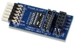
The PmodLVLSHFT.
1
Functional Description
The PmodLVLSHFT translates logic signals between two user supplied voltage levels. Users can use a small object
such as a pen or a screwdriver to adjust the switches for the direction of the voltage translation.
2
Interfacing with the Pmod
The PmodLVLSHFT communicates with the host board via GPIO. Users can supply any form of digital signals to
either end of the Pmod and have them translated to the other voltage level. Switches are provided to indicate the
direction of the voltage translation. A switch pushed to the left side (green) towards the pin header translates
voltages from VCCB to VCCA; a switch on the right side (yellow) towards the JTAG header translates from VCCA to
VCCB.
DOC#: 502-320
Copyright Digilent, Inc. All rights reserved.
Other product and company names mentioned may be trademarks of their respective owners.
Page 1 of 3
�PmodLVLSHFT™ Reference Manual
Figure 1. Switches indicating the voltage direction.
A pinout table for the PmodLVLSHFT is provided below:
Header J1
Pin Signal
1
AIO1/TMS
2
AIO2/TDI
3
AIO3/TDO
4
AIO4/TCK
5
GND
6
VCCA
7
AIO5
8
Description
A1 & TMS
JTAG pin
A2 & TDI
JTAG pin
A3 & TDO
JTAG pin
A4 & TCK
JTAG pin
Power Supply
Ground
Power Supply
side A
JTAG Header J2
Pin Signal
1
GND
2
VCCB
3
GND
4
BIO1/TMS
5
GND
6
BIO4/TCK
I/O pin A5
7
GND
AIO6
I/O pin A6
8
BIO3/TDO
9
AIO7
I/O pin A7
9
GND
10
AIO8
I/O pin A8
10
BIO2/TDI
11
GND
11
GND
12
VCCA
12
(NC)
13
GND
14
SRST
Power Supply
Ground
Power Supply
side A
Description
Power Supply
Ground
Power Supply
side B
Power Supply
Ground
B1 & TMS
JTAG pin
Power Supply
Ground
B4 & TCK
JTAG pin
Power Supply
Ground
B3 & TDO
JTAG pin
Power Supply
Ground
B2 & TDI
JTAG pin
Power Supply
Ground
Not
Connected
Power Supply
Ground
Signal Reset
Header J3
Pin Signal
Description
B1 & TMS
JTAG pin
B5 & Signal
Reset pin
B2 & TDI
JTAG pin
1
BIO1/TMS
2
BIO5/SRST
3
BIO2/TDI
4
BIO6
I/O pin B6
5
BIO3/TDO
B3 & TDO
JTAG pin
6
BIO7
I/O pin B7
7
BIO4/TCK
B4 & TCK
JTAG pin
8
BIO8
I/O pin B8
Header J4
Pin
Signal
1
VCCB
2
GND
Description
Power Supply
side B
Power Supply
Ground
Table 1. Pin descriptions for the PmodLVLSHFT.
Note* Headers J2 and J3 follow the JTAG pin numbering convention as opposed to the Pmod header numbering
convention
Copyright Digilent, Inc. All rights reserved.
Other product and company names mentioned may be trademarks of their respective owners.
Page 2 of 3
�PmodLVLSHFT™ Reference Manual
Any external power applied to the PmodLVLSHFT must be within 1.8V and 5.5V.
3
Physical Dimensions
The pins on the pin header are spaced 100 mil apart. The PCB is 1.75 inches long on the sides parallel to the pins on
the pin header and 0.8 inches long on the sides perpendicular to the pin header.
Copyright Digilent, Inc. All rights reserved.
Other product and company names mentioned may be trademarks of their respective owners.
Page 3 of 3
�
很抱歉,暂时无法提供与“410-320”相匹配的价格&库存,您可以联系我们找货
免费人工找货- 国内价格 香港价格
- 1+176.616491+22.86117