Page 1 of 2
Flash 2 click
From MikroElektonika Documentation
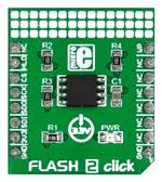
Flash 2 click
Flash 2 click carries Microchip’s SST26VF064B flash-memory module with 8
MB capacity. It’s a highly reliable module with a specified minimum of 100,000
write cycles and with over 100 years of Data Retention. For data security, the
module features a One-Time Programmable (OTP) 2 KB bit secure ID and a 64 bit
unique, factory pre-programmed identifier. Additional software security measures
include inidividual-block write Protection with permanent lock-down capability.
Flash 2 click communicates with the target MCU through the mikroBUS™ SPI
interface (CS#, SCK, MISO, MOSI) with additional functionality provided by the
#HOLD pin (in place of default mikroBUS™ RST pin). The board is designed to
use a 3.3V power supply.
Features and usage notes
The SST26VF064B/064BA
memory array is organized in
uniform, 4 KByte erasable
sectors with the following
erasable blocks:
Flash 2 click
- Eight 8 KB parameter
- Two 32 KByte overlay
- One-hundred twenty-six 64
KByte overlay blocks
Schematic also available in PDF (http://cdndocs.mikroe.com/images/9/96/SchematicFlash_2_click_v100.pdf)
IC/Module Microchip SST26VF064B
(http://ww1.microchip.com/downloads/en/DeviceDoc/20005119G.pdf)
Interface
SPI (MISO, MOSI, SCK), CS, #HOLD
Power
3.3V
supply
The #HOLD pin temporarily
Website
www.mikroe.com/click/flash-2 (http://www.mikroe.com/click/flash-2)
stops serial communication
with the SPI Flash memory
while the device is selected. This pin only works in SPI, single-bit and dual-bit Read mode and must be tied
high when not in use.
The manufacturer's data sheet has more information about the memory protection features of the chip:
"SST26VF064B/064BA offers flexible memory protection scheme that allows the protection state of each individual block to be controlled separately. In
addition, the Write-Protection Lock-Down register prevents any change of the lock status during device operation. To avoid inadvertent writes during power-up,
the device is write-protected by default after a power-on reset cycle. A Global Block Protection Unlock command offers a single command cycle that unlocks the
entire memory array for faster manufacturing throughput."
Programming
This snippet initializes all necessary pins and functions for using Flash 2 Click, and performs a test by writing test values to the click, and then reading them
back to the user through UART communication.
1
2
3
4
5
6
7
8
9
10
11
12
13
14
15
16
17
18
19
20
21
22
23
24
25
26
27
28
29
30
#include
#include "flash_2_hw.h"
sbit FLASH_2_WP at GPIOA_ODR.B0;
sbit FLASH_2_CS at GPIOD_ODR.B13;
sbit FLASH_2_HLD at GPIOC_ODR.B2;
int main(void)
{
uint8_t buffer[4]
uint16_t count
uint32_t address
uint8_t receive_buffer[4];
char tmp[20];
= {15,20,25,30};
= 4;
= 0x0100F0;
GPIO_Digital_Output( &GPIOA_BASE, _GPIO_PINMASK_0 );
GPIO_Digital_Output( &GPIOC_BASE, _GPIO_PINMASK_2 );
GPIO_Digital_Output( &GPIOD_BASE, _GPIO_PINMASK_13 );
SPI1_Init_Advanced( _SPI_FPCLK_DIV64,
_SPI_MASTER | _SPI_8_BIT | _SPI_CLK_IDLE_LOW |
_SPI_FIRST_CLK_EDGE_TRANSITION | _SPI_MSB_FIRST |
_SPI_SS_DISABLE | _SPI_SSM_ENABLE |
_SPI_SSI_1,
&_GPIO_MODULE_SPI3_PC10_11_12 );
Delay_ms(300);
UART1_Init(9600);
�Page 2 of 2
31
32
33
34
35
36
37
38
39
40
41
42
43
44
45
46
47
48
49
50
51
52
53
54
55
56
57
58
59
60 }
Delay_ms(300);
UART1_Write_Text( "Initializing Flash 2 click... " );
UART1_Write_Text( "\r\n" );
flash_2_init();
Delay_ms(300);
flash_2_global_block_unlock();
Delay_ms(400);
flash_2_write( address, buffer, count );
flash_2_read( address, receive_buffer, count );
UART1_Write_Text( "Initial Values: " );
while( count-- )
{
ByteToStr( buffer[count], tmp );
UART1_Write_Text( tmp );
}
UART1_Write_Text( "\r\n" );
count = 4;
UART1_Write_Text( "Received Values: " );
while( count -- )
{
ByteToStr( receive_buffer[count], tmp );
UART1_Write_Text( tmp );
}
UART1_Write_Text( "\r\n" );
return;
Code examples that demonstrate the usage of Flash 2 click with MikroElektronika hardware, written for mikroC for ARM, AVR, dsPIC, FT90x, PIC and PIC32
are available on Libstock (http://libstock.mikroe.com/projects/view/1785/flash-2-click).
Resources
- Microchip SST26VF064B data sheet (http://ww1.microchip.com/downloads/en/DeviceDoc/20005119G.pdf)
- Flash 2 click examples on Libstock (http://libstock.mikroe.com/projects/view/1785/flash-2-click)
- This NAND, NOR that NAND (http://learn.mikroe.com/this-nand-nor-that-nand/), artile about Flash 2 click on learn.mikroe.com
- mikroBUS standard specifications (http://download.mikroe.com/documents/standards/mikrobus/mikrobus-standard-specification-v200.pdf)
Retrieved from "http://docs.mikroe.com/index.php?title=Flash_2_click&oldid=315"
◾ This page was last modified on 18 May 2016, at 19:43.
◾ Content is available under Creative Commons Attribution unless otherwise noted.
http://docs.mikroe.com/index.php?title=Flash_2_click&printable=yes
6/15/2016
�