1300 Henley Court
Pullman, WA 99163
509.334.6306
www.digilentinc.com
PmodAMP3™ Reference Manual
Revised April 15, 2016
This manual applies to the PmodAMP3 rev. A
Overview
The Digilent PmodAMP3 features an Analog Devices® SSM2518 2 watt Class-D Audio Power Amplifier. The module
enables the use of I²S audio protocol or TDM to produce stereo audio at various sampling frequencies. Users may
configure the digital volume and dynamic range control via an I²C interface. Additionally, the PmodAMP3 may be
used in a stand-alone mode that does not require the use of the I²C interface.
Features include:
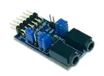
The PmodAMP3.
1
Audio amplifier with left and right channel
separation
Stereo output via two standard 1/8“ (0.32
cm) mono speaker jacks
Supports common I²S audio formats
Digitally configurable volume control for
each channel
Dynamic range control
Stand-alone mode for systems without I²C
interface
Small PCB size for flexible designs 1.5” ×
0.8“ (3.8 cm × 2.0 cm)
12-pin Pmod port with I²C interface
Functional Description
The PmodAMP3 utilizes Analog Devices SSM2518 to reproduce digitally fed audio signals in separate left and right
headphone jacks. The separation of the jacks enables better audio signal isolation.
2
Interfacing with the Pmod
The PmodAMP3 communicates with the host board via the I²C protocol. Users may operate the PmodAMP3 in
either an I²C programmable mode or a simple stand-alone mode. The stand-alone mode is the default setting and
can be activated by removing the shorting block on jumper JP5. When the stand-alone mode is active, jumpers JP3,
JP4, and JP6 allow a simple hardware configuration of the amplifier.
Within the stand-alone mode jumper JP3 configuration determines whether to use Standard or Left Justified I²S
protocol. Jumper JP4 determines if the MCLK input is 256 or 384 times the audio sampling frequency Fs. The
jumper JP6 configures the amplifier to output at either 0dB or +12dB gain.
DOC#: 502-270
Copyright Digilent, Inc. All rights reserved.
Other product and company names mentioned may be trademarks of their respective owners.
Page 1 of 3
�PmodAMP3™ Reference Manual
If JP5 is loaded, I²C is enabled so that the on-board chip can be configured. Consequently, the shorting blocks on
both JP3 and JP4 must be removed so that the SCL and SDA lines are pulled to a logic high voltage state. JP6 sets
the I²C address of the Pmod; both addresses are valid, but a user may want to use one particular address if another
I²C device on the bus is using the other address.
JP5 Unloaded (default Stand-alone mode)
JP5 Loaded (I2C Programmable Mode)
Loaded
MCLK-provide own
external MCLK
Unloaded
BCLK-route BCLK
to MCLK input
Loaded
Unloaded
Don't Care
Don't Care
JP3
JP4
I2S (Standard)
256x Fs
Left Justified
384x Fs
Prohibited
Prohibited
Required
Required
JP6
12dB Gain
0dB Gain
ADDR: 0110100[r/w]
ADDR: 0110110[r/w]
JP2
Table 1. Connector descriptions.
Note: Both the 0dB and +12dB gain modes are very loud. You should take care to protect both yourself and your
equipment when operating in stand-alone mode. Digilent recommends that you use the programmable mode and
set the gain to -12dB or lower.
The I²C programmable mode is used to set alternate Master Clock (MCLK) and Bit Clock (BCLK) ratios as well as
configure the Dynamic Range Control (DRC). More information about these options is available in our user guide.
To transfer audio data in the I²S audio format, the MCLK, BCLK, the Left/Right Word Clock (LRCLK), and the data
(SDATA) will need to be provided either internally or externally as appropriate. This module is able to receive audio
data anywhere between 8 and 32-bits of resolution. An example timing diagram from Texas Instruments on how
I²S data is to be sent to the module is provided below:
Figure 1. Example I2S timing diagram.
Copyright Digilent, Inc. All rights reserved.
Other product and company names mentioned may be trademarks of their respective owners.
Page 2 of 3
�PmodAMP3™ Reference Manual
Pin
1
2
3
4
5
6
7
8
9
10
11
12
Table 2. Header J1 pinout table.
Figure 2. PmodAMP3 block diagram.
Header J2
Pin Description
1
Left Audio
Jack
Signal
LRCLK
SDATA
NC
BCLK
GND
VCC
NC
NC
MCLK-E
~SHUT
GND
VCC
Header J1
Description
Left/Right Word Clock
Serial Data
Not Connected
Bit Clock
Power Supply Ground
Positive Power Supply
Not Connected
Not Connected
Master Clock-external
Shutdown
Power Supply Ground
Positive Power Supply
Header J3
Pin
Description
1
Serial Clock
2
Serial Data
Header J4
Pin Description
1
Right Audio
Jack
Table 3. Header J2, J3, and J4 pinout table.
Any external power applied to the PmodAMP3 must be within 2.5V and 5.5V; however, it is recommended that the
Pmod is operated at 3.3V.
3
Physical Dimensions
The pins on the pin header are spaced 100 mil apart. The PCB is 1.5 inches long on the sides parallel to the pins on
the pin header and 0.8 inches long on the sides perpendicular to the pin header.
Copyright Digilent, Inc. All rights reserved.
Other product and company names mentioned may be trademarks of their respective owners.
Page 3 of 3
�
很抱歉,暂时无法提供与“410-270”相匹配的价格&库存,您可以联系我们找货
免费人工找货- 国内价格 香港价格
- 1+176.837331+22.69023
