Additional Resources:
Product Page
date
01/13/2014
page
1 of 5
SERIES: VHD1-DIP │ DESCRIPTION: DC-DC CONVERTER
1 W isolated output
industry standard 17 pin DIP package
single unregulated outputs
6,000 V isolation
short circuit protection
UL safety approvals
wide temperature (-40~85°C)
efficiency up to 75%
U
•
•
•
•
•
•
•
•
ED
FEATURES
input
voltage
typ
(Vdc)
range
(Vdc)
VHD1-S5-S5-DIP
5
4.5~5.5
VHD1-S5-S9-DIP
5
4.5~5.5
VHD1-S5-S12-DIP
5
4.5~5.5
5
4.5~5.5
VHD1-S12-S5-DIP
12
10.8~13.2
output
current
output
power
ripple
and noise1
efficiency
(Vdc)
min
(mA)
max
(mA)
max
(W)
max
(mVp-p)
typ
(%)
5
20
200
1
150
68
9
12
111
1
150
72
12
9
84
1
150
74
15
7
67
1
150
74
5
20
200
1
150
69
N
VHD1-S5-S15-DIP
output
voltage
TI
MODEL
N
RoHS
12
10.8~13.2
9
12
111
1
150
72
12
10.8~13.2
12
9
84
1
150
74
VHD1-S12-S15-DIP
12
10.8~13.2
15
7
67
1
150
75
1. ripple and noise are measured at 20 MHz BW
IS
C
Notes:
O
VHD1-S12-S9-DIP
VHD1-S12-S12-DIP
D
PART NUMBER KEY
Base Number
VHD1 - SXX - SXX -DIP
Input Voltage
Output Voltage
cui.com
Packaging Style
�Additional Resources:
Product Page
CUI Inc │ SERIES: VHD1-DIP │ DESCRIPTION: DC-DC CONVERTER
date 01/13/2014 │ page 2 of 5
INPUT
conditions/description
min
typ
max
units
operating input voltage
5 V model
12 V model
4.5
10.8
5
12
5.5
13.2
Vdc
Vdc
min
OUTPUT
parameter
conditions/description
line regulation
for Vin change of 1%
load regulation
measured from 10% load to full load
voltage accuracy
see derating curves
switching frequency
100% load, input voltage range
PROTECTIONS
10
conditions/description
min
N
parameter
typ
short circuit protection
SAFETY AND COMPLIANCE
units
%
15
%
kHz
±0.03
%/°C
typ
units
1
s
max
units
conditions/description
for 1 minute at 1 mA max.
6,000
Vdc
isolation resistance
at 500 Vdc
1,000
MΩ
safety approvals
UL 60950 (E222736)
3,500,000
hours
ENVIRONMENTAL
operating temperature
storage temperature
storage humidity
temperature rise
min
typ
max
units
-40
85
°C
-55
125
°C
non-condensing
at full load
15
1.5 mm from case for 10 seconds
D
IS
C
lead temperature
conditions/description
O
parameter
N
yes
TI
parameter
RoHS compliant
typ
max
isolation voltage
MTBF
min
max
±1.2
250
U
temperature coefficient
ED
parameter
cui.com
95
%
25
°C
300
°C
�Additional Resources:
Product Page
CUI Inc │ SERIES: VHD1-DIP │ DESCRIPTION: DC-DC CONVERTER
date 01/13/2014 │ page 3 of 5
DERATING CURVES
2. output voltage vs. output current
ED
1. output power vs. ambient temperature
Load (%)
100
80
60
40
-40
-20
0
20
40
60 71
85
100
U
20
120
MECHANICAL
N
Ambient Temperature (°C)
parameter
conditions/description
dimensions
32.30 x 14.70 x 9.40 (0.768 x 0.396 x 0.492 inch)
case material
plastic (UL94-V0)
MECHANICAL DRAWING
N
units: mm
tolerance: ±0.25
pin section tolerance: ±0.10 mm
O
Side View
9.40
IS
C
0.65
4.00
max
4.2
Layout
24 23
17 16 15 14 13
1 2
8 9 10 1112
g
1.00
2.54
2.54
PIN CONNECTIONS
32.30
24 23
17 16 15 14 13
14.70
1 2
8 9 10 11 1 2
cui.com
units
mm
27.94
Top View
D
typ
TI
weight
min
PIN
FUNCTION
1
+Vin
2
-Vin
8
NC
10
-Vout
12
+Vout
13
+Vout
15
-Vout
17
NC
+ 0.15 / - 0
�Additional Resources:
Product Page
CUI Inc │ SERIES: VHD1-DIP │ DESCRIPTION: DC-DC CONVERTER
date 01/13/2014 │ page 4 of 5
APPLICATION NOTES
Table 1
Input Voltage
External Input
Capacitance
5V
4.7 μF
12 V
2.2 μF
24 V
1.0 μF
+Vin
-Vin
ED
1. Input filtering
To reduce the reflected ripple current and minimize EMI, especially when the converter input is more than 2” away from the DC
source, it is recommended to connect a low ESR electrolytic capacitor between Vin and Gnd. The values suggested are as shown in
Table 1. If additional filtering is required, the capacitance may be increased, or expanded to an LC network as shown in Figure 1.
L
L
C
DC DC
+Vout
C
-Vout
U
Figure 1
External Input
Capacitance
5V
4.7 μF
9V
12 V
-Vin
REG
+Vout
DC DC
-Vout
2.2 μF
1.0 μF
0.47 μF
+Vin
-Vin
REG
DC DC
Figure 2
+Vout
-Vout
N
15 V
+Vin
TI
Table 2
Output Voltage
N
2. Output filtering
An output capacitor is needed to meet output ripple requirements as shown in Table 2. Output capacitance may be increased for additional filtering, but should not exeed 10μF or expanded to an LC network as in Figure 1.
3. Minimum loading
The converter needs a minimum of 10% loading to maintain output regulation. Operation under no-load conditions will not cause immediate damages but may reduce reliability, and cause performance not to meet specifications.
O
4. Regulation
With a semi-regulated design, the converter’s output voltage varies with load current and will change proportionally to the input voltage. If regulated output is needed, an external regulator can be used as shown in Figure 2.
IS
C
5. Protection
The converter has minimal protection against input over-voltage or output over-load, and may be permanently damaged if exposed to
these conditions. An input clamping device can be used for input voltage limiting. An input fuse or an output fuse can also be used to
protect against over-loading.
6. Dual outputs used as a single output
The +Vout and -Vout can be used to obtain a single output that is the sum of the two outputs. In this case, the COM pin shouldn’t be
used.
D
7. External Regulator
An external 3-terminal regulator can be connected to the output of the converter to achieve full regulation. Make sure the converter’s
output voltage provides sufficient head room for the regulator. An additional benefit is that the built-in protection features in the regulator, such as OCP, OTP, etc, will protect the converter also. In a complimentory supply, a negative output regulator must be used to
achieve the negative regulated output.
Note:
All specifications measured at 25°C, humidity
很抱歉,暂时无法提供与“VHD1-S5-S9-DIP”相匹配的价格&库存,您可以联系我们找货
免费人工找货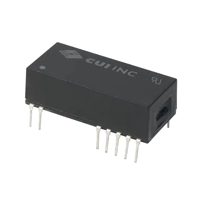


 工商网监
湘ICP备2023018690号
工商网监
湘ICP备2023018690号
