RS30P65D
Lead Free Package and Finish
P-Channel Trench Power MOSFET
General Description
The RS30P65D uses advanced trench technology to provide
excellent RDS(ON), low gate charge and operation with gate
voltages as low as -5V. This device is suitable for use as a
wide variety of applications.
Features
● VDS = -30V,ID =-65A
RDS(ON) < 9mΩ @ VGS =-10V
RDS(ON) < 16mΩ @ VGS =-5V
Schematic Diagram
● High Power and current handing capability
● Lead free product is acquired
● Surface Mount Package
Application
● DC-DC converter
● Load switch
● Power management
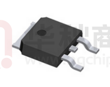
TO-252 top view
100% UIS TESTED!
100% ΔVds TESTED!
Package Marking and Ordering Information
Device Marking
Device
Device Package
RS30P65D
RS30P65D
TO-252
Table 1.
Absolute Maximum Ratings (TA=25℃)
Symbol
Parameter
Value
Unit
-30
V
±25
V
Drain Current-Continuous(Tc=25℃)
-65
A
Drain Current-Continuous(Tc=100℃)
-45
A
-260
A
500
mJ
Maximum Power Dissipation(Tc=25℃)
83
W
Maximum Power Dissipation(Tc=100℃)
41
W
-55 To 175
℃
VDS
Drain-Source Voltage (VGS=0V)
VGS
Gate-Source Voltage (VDS=0V)
ID
IDM (pluse)
EAS
Drain Current-Continuous@ Current-Pulsed
Avalanche energy
(Note 1)
(Note 2)
PD
TJ,TSTG
Operating Junction and Storage Temperature Range
Table 2. Thermal Characteristic
Symbol
RJC
Parameter
Thermal Resistance,Junction-to-Case
Copyright Reasunos
http://www.reasunos.com
Typ
Max
Unit
--
1.8
℃/W
REV:A5 Apr.2019
Page 1 of 6
�RS30P65D
Table 3. Electrical Characteristics (TA=25℃unless otherwise noted)
Symbol
Parameter
Conditions
Min
Typ
Max
Unit
On/Off States
BVDSS
Drain-Source Breakdown Voltage
VGS=0V ID=-250μA
IDSS
Zero Gate Voltage Drain Current
VDS=-30V,VGS=0V
-1
μA
IGSS
Gate-Body Leakage Current
VGS=±25V,VDS=0V
±100
nA
Gate Threshold Voltage
VDS=VGS,ID=-250μA
-1
-1.8
-3
V
VDS=-5V,ID=-10A
20
28
VGS(th)
gFS
RDS(ON)
Forward Transconductance
-30
V
S
VGS=-10V, ID=-20A
7.1
9
mΩ
VGS=-5V, ID=-15A
10
16
mΩ
Drain-Source On-State Resistance
Dynamic Characteristics
Ciss
Input Capacitance
VDS=-15V,VGS=0V,
f=1.0MHz
Coss
Output Capacitance
Crss
Reverse Transfer Capacitance
3570
pF
435
pF
175
pF
16
nS
14
nS
50
nS
Switching Times
td(on)
Turn-on Delay Time
tr
Turn-on Rise Time
td(off)
VDD=-15V,ID=-1A,RL=15Ω
VGS=-10V,RG=2.5Ω
Turn-Off Delay Time
tf
Turn-Off Fall Time
22
nS
Qg
Total Gate Charge
58
nC
Qgs
Gate-Source Charge
9
nC
Qgd
Gate-Drain Charge
14
nC
VGS=-10V, VDS=-15V, ID=-10A
Source-Drain Diode Characteristics
ISD
Source-Drain Current(Body Diode)
VSD
Forward on Voltage
VGS=0V,IS=-10A
-50
A
-1.2
V
Notes 1.Repetitive Rating: Pulse width limited by maximum junction temperature
Notes 2.EAS condition: TJ=25℃,VDD=30V,VG=-10V, RG=25Ω
Copyright Reasunos
http://www.reasunos.com
REV:A5 Apr.2019
Page 2 of 6
�RS30P65D
Switch Time Test Circuit and Switching Waveforms:
TYPICAL ELECTRICAL AND THERMAL CHARACTERISTICS (Curves)
Figure2. Drain Current
-ID Drain Current(A)
Power Dissipation(W)
Figure1. Power Dissipation
TJ-Junction Temperature(℃)
TJ-Junction Temperature(℃)
Figure4. Transfer Characteristics
-Id Drain Current(A)
-Id Drain Current(A)
Figure3. Output Characteristics
-Vds Drain-Source Voltage (V)
Copyright Reasunos
http://www.reasunos.com
-Vgs Gate-Source Voltage (V)
REV:A5 Apr.2019
Page 3 of 6
�RS30P65D
Figure6. RDS(ON) vs Junction Temperature
C Capacitance(pF)
Figure5. Capacitance
-VDS Drain-to-Source Voltage(V)
Figure7. Max BVDSS vs Junction Temperature
Figure8. VGS(th) vs Junction Temperature
Figure10. Maximum Safe Operating Area
-Vgs (V)
-Id(Amds)
Figure9. Gate Charge Waveforms
-Vds(Vlots)
Qg(nC)
Copyright Reasunos
http://www.reasunos.com
REV:A5 Apr.2019
Page 4 of 6
�RS30P65D
Figure11. Normalized Maximum Transient Thermal Impedance
TO-252 Package Information
Copyright Reasunos
http://www.reasunos.com
REV:A5 Apr.2019
Page 5 of 6
�RS30P65D
Disclaimers:
Reasunos Semiconductor Technology CO.,LTD(Reasunos)reserves the right to make changes
without notice in order to improve reliability,function or design and to discontinue any product
or service without notice .Customers should obtain the latest relevant information before orders
and should verify that such information in current and complete.All products are sold subject to
Reasunos's terms and conditions supplied at the time of order acknowledgement.
Reasunos Semiconductor Technology CO.,LTD warrants performance of its hardware products
to the speciffications at the time of sale.Testing,reliability and quality control are used to
the extene Reasunos deems necessary to support this warrantee. Except where agreed upon by contractual agreement,testing of all parameters of each product is not necessarily performed.
Reasunos Semiconductor Technology CO.,LTD does not assume any liability arising from
the use of any product or circuit designs described herein.Customers are responsible for their
products and applications using Reasunos's components.To minimize risk,customers must provide
adequate design and operating safeguards.
Reasunos Semiconductor Technology CO.,LTD does not warrant or convey any license either expressed or implied under its patent rights,nor the rights of others.Reproduction of information in Reasunos's data sheeets or data books is permissible only if reproduction is without
modification oralteration.Reproduction of this information with any alteration is an unfair and
deceptive business practice. Reasunos Semiconductor Technology CO.,LTD is not responsible or liable for such altered documentation.
Resale of Reasunos's products with statements different from or beyond the parameters stated
by Reasunos Semiconductor Technology CO.,LTD for that product or service voids all express or implied warrantees for the associated Reasunos's product or service and is unfair and
deceptive business practice. Reasunos Semiconductor Technology CO.,LTD is not responsible or liable for such statements.
Life Support Policy:
Reasunos Semiconductor Technology CO.,LTD's Products are not authorized for use as critical components in life support devices or systems without the expressed written approval of
Reasunos Semiconductor Technology CO.,LTD.
As used herein:
1.Life support devices or systems are devices or systems which:
a.are intended for surgical implant into the human body,
b.support or sustain life,
c.whose failuer to when properly used in accordance with instructions for used provided
in the laeling,can be reasonably expected to result in significant injury to the user.
2.A critical component is any component of a life support device or system whose failure to
system whose failure to perform can be reasonably expected to cause the failure of the life
support device or system,or to affect its safety or effectiveness.
Copyright Reasunos
http://www.reasunos.com
REV:A5 Apr.2019
Page 6 of 6
�
很抱歉,暂时无法提供与“RS30P65D”相匹配的价格&库存,您可以联系我们找货
免费人工找货- 国内价格
- 1+0.75400
- 10+0.69600
- 30+0.68440
- 100+0.64960