ISD4003 SERIES
SINGLE-CHIP, MULTIPLE-MESSAGES
VOICE RECORD/PLAYBACK DEVICES
4-, 5-, 6-, AND 8-MINUTE DURATION
-1-
Publication Release Date: January 2004
Revision 1.0
�ISD4003 SERIES
1. GENERAL DESCRIPTION
The ISD4003 ChipCorder® series provides high-quality, 3-volt, single-chip record/playback solutions
for 4- to 8-minute messaging applications ideally for cellular phones and other portable products. The
CMOS-based devices include an on-chip oscillator, anti-aliasing filter, smoothing filter, AutoMute®
feature, audio amplifier, and high density multilevel Flash memory array. The ISD4003 series is
designed to be used in a microprocessor- or microcontroller-based system. Address and control are
accomplished through a Serial Peripheral Interface (SPI) or Microwire Serial Interface to minimize pin
count.
Recordings are stored into the on-chip Flash memory cells, providing zero-power message storage.
This unique single-chip solution utilizes Winbond’s patented multilevel storage technology. Voice and
audio signals are directly stored onto memory array in their natural form, providing high-quality voice
reproduction.
-2-
�ISD4003 SERIES
2. FEATURES
•
Single-chip voice record/playback solution
•
Single 3 volt supply
•
Low-power consumption
Operating current:
-
ICC_Play = 15 mA (typical)
-
ICC_Rec = 25 mA (typical)
Standby current:
-
ICC_Standby = 1 µA (typical)
•
Duration: 4, 5, 6, and 8 minutes
•
High-quality, natural voice/audio reproduction
•
AutoMute feature provides background noise attenuation
•
No algorithm development required
•
Microcontroller SPI or Microwire™ Serial Interface
•
Fully addressable to handle multiple messages
•
Non-volatile message storage
•
100K record cycles (typical)
•
100-year message retention (typical)
•
On-chip oscillator
•
Power-down feature to reduce power consumption
•
Available in die form, PDIP, SOIC, and TSOP
•
Temperature:
-
Commercial (die): 0°C to +50°C
-
Commercial (packaged units): 0°C to +70°C
-
Extended: -20°C to +70°C
-
Industrial: -40°C to +85°C
-3-
Publication Release Date: January 2004
Revision 1.0
�ISD4003 SERIES
3. BLOCK DIAGRAM
Internal Clock
Timing
XCLK
Sampling Clock
ANA IN-
Amp
5-Pole Active
Antialiasing Filter
Analog Transceivers
Decoders
ANA IN+
1920K Cell
Nonvolatile
Multilevel Storage
Array
5-Pole Active
Smoothing Filter
AutoMuteTM
Feature
Amp
Power Conditioning
VCCA
VSSA VSSA VSSA VSSD VCCD
Device Control
SCLK
SS
MOSI MISO
-4-
INT
RAC
AM CAP
AUDOUT
�ISD4003 SERIES
4. TABLE OF CONTENTS
1. GENERAL DESCRIPTION.................................................................................................................. 2
2. FEATURES ......................................................................................................................................... 3
3. BLOCK DIAGRAM .............................................................................................................................. 4
4. TABLE OF CONTENTS ...................................................................................................................... 5
5. PIN CONFIGURATION ....................................................................................................................... 6
6. PIN DESCRIPTION ............................................................................................................................. 7
7. FUNCTIONAL DESCRIPTION.......................................................................................................... 12
7.1. Detailed Description.................................................................................................................... 12
7.2. Serial Peripheral Interface (SPI) Description.............................................................................. 13
7.2.1. OPCODES ........................................................................................................................... 14
7.2.2. SPI Diagrams ....................................................................................................................... 15
7.2.3. SPI Control and Output Registers........................................................................................ 16
8. TIMING DIAGRAMS.......................................................................................................................... 18
9. ABSOLUTE MAXIMUM RATINGS.................................................................................................... 20
9.1. Operating Conditions .................................................................................................................. 21
10. ELECTRICAL CHARACTERISTICS ............................................................................................... 22
10.1. Parameters For Packaged Parts ........................................................................................ 22
10.2. Parameters For Die .............................................................................................................. 25
10.3. SPI AC Parameters .............................................................................................................. 26
11. TYPICAL APPLICATION CIRCUIT ................................................................................................. 27
12. PACKAGING AND DIE INFORMATION ......................................................................................... 30
12.1. 28-Lead 300-Mil Plastic Small Outline IC (SOIC)..................................................................... 30
12.2. 28-Lead 600-Mil Plastic Dual Inline Package (PDIP) ............................................................... 31
12.3. 28-Lead 8x13.4mm Plastic Thin Small Outline Package (TSOP) Type 1 ................................ 32
12.4. Die Information ......................................................................................................................... 33
13. ORDERING INFORMATION........................................................................................................... 35
14. VERSION HISTORY ....................................................................................................................... 36
-5-
Publication Release Date: January 2004
Revision 1.0
�ISD4003 SERIES
5. PIN CONFIGURATION
SCLK
SS
1
28
MOSI
2
27
VCCD
MISO
3
26
XCLK
VSSD
4
25
INT
NC
5
24
RAC
NC
6
23
VSSA
NC
7
22
NC
NC
8
21
NC
NC
9
20
NC
NC
10
19
NC
ISD4003
VSSA
11
18
VCCA
VSSA
12
17
ANA IN+
AUD OUT
13
16
ANA IN-
AM CAP
14
15
NC
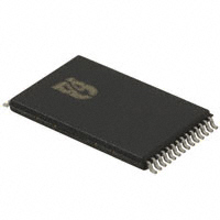
SOIC / PDIP
VSSA
RAC
NC
NC
INT
XCLK
VCCD
SCLK
SS
MOSI
MISO
VSSD
NC
NC
1
28
2
27
3
26
4
25
5
24
6
23
7
8
ISD4003
22
21
9
20
10
19
11
18
12
17
13
16
14
15
TSOP
-6-
NC
NC
VCCA
ANA IN+
ANA INNC
AM CAP
NC
AUD OUT
NC
VSSA
VSSA
NC
NC
�ISD4003 SERIES
6. PIN DESCRIPTION
PIN NAME
PIN NO.
FUNCTION
SOIC /
PDIP
TSOP
SS
1
9
Slave Select: This input, when LOW, will select the
ISD4003 device.
MOSI
2
10
Master Out Slave IN: This is the serial input to the
ISD4003 device when it is configured as slave. The master
microcontroller places data on the MOSI line one half-cycle
before the rising edge of SCLK for clocking into the device.
MISO
3
11
Master In Slave Out: This is the serial output (open drain)
of the ISD4003 device. This output goes into a highimpedance state if the device is not selected.
VSSA / VSSD
11, 12,
23 / 4
1, 17, 18 /
12
Ground: The ISD4003 series utilizes separate analog and
digital ground busses. The analog ground (VSSA) pins
should be tied together as close as possible and connected
through a low-impedance path to power supply ground.
The digital ground (VSSD) pin should be connected through
a separate low-impedance path to power supply ground.
These ground paths should be large enough to ensure that
the impedance between the VSSA pins and the VSSD pin is
less than 3 Ω. The backside of the die is connected to VSS
through the substrate. For chip-on-board design, the die
attach area must be connected to VSS or left floating.
NC
5-10, 15,
19-22
3, 4, 1316, 19, 21,
23, 27, 28
Not connected
AUD OUT [1]
13
20
Audio Output: This pin provides an audio output of the
stored data and is recommended be AC coupled. It is
capable of driving a 5 KΩ impedance REXT.
[1]
The AUD OUT pin is always at 1.2 volts when the device is powered up. When in playback, the output buffer
connected to this pin can drive a load as small as 5 KΩ. When in record, a built-in resistor connects AUD OUT to
the internal 1.2-volt analog ground supply. This resistor is approximately 850 KΩ, but will vary somewhat
according to the sample rate of the device. This relatively high impedance allows this pin to be connected to an
audio bus without loading it down.
-7-
Publication Release Date: January 2004
Revision 1.0
�ISD4003 SERIES
PIN NAME
AM CAP
PIN NO.
FUNCTION
SOIC /
PDIP
TSOP
14
22
AutoMute™ Feature: The AutoMute feature only applies
for playback operation and helps to minimize noise (with 6
dB of attenuation) when there is no signal (i.e. during
periods of silence). A 1 µF capacitor to ground is
recommended to connect to the AM CAP pin.
This capacitor becomes a part of an internal peak detector
which senses the signal amplitude. This peak level is
compared to an internally set threshold to determine the
AutoMute trip point. For large signals, the AutoMute
attenuation is set to 0 dB automatically but 6 dB of
attenuation occurs for silence. The 1 µF capacitor also
affects the rate at which the AutoMute feature changes with
the signal amplitude (or the attack time).
The AutoMute feature can be disabled by connecting the
AM CAP pin directly to VCCA..
ANA IN-
16
24
Inverting Analog Input: This pin transfers the signal into
the device during recording via differential-input mode.
In this differential-input mode, a 16 mVp-p maximum input
signal should be capacitively coupled to ANA IN- for
optimal signal quality, as shown in Figure 1: ANA IN
Modes. This capacitor value should be equal to that used
on ANA IN+ pin. The input impedance at ANA IN- is
normally 56 KΩ.
In the single-ended mode, ANA IN- should be capacitively
coupled to VSSA through a capacitor equal to that used on
the ANA IN+ pin.
ANA IN+
17
25
Non-Inverting Analog Input: This pin is the non-inverting
analog input that transfers the signal to the device for
recording. The analog input amplifier can be driven single
ended or differentially.
In the single-ended input mode, a 32 mVp-p (peak-to-peak)
maximum signal should be capacitively connected to this
pin for optimal signal quality. The external capacitor
associated with ANA IN+ together with the 3 KΩ input
impedance are selected to give cutoff at the low frequency
end of the voice passband.
In the differential-input mode, the maximum input signal at
ANA IN+ should be 16 mVp-p capacitively coupled for
optimal signal quality. The circuit connections for the two
modes are shown in Figure 1.
-8-
�ISD4003 SERIES
PIN NAME
PIN NO.
FUNCTION
SOIC /
PDIP
TSOP
VCCA / VCCD
18 / 27
26 / 7
Supply Voltage: To minimize noises, the analog and digital
circuits in the ISD4003 devices use separate power
busses. These +3V busses are brought out to separate
pins and should be tied together as close to the supply as
possible. In addition, these supplies should be decoupled
as close to the package as possible.
RAC
24
2
Row Address Clock: This is an open drain output that
provides the signal of a ROW with a 200 ms period for 8
KHz sampling frequency. (This represents a single row of
memory.) This signal stays HIGH for 175 ms and stays
LOW for 25 ms when it reaches the end of a row.
The RAC pin stays HIGH for 109.37 µsec and stays LOW
for 15.63 µsec in Message Cueing mode (see Message
Cueing section for detailed description). Refer to the AC
Parameters table for RAC timing information at other
sample rates.
When a record command is first initiated, the RAC pin
remains HIGH for an extra TRACL period. This is due to the
need of loading the internal sample and hold circuits in the
device. This pin can be used for message management
techniques.
A pull-up resistor is required to connect this pin to other
device.
INT
25
5
Interrupt: This is an open drain output pin. This pin goes
LOW and stays LOW when an Overflow (OVF) or End of
Message (EOM) marker is detected. Each operation that
ends with an EOM or OVF will generate an interrupt. The
interrupt will be cleared the next time an SPI cycle is
initiated. The interrupt status can also be read by an RINT
instruction.
A pull-up resistor is required to connect this pin to other
device.
Overflow Flag (OVF) – The Overflow flag indicates that the
end of memory has been reached during a record or
playback operation.
End of Message (EOM) – The End of Message flag is set
only during playback operation when an EOM is found.
There are eight EOM flag position options per row.
-9-
Publication Release Date: January 2004
Revision 1.0
�ISD4003 SERIES
PIN NAME
XCLK
PIN NO.
FUNCTION
SOIC /
PDIP
TSOP
26
6
External Clock Input: The pin has an internal pull-down
device. The ISD4003 series is configured at the factory with
an internal sampling clock frequency centered to ±1
percent of specification. The frequency is then maintained
to a variation of ±2.25 percent over the entire commercial
temperature and operating voltage ranges. The internal
clock has a –6/+4 percent tolerance over the extended
temperature, industrial temperature and voltage ranges. A
regulated power supply is recommended for industrial
temperature range parts. If greater precision is required,
the device can be clocked through the XCLK pin as follows:
Sample Rate
Required Clock
ISD4003-04M
Part Number
8.0 kHz
1024 kHz
ISD4003-05M
6.4 kHz
819.2 kHz
ISD4003-06M
5.3 kHz
682.7 kHz
ISD4003-08M
4.0 kHz
512 kHz
These recommended clock rates should not be varied
because the anti-aliasing and smoothing filters are fixed.
Otherwise, aliasing problems can occur if the sample rate
differs from the one recommended. The duty cycle on the
input clock is not critical, as the clock is immediately
divided by two. If the XCLK is not used, this input must
be connected to ground.
SCLK
28
8
Serial Clock: This is the input clock to the ISD4003 device.
It is generated by the master device (typically
microcontoller) and is used to synchronize the data transfer
in and out of the device through the MOSI and MISO lines,
respectively. Data is latched into the ISD4003 on the rising
edge of SCLK and shifted out of the device on the falling
edge of SCLK.
- 10 -
�ISD4003 SERIES
Internal to the device
53KΩ
0.1 µ F
Signal
3KΩ
ANA IN+
32m Vp-p
To Filter
+
0.1 µ F
3KΩ
ANA IN-
53KΩ
1.2V
Single-Ended Input Mode
Internal to the device
53KΩ
0.1 µ F
3KΩ
ANA IN+
Input Signal
16m Vp-p
-
Input Signal
16m Vp-p
180°
+
To Filter
0.1 µ F
3KΩ
ANA IN-
53KΩ
1.2V
Differential Input Mode
FIGURE 1: ISD4003 SERIES ANA IN MODES
TRAC
(200 ms)
RAC
25 ms
TRACL
FIGURE 2: RAC TIMING WAVEFORM DURING NORMAL OPERATION
(example of 8KHz sampling rate)
- 11 -
Publication Release Date: January 2004
Revision 1.0
�ISD4003 SERIES
7. FUNCTIONAL DESCRIPTION
7.1. DETAILED DESCRIPTION
Audio Quality
The Winbond’s ISD4003 ChipCorder® series is offered at 8.0, 6.4, 5.3 and 4.0 kHz sampling
frequencies, allowing the user a choice of speech quality options. Increasing the sampling frequency
will produce better sound quality, but affects duration. Please refer to Table 1: Product Summary for
details.
Analog speech samples are stored directly into on-chip non-volatile memory without the digitization
and compression associated with other solutions. Direct analog storage provides higher quality
reproduction of voice, music, tones, and sound effects than other solid-state solutions.
Duration
The ISD4003 Series is a single-chip solution with 4-, 5-, 6-, and 8-minute duration.
TABLE 1: PRODUCT SUMMARY OF ISD4003 SERIES
Part Number
Duration
(Minutes)
Sample Rate
(kHz)
Typical Filter Pass
Band (kHz) *
ISD4003-04M
4
8.0
3.4
ISD4003-05M
5
6.4
2.7
ISD4003-06M
6
5.3
2.3
ISD4003-08M
8
4.0
1.7
* This is the –3dB point. This parameter is not checked during production testing and may vary due to process
variations and other factors. Therefore, the customer should not rely upon this value for testing purposes.
Flash Storage
The ISD4003 series utilizes on-chip Flash memory, providing zero-power message storage. The
message is retained for up to 100 years typically without power. In addition, the device can be rerecorded typically over 100,000 times.
Memory Architecture
The ISD4003 series contains a total of 1,920K Flash memory cells, which is organized as 1,200 rows
of 1,600 cells each.
- 12 -
�ISD4003 SERIES
Microcontroller Interface
A four-wire (SCLK, MOSI, MISO & SS ) SPI interface is provided for controlling and addressing
functions. The ISD4003 is configured to operate as a peripheral slave device, with a microcontrollerbased SPI bus interface. Read and write operations are controlled through this SPI interface. An
interrupt signal ( INT ) and internal read only Status Register are provided for handshake purposes.
Programming
The ISD4003 series is also ideal for playback-only applications, where single- or multiple-messages
playback is controlled through the SPI port. Once the desired message configuration is created,
duplicates can easily be generated via a programmer.
7.2. SERIAL PERIPHERAL INTERFACE (SPI) DESCRIPTION
The ISD4003 series operates via SPI serial interface with the following protocol.
First, the data transfer protocol assumes that the microcontroller’s SPI shift registers are clocked on
the falling edge of the SCLK. However, for the ISD4003, the protocols are as follows:
1. All serial data transfers begin with the falling edge of SS pin.
2.
SS is held LOW during all serial communications and held HIGH between instructions.
3. Data is clocked in on the rising edge of the SCLK signal and clocked out on the falling edge of
the SCLK signal, with LSB first.
4. Playback and record operations are initiated when the device is enabled by asserting the SS
pin LOW, shifting in an opcode and an address data to the ISD4003 device (refer to the
Opcode Summary in the following page).
5. The opcodes contain and .
6. Each operation that ends with an EOM or Overflow will generate an interrupt. The Interrupt
will be cleared the next time a SPI cycle is initiated.
7. As Interrupt data is shifted out of the MISO pin, control and address data are simultaneously
shifted into the MOSI pin. Care should be taken such that the data shifted in is compatible
with current system operation. Because it is possible to read an interrupt data and start a new
operation within the same SPI cycle.
8. An operation begins with the RUN bit set and ends with the RUN bit reset.
9. All operations begin after the rising edge of SS .
- 13 -
Publication Release Date: January 2004
Revision 1.0
�ISD4003 SERIES
7.2.1. OPCODES
The available Opcodes are summarized as follows:
TABLE 2: OPCODE SUMMARY
Instructions
OpCodes
Address (11 bits)
POWERUP
Descriptions
Control bits (5 bits)
C0 C1 C2 C3 C4
0
0
1
0
0
Power-Up: Device will be ready for an operation after
TPUD.
0
0
1
1
1
Initiates playback from address .
0
1
1
1
1
Playback from the current address (until EOM or OVF).
0
0
1
0
1
Initiates a record operation from address .
0
1
1
0
1
Records from current address until OVF is reached or
Stop command is sent.
1
0
1
1
1
Initiates Message Cueing (MC) from address .
MC [1]
1
1
1 1
1
Performs a Message Cueing from current location.
Proceeds to the end of message (EOM) or enters OVF
condition if no more messages are present.
STOP
0
1
1
X
0
Stops the current operation.
STOPPWRDN
X
1
0
X
0
Stops the current operation and enters into standby
(power-down) mode.
RINT [2]
0
1
1
X
0
Read Interrupt status bits: Overflow and EOM.
SETPLAY
PLAY
SETREC
REC
SETMC
Notes:
C0 = Message cueing
C1 = Ignore address bit
C2 = Master power control
C3 = Record or playback operation
C4 = Enable or disable an operation
[1]
Message Cueing can be selected only at the beginning of a playback operation.
[2]
As the Interrupt data is shifted out of the ISD4003, control and address data are being shifted in. Care should
be taken such that the data shifted in is compatible with current system operation. It is possible to read interrupt
data and start a new operation at the same time. See Figures 5 - 8 for references.
- 14 -
�ISD4003 SERIES
7.2.2. SPI Diagrams
MOSI
Input Shift Register
(Loaded to Row Counter
A0-A10
only if IAB = 0)
Select Logic
Row Counter
P0-P10
OVF EOM
MISO
Output Shift Register
FIGURE 3: SPI INTERFACE SIMPLIFIED BLOCK DIAGRAM
The following diagram describes the SPI port and the control bits associated with it.
MISO
OVF EOM
P0
P1
P2
P3
P4
P5
P6
P7
P8
P9
P10
0
0
LSB
MOSI
A0
0
MSB
A1
A2
A3
A4
A5
A6
A7
A8
A9
A10
C0
C1
C2
C3
C4
Message Cueing (MC)
Ignore Address Bit (IAB)
Power Up (PU)
Play/Record (P/R)
RUN
FIGURE 4: SPI PORT
- 15 -
Publication Release Date: January 2004
Revision 1.0
�ISD4003 SERIES
7.2.3. SPI Control and Output Registers
The SPI control register provides control of individual function such as play, record, message cueing,
power-up, power-down, start, stop and ignore address pointer operations.
TABLE 3: SPI CONTROL REGISTERS
Control Bit
Control Register
C0
MC
C1
C2
C3
C4
Address Bits
IAB
Bit
Device Function
Message Cueing function
=
1
Enable Message Cueing
=
0
Disable Message Cueing
[1]
Ignore Address bit
=
1
Ignore input address register (A0-A10)
=
0
Use the input address register (A0-A10)
Power Up
PU
=
1
Power-Up
=
0
Power-Down
P/ R
Playback or Record
=
1
Play
=
0
Record
Enable or Disable an operation
RUN
=
1
Start
=
0
Stop
A0-A10
Input address register
TABLE 4: SPI OUTPUT REGISTERS
Output Bits
Description
OVF
Overflow
EOM
End-of-Message
P0-P10
Output of the row pointer register
[1]
When IAB (Ignore Address Bit) is set to 0, a playback or record operation starts from address (A0-A10). For
consecutive playback or record, IAB should be changed to a 1 before the end of that row (see RAC timing).
Otherwise the ISD4003 will repeat the operation from the same row address. For memory management, the Row
Address Clock (RAC) signal and IAB can be used to move around the memory segments.
- 16 -
�ISD4003 SERIES
Message Cueing
Message cueing (MC) allows the user to skip through messages, without knowing the actual physical
location of the messages. It will stop when an EOM marker is reached. Then, the internal address
counter will point to the next message. Also, it will enter into OVF condition when it reaches the end of
memory. In this mode, the messages are skipped 1,600 times faster than the normal playback
mode.
Power-Up Sequence
The ISD4003 will be ready for an operation after power-up command is sent and followed by the TPUD
timing (25 ms for 8 KHz sampling rate). Refer to the AC timing table for other TPUD values with respect
to different sampling rates.
The following sequences are recommended for optimized Record and Playback operations.
Record Mode
1. Send POWERUP command.
2. Wait TPUD (power-up delay).
3. Send POWERUP command.
4. Wait 2 x TPUD (power-up delay).
5. a). Send SETREC command with address xx, or
b). Send REC command (recording from current location).
6. Send STOP command to stop recording.
7. Wait TSTOP/PAUSE.
For 3 & 4), please refer to Apps Brief 39A: recorded pop elimination in the ISD4000 series.
For 5.a), the device will start recording at address xx and will generate an interrupt when an overflow
(end of memory array) is reached, if no STOP command is sent before that. Then, it will automatic
stop recording operation.
Playback Mode
1. Send POWERUP command
2. Wait TPUD (power-up delay)
3. a). Send SETPLAY command with address xx, or
b). Send PLAY command (playback from current location).
4. a). Send STOP command to halt the playback operation, or
b). Wait for playback operation to stop automatically, when an EOM or OVF is reached.
5. Wait TSTOP/PAUSE.
For 3.a), the device will start playback at address xx and it will generate an interrupt when an EOM or
OVF is reached. It will then stop playback operation.
- 17 -
Publication Release Date: January 2004
Revision 1.0
�ISD4003 SERIES
8. TIMING DIAGRAMS
T SSH
SS
T SSm in
T SCKhi
T SSS
SCLK
T DIS
T DIH
T SCKlow
M OSI
T PD
(TRISTATE)
M ISO
T PD
T DF
LSB
FIGURE 5: TIMING DIAGRAM
SS
SCLK
LSB
A8
MOSI
A9
A10
C0
C1
C2
C3
C4
LSB
MISO
OVF
EOM
P0
P1
P2
P3
P4
FIGURE 6: 8-BIT COMMAND FORMAT
- 18 -
P5
�ISD4003 SERIES
SS
SCLK
MOSI
MISO
LSB
A0
A1
A2
LSB
OVF EOM P0
A3
P1
P2
A4
A5
P3
A6
P4
A7
P5
A8
P6
A9
P7
P8
A10 C0
P9
C1
P10 X
C2
C3
X
C4
X
≈ ≈
≈
≈
Data
Stop
≈ ≈
≈
≈ ≈
≈
Play/Record
≈
MISO
≈
MOSI
≈ ≈
SCLK
≈ ≈
SS
≈
FIGURE 7: 16-BIT COMMAND FORMAT
Data
TSTOP/PAUSE
ANA IN
≈
(Rec)
TSTOP/PAUSE
ANA OUT
≈
(Play)
FIGURE 8: PLAYBACK/RECORD AND STOP CYCLE
- 19 -
Publication Release Date: January 2004
Revision 1.0
�ISD4003 SERIES
9. ABSOLUTE MAXIMUM RATINGS
TABLE 5: ABSOLUTE MAXIMUM RATINGS (PACKAGED PARTS)
CONDITIONS
VALUES
Junction temperature
150°C
Storage temperature range
-65°C to +150°C
Voltage applied to any pin
(VSS –0.3V) to (VCC +0.3V)
Voltage applied to any pin (Input current limited to ±20mA)
(VSS –1.0V) to (VCC +1.0V)
Voltage applied to MOSI, SCLK, and SS pins
(VSS –1.0V) to 5.5V
(Input current limited to ±20mA)
Lead temperature (soldering – 10 seconds)
300°C
VCC – VSS
-0.3V to +7.0V
TABLE 6: ABSOLUTE MAXIMUM RATINGS (DIE)
CONDITIONS
VALUES
Junction temperature
150°C
Storage temperature range
-65°C to +150°C
Voltage applied to any pad
(VSS –0.3V) to (VCC +0.3V)
Voltage applied to any pad (Input current limited to ±20 mA)
(VSS –1.0V) to (VCC +1.0V)
Voltage applied to MOSI, SCLK, and SS pins
(VSS –1.0V) to 5.5V
(Input current limited to ±20mA)
VCC – VSS
-0.3V to +7.0V
Note: Stresses above those listed may cause permanent damage to the device. Exposure to the absolute
maximum ratings may affect device reliability and performance. Functional operation is not implied at these
conditions.
- 20 -
�ISD4003 SERIES
9.1. OPERATING CONDITIONS
TABLE 7: OPERATING CONDITIONS (PACKAGED PARTS)
CONDITIONS
VALUES
Commercial operating temperature range (Case temperature)
0°C to +70°C
Extended operating temperature (Case temperature)
-20°C to +70°C
Industrial operating temperature (Case temperature)
-40°C to +85°C
Supply voltage (VCC)
Ground voltage (VSS)
[1]
+2.7V to +3.3V
[2]
0V
TABLE 8: OPERATING CONDITIONS (DIE)
CONDITIONS
VALUES
Commercial operating temperature range
Supply voltage (VCC)
Ground voltage (VSS)
[1]
VCC = VCCA = VCCD
[2]
VSS = VSSA = VSSD
0°C to +50°C
[1]
+2.7V to +3.3V
[2]
0V
- 21 -
Publication Release Date: January 2004
Revision 1.0
�ISD4003 SERIES
10. ELECTRICAL CHARACTERISTICS
10.1. PARAMETERS FOR PACKAGED PARTS
TABLE 9: DC PARAMETERS
PARAMETERS
SYMBOLS
MIN[2]
TYP[1]
MAX[2]
UNITS
VCC x 0.2
V
CONDITIONS
Input Low Voltage
VIL
Input High Voltage
VIH
Output Low Voltage
VOL
0.4
V
IOL = 10 µA
RAC, INT Output Low
Voltage
VOL1
0.4
V
IOL = 1 mA
Output High Voltage
VOH
V
IOH = -10 µA
VCC Current (Operating)
ICC
VCC x 0.8
V
VCC - 0.4
- Playback
15
30
mA
REXT = ∞ [3]
- Record
25
40
mA
REXT = ∞ [3]
1
10
µA
[3] [4]
±1
µA
10
µA
VCC Current (Standby)
ISB
Input Leakage Current
IIL
MISO Tristate Current
IHZ
Output Load Impedance
REXT
ANA IN+ Input Resistance
RANA IN+
2.2
3.0
3.8
KΩ
ANA IN- Input Resistance
RANA IN-
40
56
71
KΩ
ANA IN+ or ANA IN- to AUD
OUT Gain
AARP
1
5
KΩ
23
dB
32 mVpp 1 KHz
sinewave input [5]
Notes:
[1]
Typical values @ TA = 25°C and VCC = 3.0V.
[2]
All Min/Max limits are guaranteed by Winbond via electronical testing or characterization. Not all
specifications are 100 percent tested.
[3]
VCCA and VCCD connected together.
[4]
SS = VCCA = VCCD, XCLK = MOSI = VSSA = VSSA and all other pins floating.
[5]
Measured with AutoMute feature disabled.
- 22 -
�ISD4003 SERIES
TABLE 10: AC PARAMETERS (Packaged Parts)
CHARACTERISTIC
Sampling Frequency
ISD4003-04M
ISD4003-05M
ISD4003-06M
ISD4003-08M
Filter Pass Band
ISD4003-04M
ISD4003-05M
ISD4003-06M
ISD4003-08M
Record Duration
ISD4003-04M
ISD4003-05M
ISD4003-06M
ISD4003-08M
Playback Duration
ISD4003-04M
ISD4003-05M
ISD4003-06M
ISD4003-08M
Power-Up Delay
ISD4003-04M
ISD4003-05M
ISD4003-06M
ISD4003-08M
Stop or Pause in Record or Play
ISD4003-04M
ISD4003-05M
ISD4003-06M
ISD4003-08M
RAC Clock Period
ISD4003-04M
ISD4003-05M
ISD4003-06M
ISD4003-08M
RAC Clock Low Time
ISD4003-04M
ISD4003-05M
ISD4003-06M
ISD4003-08M
RAC Clock Period in Message
Cueing Mode
ISD4003-04M
ISD4003-05M
ISD4003-06M
ISD4003-08M
RAC Clock Low Time in
Message Cueing Mode
ISD4003-04M
ISD4003-05M
ISD4003-06M
ISD4003-08M
SYMBOLS
[2]
MIN
FS
FCF
TREC
TPLAY
TPUD
TSTOP or TPAUSE
TRAC
TRACL
TYP
[1]
MAX
[2]
UNITS
CONDITIONS
8.0
6.4
5.3
4.0
KHz
KHz
KHz
KHz
[5]
3.4
2.7
2.3
1.7
KHz
KHz
KHz
KHz
3 dB Roll-Off Point
[3][7]
3 dB Roll-Off Point
[3][7]
3 dB Roll-Off Point
[3][7]
3 dB Roll-Off Point
4
5
6
8
min
min
min
min
[6]
4
5
6
8
min
min
min
min
[6]
25
31.25
37.5
50
msec
msec
msec
msec
50
62.5
75
100
msec
msec
msec
msec
200
250
300
400
msec
msec
msec
msec
25
31.25
37.5
50
msec
msec
msec
msec
125
156.3
187.5
250
µsec
µsec
µsec
µsec
15.63
19.53
23.44
31.25
µsec
µsec
µsec
µsec
[5]
[5]
[5]
[3][7]
[6]
[6]
[6]
[6]
[6]
[6]
[10]
[10]
[10]
[10]
TRACM
TRACML
Total Harmonic Distortion
THD
ANA IN Input Voltage
VIN
1
- 23 -
2
%
32
mV
32 mVpp 1 KHz
[11]
sinewave input
Peak-to-Peak
[4] [8] [9]
Publication Release Date: January 2004
Revision 1.0
�ISD4003 SERIES
Notes:
[1]
Typical values @ TA = 25°C, VCC = 3.0V and timing measurement at 50%.
[2]
All Min/Max limits are guaranteed by Winbond via electrical testing or characterization. Not all
specifications are 100 percent tested.
[3]
Low-frequency cutoff depends upon the value of external capacitors (see Pin Descriptions)
[4]
Single-ended input mode. In the differential input mode, VIN maximum for ANA IN+ and ANA IN- is 16
mVp-p.
[5]
Sampling Frequency can vary as much as ±2.25 percent over the commercial temperature and voltage
ranges, and –6/+4 percent over the extended temperature, industrial temperature and voltage ranges.
For greater stability, an external clock can be utilized (see Pin Descriptions)
[6]
Playback and Record Duration can vary as much as ±2.25 percent over the commercial temperature and
voltage ranges, and –6/+4 percent over the extended temperature, industrial temperature and voltage
ranges. For greater stability, an external clock can be utilized (see Pin Descriptions)
[7]
Filter specification applies to the antialiasing filter and the smoothing filter. Therefore, from input to
output, expect a 6 dB drop by nature of passing through both filters.
[8]
The typical output voltage will be approximately 450 mVp-p with VIN at 32 mVp-p.
[9]
For optimal signal quality, this maximum limit is recommended.
[10]
When a record command is sent, TRAC = TRAC + TRACL on the first row address.
[11]
Measured with AutoMute feature disabled.
- 24 -
�ISD4003 SERIES
10.2. PARAMETERS FOR DIE
TABLE 11: DC PARAMETERS
PARAMETERS
[6]
SYMBOLS
MIN[2]
TYP[1]
MAX[2]
UNITS
VCC x 0.2
V
CONDITIONS
Input Low Voltage
VIL
Input High Voltage
VIH
Output Low Voltage
VOL
0.4
V
IOL = 10 µA
RAC, INT Output Low
Voltage
VOL1
0.4
V
IOL = 1 mA
Output High Voltage
VOH
V
IOH = -10 µA
Operating Current
ICC
VCC x 0.8
V
VCC - 0.4
-Playback
15
30
mA
REXT = ∞ [3]
-Record
25
40
mA
REXT = ∞ [3]
Standby Current
ISB
1
10
µA
[3] [4]
Total Harmonic Distortion
THD
1
2
%
ANA IN+ or ANA IN- to AUD
OUT Gain
AARP
23
32 mVpp 1 KHz
sinewave input [5]
32 mVpp 1 KHz
sinewave input [5]
dB
Notes:
[1]
Typical values @ TA = 25°C and VCC = 3.0V. Sampling Frequency can vary as much as ±2.25 percent
over the commercial temperature and voltage ranges
[2]
All Min/Max limits are guaranteed by Winbond via electrical testing or characterization. Not all
specifications are 100 percent tested.
[3]
VCCA and VCCD connected together.
[4]
SS = VCCA = VCCD, XCLK = MOSI = VSSA = VSSA and all other pins floating.
[5]
Measured with AutoMute feature disabled.
[6]
The test coverage for die is limited to room temperature testing. The test conditions may differ from that
of packaged parts.
- 25 -
Publication Release Date: January 2004
Revision 1.0
�ISD4003 SERIES
10.3. SPI AC PARAMETERS
TABLE 12: AC PARAMETERS[1]
PARAMETER
SYMBOL
MIN
SS Setup Time
TSSS
500
nsec
SS Hold Time
TSSH
500
nsec
Data in Setup Time
TDIS
200
nsec
Data in Hold Time
TDIH
200
nsec
Output Delay
Output Delay to HighZ
[2]
TYP
MAX
UNITS
TPD
500
nsec
TDF
500
nsec
SS HIGH
TSSmin
1
µsec
SCLK High Time
TSCKhi
400
nsec
SCLK Low Time
TSCKlow
400
nsec
CLK Frequency
F0
1,000
CONDITIONS
KHz
Notes:
[1]
Typical values @ TA = 25°C, VCC = 3.0V and timing measurement at 50%.
[2]
Tri-state test condition.
VCC
6.32KΩ
MISO
10.91KΩ
50pF (Includes scope and fixture capacitance)
- 26 -
�ISD4003 SERIES
11. TYPICAL APPLICATION CIRCUIT
These application examples are for illustration purposes only. Winbond makes no representation or
warranty that such application will be suitable for production.
Make sure all bypass capacitors are as close as possible to the package.
C9
15-30 pF
C8
15-25 pF
39
OCS1
38
OCS2
R5
47 KΩ
31
PD3/MOSI
32
PD4/SCK
33
PD5/SS
34
PC0
28
PC1
27
PC2
26
PC3
25
PC4
24
PC5
23
68HC705C8PPC6
22
PC7
21
24 RAC
PB0
12
25 INT
RESET
TCAP
TCMP
R6
47 KΩ
VCC
30
IRQ
VCC
PB1
13
11
PA0
PB2
14
10
PA1
PB3
15
9
PA2
PB4
16
8
PA3
PB5
17
7
PA4
PB6
18
6
PA5
PB7
19
5
PA6
4
PA7
3 MISO
2 MOSI
PD1/TD0
2
35
29
PD2/MISO
1
37
PD0/RDI
VCC
U1
VCCD 27
VSSD 4
U2
R7
10 KΩ
C2 0.22µ F
28 SCLK
1 SS
C1
47 µ F
VCCA 18
VSSA 23
C11
0.1 µ F
C3 0.22µ F
VSSA 12
VSSA 11
16 ANA IN- AUD OUT 13
C4
1 µF
3
ISD4003
C10
0.1 µ F
J1
2
4
LINE OUT
5
R2
1M
17 ANA IN+
1
R1
10K
AM CAP 14
R3 100
R4
100K POT
1
C5
1µF
3
U3
26 XCLK
13
-IN
14
+IN
2
GAIN-OUT
11
V01
10
3
2
4
PDIP / SOIC
C6
1µ F
5
BYPASS
6
7
HP-IN1
HP-IN2
3
HPSENSE
2
SHUTDOWN
PD7
V02
15
VDD
12
GND
GND
GND
GND
GND
1
4
8
9
16
5
J4
EXT
SPEAKER
1
C7
.1µ F
LM4860M
FIGURE 9: APPLICATION EXAMPLE USING SPI
- 27 -
Publication Release Date: January 2004
Revision 1.0
�ISD4003 SERIES
U2
23
24
GND
RESET
VCC
MISO
VCCD
27
21
2
MOSI
VSSD
4
20
28
SCLK
D0
19
1
G3
28
G2
27
VCCA
G1
26
VSSA
23
VSSA
12
VSSA
11
ANA IN- AUD OUT
13
22
D2
D1
INT
25
SI
3
SK
2
G7
4
SO
1
L7
18
L6
17
C9
0.1 µ F
16
C2 0.22µ F
C1
47 µ F
SS
18
C3 0.22µ F
C4
1 µF
3
J1
2
COP 820C
6
VCC
R7
3.3 K Ω
C10
82 pF
VCC
U1
3
D3
L5
16
5
CLI
L4
15
7
10
L3
14
8
11
L2
13
9
12
L1
12
10
13
L0
11
ISD4003
C8
0.1 µ F
17
ANA IN+
24
RAC
25
VCC
R6
4.7 KΩ
VCC
4
1
R1
10K
AM CAP
1
C5
1µF
INT
R4
100K POT
R3 100
14
3
U3
13
-IN
14
+IN
2
GAIN-OUT
11
V01
10
3
2
4
26 XCLK
R5
4.7 KΩ
LINE OUT
5
R2
1M
C6
1µF
PDIP / SOIC
5
BYPASS
6
7
HP-IN1
HP-IN2
3
HPSENSE
2
SHUTDOWN
V02
15
VDD
12
GND
GND
GND
GND
GND
1
4
8
9
16
1
LM4860M
FIGURE 10: APPLICATION EXAMPLE USING MICROWIRE
- 28 -
5
C7
.1µ F
J4
EXT
SPEAKER
�ISD4003 SERIES
U2
23
24
GND
RESET
VCC
MISO
VCCD
27
21
2
MOSI
VSSD
4
20
28
SCLK
D0
19
1
G3
28
G2
27
VCCA
G1
26
VSSA
23
VSSA
12
VSSA
11
22
D2
D1
INT
25
SI
3
SK
2
G7
4
SO
1
L7
18
L6
17
C9
0.1 µ F
16
C2 0.22µ F
C1
47 µ F
SS
ANA IN- AUD OUT
18
C3 0.22µ F
C4
1 µF
13
3
J1
2
COP 820C
6
VCC
R7
3.3 K Ω
C10
82 pF
VCC
U1
3
D3
L5
16
5
CLI
L4
15
7
10
L3
14
8
11
L2
13
9
12
L1
12
10
13
L0
11
ISD4003
C8
0.1 µ F
17
ANA IN+
24
RAC
25
VCC
R6
4.7 KΩ
VCC
4
1
R1
10K
AM CAP
1
C5
1µF
INT
R4
100K POT
R3 100
14
3
U3
13
-IN
14
+IN
2
GAIN-OUT
11
V01
10
3
J4
2
4
26 XCLK
R5
4.7 KΩ
LINE OUT
5
R2
1M
C6
1µF
PDIP / SOIC
5
BYPASS
6
7
HP-IN1
HP-IN2
3
HPSENSE
2
SHUTDOWN
V02
15
VDD
12
GND
GND
GND
GND
GND
1
4
8
9
16
5
EXT
SPEAKER
1
C7
.1µ F
LM4860M
FIGURE 11: APPLICATION EXAMPLE USING SPI PORT ON MICROCONTROLLER
- 29 -
Publication Release Date: January 2004
Revision 1.0
�ISD4003 SERIES
12. PACKAGING AND DIE INFORMATION
12.1. 28-LEAD 300-MIL PLASTIC SMALL OUTLINE IC (SOIC)
28 27 26 25 24 23 22 21 20 19 18 17 16 15
1
2 3 4 5
6 7 8 9 10 11 12 13 14
A
G
C
B
D
E
H
F
INCHES
MILLIMETERS
Min
Nom
Max
Min
Nom
Max
A
0.701
0.706
0.711
17.81
17.93
18.06
B
0.097
0.101
0.104
2.46
2.56
2.64
C
0.292
0.296
0.299
7.42
7.52
7.59
D
0.005
0.009
0.0115
0.127
0.22
0.29
E
0.014
0.016
0.019
0.35
0.41
0.48
F
0.050
1.27
G
0.400
0.406
0.410
10.16
10.31
10.41
H
0.024
0.032
0.040
0.61
0.81
1.02
Note: Lead coplanarity to be within 0.004 inches.
- 30 -
�ISD4003 SERIES
12.2. 28-LEAD 600-MIL PLASTIC DUAL INLINE PACKAGE (PDIP)
INCHES
A
MILLIMETERS
Min
Nom
Max
Min
Nom
Max
1.445
1.450
1.455
36.70
36.83
36.96
B1
0.150
B2
0.065
C1
0.600
C2
0.530
0.070
0.540
D
3.81
0.075
1.65
0.625
15.24
0.550
13.46
1.78
15.88
13.72
0.19
D1
0.015
E
0.125
F
0.015
G
0.055
H
1.91
13.97
4.83
0.38
0.135
3.18
0.018
0.022
0.38
0.46
0.56
0.060
0.065
1.40
1.52
1.62
0.100
3.43
2.54
J
0.008
0.010
0.012
0.20
0.25
0.30
S
0.070
0.075
0.080
1.78
1.91
2.03
q
0°
15°
0°
- 31 -
15°
Publication Release Date: January 2004
Revision 1.0
�ISD4003 SERIES
12.3. 28-LEAD 8X13.4MM PLASTIC THIN SMALL OUTLINE PACKAGE (TSOP) TYPE 1
A
A
B
B
G
G
1
22
33
44
55
66
77
88
99
10
10
11
11
12
12
13
13
14
14
28
28
27
27
26
26
25
25
24
24
23
23
22
22
21
21
20
20
19
19
18
18
17
17
16
16
15
15
F
C
E
E
D
JJ
H
H
I
INCHES
MILLIMETERS
Min
Nom
Max
Min
Nom
Max
A
0.520
0.528
0.535
13.20
13.40
13.60
B
0.461
0.465
0.469
11.70
11.80
11.90
C
0.311
0.315
0.319
7.90
8.00
8.10
D
0.002
0.006
0.05
E
0.007
0.011
0.17
F
0.009
0.0217
0.15
0.22
0.27
0.55
G
0.037
0.039
0.041
0.95
1.00
1.05
H
0°
3°
6°
0°
3°
6°
I
0.020
0.022
0.028
0.50
0.55
0.70
J
0.004
0.008
0.10
Note: Lead coplanarity to be within 0.004 inches.
- 32 -
0.21
�ISD4003 SERIES
12.4. DIE INFORMATION
ISD4003 Series
o
Die Dimensions (with scribe line) [1]
X: 166.6 ± 1 mils
Y: 274.9 ± 1 mils
o
VSSD
MOSI
MISO
SCLK VCCD
INT
VCCD XCLK
SS
RAC
VSSA
VSSD
Die Thickness [2]
11.5 ± 0.5 mils
o
Pad Opening
Single pad: 90 x 90 microns
Double pad: 180 x 90 microns
≈
VSSA[3]
VSSA
VSSA[3]
ISD4003
≈
[3]
AUD OUT
ANA IN- VCCA
[3]
AM CAP
ANA IN+ VCCA
Notes:
[1]
The backside of die is internally connected to VSS. It MUST NOT be connected to any other potential or
damage may occur.
[2]
Die thickness is subject to change, please contact Winbond as this thickness may change in the future.
[3]
Double bond is recommended if treated as one pad.
- 33 -
Publication Release Date: January 2004
Revision 1.0
�ISD4003 SERIES
ISD4003 SERIES PAD COORDINATIONS
(with respect to die center)
Pad
Pad Description
X Axis (µm)
Y Axis (µm)
VSSA
Analog Ground
1885.2
3273.7
RAC
Row Address Clock
1483.8
3273.7
INT
Interrupt
794.8
3273.7
XCLK
External Clock Input
564.8
3273.7
VCCD
Digital Power Supply
384.9
3273.7
VCCD
Digital Power Supply
169.5
3273.7
SCLK
Slave Clock
-14.7
3273.7
SS
Slave Select
-198.1
3273.7
MOSI
Master Out Slave In
-1063.7
3273.7
MISO
Master In Slave Out
-1325.6
3273.7
VSSD
Digital Ground
-1665.3
3273.7
VSSD
Digital Ground
-1836.9
3273.7
VSSA
[1]
Analog Ground
-1943.1
-3272.4
VSSA
[1]
Analog Ground
-1853.1
-3272.4
VSSA
Analog Ground
-1599.9
-3272.4
AUD OUT
Audio Output
281.9
-3272.4
AM CAP
AutoMute
577.3
-3272.4
ANA IN-
Inverting Analog Input
1449.3
-3272.4
ANA IN+
Noninverting Analog Input
1603.5
-3272.4
VCCA
[1]
Analog Power Supply
1853.7
-3272.4
VCCA
[1]
Analog Power Supply
1943.7
-3272.4
Note:
[1]
Double bond recommended if treated as one pad.
- 34 -
�ISD4003 SERIES
13. ORDERING INFORMATION
ISD4003Product Family :
Special Temperature Field :
ISD4000 Family
Product Series :
03 =
Third Series (4-8 min)
Duration :
Blank =
Commercial Package (0°C to + 70°C)
or Commercial Die (0°C to + 50°C)
D
=
Extended (-20°C to + 70°C)
I
=
Industrial (-40°C to + 85°C)
Packaged Units / Die :
04M =
4 minutes
X
=
Die
05M =
5 minutes
P
=
06M =
6 minutes
28-Lead 600-mil Plastic Dual Inline
Package (PDIP)
08M =
8 minutes
S
=
28-Lead 300-mil Plastic Small Outline
Package (SOIC)
E
=
28-Lead 8x13.4mm Plastic Thin Small
Outline Package (TSOP) Type 1
When ordering ISD4003 Series devices, please refer to the following valid part numbers.
Die / Package
Part Number
Die
ISD4003-04MX
ISD4003-05MX
ISD4003-06MX
ISD4003-08MX
PDIP
ISD4003-04MP
ISD4003-05MP
ISD4003-06MP
ISD4003-08MP
SOIC
ISD4003-04MS
ISD4003-05MS
ISD4003-06MS
ISD4003-08MS
ISD4003-04MSI
ISD4003-05MSI
ISD4003-06MSI
ISD4003-08MSI
ISD4003-04ME
ISD4003-05ME
ISD4003-06ME
ISD4003-08ME
ISD4003-04MED
ISD4003-05MED
ISD4003-06MED
ISD4003-08MED
ISD4003-04MEI
ISD4003-05MEI
ISD4003-06MEI
ISD4003-08MEI
TSOP
For the latest product information, access Winbond worldwide website at http://www.winbond-usa.com
- 35 -
Publication Release Date: January 2004
Revision 1.0
�ISD4003 SERIES
14. VERSION HISTORY
VERSION
DATE
DESCRIPTION
0
June 2000
Initial version
1.0
Jan. 2004
Reformat the document.
Add note for typical filter pass band.
Add memory architecture description.
Remove all CSP info.
Revise RAC timing parameter for MC.
Revise AutoMute: playback only.
Revise SPI, opcodes sections, record & playback steps.
Rename TRACLO to TRACL.
Revise AARP parameter.
Revise DC & AC parameters tables for die.
Revise die: (x,y) coordinates.
Figures 9-11: revise VCCA and VCCD pin #.
Revise Ordering Information.
- 36 -
�ISD4003 SERIES
The contents of this document are provided only as a guide for the applications of Winbond products. Winbond
makes no representation or warranties with respect to the accuracy or completeness of the contents of this
publication and reserves the right to discontinue or make changes to specifications and product descriptions at
any time without notice. No license, whether express or implied, to any intellectual property or other right of
Winbond or others is granted by this publication. Except as set forth in Winbond's Standard Terms and
Conditions of Sale, Winbond assumes no liability whatsoever and disclaims any express or implied warranty of
merchantability, fitness for a particular purpose or infringement of any Intellectual property.
Winbond products are not designed, intended, authorized or warranted for use as components in systems or
equipments intended for surgical implantation, atomic energy control instruments, airplane or spaceship
instruments, transportation instruments, traffic signal instruments, combustion control instruments, or for other
applications intended to support or sustain life. Furthermore, Winbond products are not intended for applications
wherein failure of Winbond products could result or lead to a situation wherein personal injury, death or severe
property or environmental injury could occur.
Application examples and alternative uses of any integrated circuit contained in this publication are for illustration
only and Winbond makes no representation or warranty that such applications shall be suitable for the use
specified.
ISD® and ChipCorder® are trademarks of Winbond Electronics Corporation.
The 100-year retention and 10K record cycle projections are based upon accelerated reliability tests, as published
in the Winbond Reliability Report, and are neither warranted nor guaranteed by Winbond. This product
incorporates SuperFlash® technology licensed from SST.
®
®
Information contained in this ISD ChipCorder data sheet supersedes all data for the ISD ChipCorder products
®
published by ISD prior to August, 1998.
®
®
This data sheet and any future addendum to this data sheet is(are) the complete and controlling ISD ChipCorder
product specifications. In the event any inconsistencies exist between the information in this and other product
documentation, or in the event that other product documentation contains information in addition to the information
in this, the information contained herein supersedes and governs such other information in its entirety.
Copyright© 2003, Winbond Electronics Corporation. All rights reserved. ChipCorder® ISD® are registered
trademark of Winbond. All other trademarks are properties of their respective owners.
Headquarters
Winbond Electronics Corporation America
Winbond Electronics (Shanghai) Ltd.
No. 4, Creation Rd. III
Science-Based Industrial Park,
Hsinchu, Taiwan
TEL: 886-3-5770066
FAX: 886-3-5665577
http://www.winbond.com.tw/
2727 North First Street, San Jose,
CA 95134, U.S.A.
TEL: 1-408-9436666
FAX: 1-408-5441797
http://www.winbond-usa.com/
27F, 299 Yan An W. Rd. Shanghai,
200336 China
TEL: 86-21-62365999
FAX: 86-21-62356998
Taipei Office
Winbond Electronics Corporation Japan
Winbond Electronics (H.K.) Ltd.
9F, No. 480, Pueiguang Rd.
Neihu District
Taipei, 114 Taiwan
TEL: 886-2-81777168
FAX: 886-2-87153579
7F Daini-ueno BLDG. 3-7-18
Shinyokohama Kohokuku,
Yokohama, 222-0033
TEL: 81-45-4781881
FAX: 81-45-4781800
Unit 9-15, 22F, Millennium City,
No. 378 Kwun Tong Rd.,
Kowloon, Hong Kong
TEL: 852-27513100
FAX: 852-27552064
Please note that all data and specifications are subject to change without notice.
All the trademarks of products and companies mentioned in this datasheet belong to their respective owners.
- 37 -
Publication Release Date: January 2004
Revision 1.0
�