MR256D08B
Dual Supply 32K x 8 MRAM
FEATURES
• +3.3 Volt power supply
• I/O Voltage range supports wide +1.65 to +3.6 Volt interfaces
• Fast 45 ns read/write cycle
• SRAM compatible timing
• Unlimited read & write endurance
• Data always non-volatile for >20-years at temperature
• RoHS-compliant small footprint BGA package
BENEFITS
• One memory replaces FLASH, SRAM, EEPROM and BBSRAM in systems
for simpler, more efficient designs
• Improves reliability by replacing battery-backed SRAM
RoHS
INTRODUCTION
The MR256D08B is a 262,144-bit magnetoresistive random access memory (MRAM) device organized as
32,768 words of 8 bits. It supports I/O voltages from +1.65 to +3.6 volts. The MR256D08B offers SRAM
compatible 45ns read/write timing with unlimited endurance. Data is always non-volatile for greater than
20-years. Data is automatically protected on power loss by low-voltage inhibit circuitry to prevent writes
with voltage out of specification. The MR256D08B is the ideal memory solution for applications that must
permanently store and retrieve critical data and programs quickly.
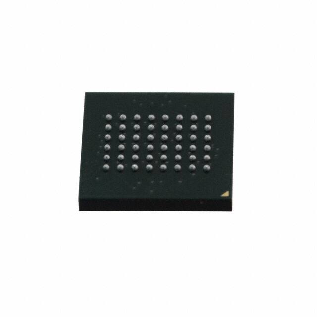
The MR256D08B is available in small footprint 8 mm x 8 mm, 48-pin ball grid array (BGA) package with
0.75 mm ball centers.
The MR256D08B provides highly reliable data storage over a wide range of temperatures. The product is
offered with commercial temperature (0 to +70 °C).
CONTENTS
1. DEVICE PIN ASSIGNMENT......................................................................... 2
2. ELECTRICAL SPECIFICATIONS................................................................. 4
3. TIMING SPECIFICATIONS.......................................................................... 8
4. ORDERING INFORMATION....................................................................... 13
5. MECHANICAL DRAWING.......................................................................... 14
6. REVISION HISTORY...................................................................................... 15
How to Reach Us.......................................................................................... 15
Copyright © 2018 Everspin Technologies, Inc.
1
MR256D08B Rev. 3.3 3/2018
�MR256D08B
1. DEVICE PIN ASSIGNMENT
Figure 1.1 Block Diagram
OUTPUT
ENABLE
BUFFER
G
A[14:0]
15
OUTPUT ENABLE
7
ADDRESS
BUFFER
8
ROW
DECODER
COLUMN
DECODER
CHIP
ENABLE
BUFFER
E
8
8
OUTPUT
BUFFER
8
32K x 8 BIT
MEMORY
ARRAY
WRITE
ENABLE
BUFFER
W
SENSE
AMPS
8
FINAL
WRITE
DRIVERS
8
WRITE
DRIVER
8
DQ[7:0]
WRITE ENABLE
Table 1.1 Pin Functions
Signal Name
Function
A
Address Input
E
Chip Enable
W
Write Enable
G
Output Enable
DQ
Data I/O
VDD
Power Supply
VDDQ
I/O Power Supply
VSS
Ground
DC
Do Not Connect
NC
No Connection, Ball D3, H1, H6, G2 Reserved for Future Expansion
Copyright © 2018 Everspin Technologies, Inc.
2
MR256D08B Rev. 3.3 3/2018
�MR256D08B
DEVICE PIN ASSIGNMENT
Figure 1.2 Pin Diagrams for Available Packages (Top View)
1
2
3
4
5
6
DC
G
A
A
A
VDD
A
NC
DC
A
A
E
DC
B
DQ
VDD
A
A
NC
DQ
C
VSS
DQ
NC
A
DQ
VDDQ
D
VDDQ
DQ
DC
VSS
DQ
VSS
E
DQ3
NC
VSS
NC
DQ
F
NC
NC
A
A
W
NC
G
NC
A
A
A
A
NC
H
48 Pin FBGA
Table 1.2 Operating Modes
E1
G1
W1
Mode
VDD Current
DQ[7:0]2
H
X
X
Not selected
ISB1, ISB2
Hi-Z
L
H
H
Output disabled
IDDR
Hi-Z
L
L
H
Byte Read
IDDR
DOut
L
X
L
Byte Write
IDDW
Din
1
H = high, L = low, X = don’t care
2
Hi-Z = high impedance
Copyright © 2018 Everspin Technologies, Inc.
3
MR256D08B Rev. 3.3 3/2018
�MR256D08B
2. ELECTRICAL SPECIFICATIONS
Absolute Maximum Ratings
This device contains circuitry to protect the inputs against damage caused by high static voltages or
electric fields; however, it is advised that normal precautions be taken to avoid application of any
voltage greater than maximum rated voltages to these high-impedance (Hi-Z) circuits.
The device also contains protection against external magnetic fields. Precautions should be taken
to avoid application of any magnetic field more intense than the maximum field intensity specified
in the maximum ratings.
Table 2.1 Absolute Maximum Ratings1
Parameter
Symbol
Value
Unit
Core Supply voltage2
VDD
-0.5 to 4.0
V
I/O Power Supply voltage2
VDDQ
-0.5 to 4.0
V
-0.5 to +4.0 or
Voltage on any pin2
VIN
VDDQ + 0.5
V
whichever is less
Output current per pin
IOUT
±20
mA
Package power dissipation 3
PD
0.600
W
Temperature under bias
TBIAS
-10 to 85
°C
Storage Temperature
Tstg
-55 to 150
°C
Lead temperature during solder (3 minute max)
TLead
260
°C
Maximum magnetic field during write
Hmax_write
2000
A/m
Maximum magnetic field during read or standby
Hmax_read
8000
A/m
1
Permanent device damage may occur if absolute maximum ratings are exceeded. Functional operation should be restricted to recommended operating conditions. Exposure to excessive voltages or
magnetic fields could affect device reliability.
2
All voltages are referenced to VSS.
Power dissipation capability depends on package characteristics and use environment.
3
Copyright © 2018 Everspin Technologies, Inc.
4
MR256D08B Rev. 3.3 3/2018
�MR256D08B
Electrical Specifications
Table 2.2 Operating Conditions
Parameter
Symbol
Min
Typical
Max
Unit
Core Power supply voltage
VDD
3.0
3.3
3.6
V
I/O Power supply voltage
VDDQ
1.65i
-
3.6
V
Write inhibit voltage
VWIDD
2.5
2.7
3.0 i
V
Write inhibit voltage
VWIDDQ
1.2
1.4
1.65i
V
Input high voltage (VDDQ=1.65-2.2V)
VIH
1.4
-
VDDQ + 0.2 ii
V
Input high voltage (VDDQ=2.2-2.7V)
VIH
1.8
-
VDDQ + 0.2 ii
V
Input high voltage (VDDQ=2.7-3.6V)
VIH
2.2
-
VDDQ + 0.2 ii
V
Input low voltage (VDDQ=1.65-2.2V)
VIL
-0.2 iii
-
0.4
V
Input low voltage (VDDQ=2.2-2.7V)
VIL
-0.2 iii
-
0.6
V
Input low voltage (VDDQ=2.7-3.6V)
VIL
-0.2 iii
-
0.8
V
Temperature under bias
TA
0
70
°C
i
VDDQ≤VDD. Write inhibit occurs when either VDD or VDDQ drops below its write inhibit voltage. There is a 2 ms startup time once
VDD exceeds VDD(min). See Power Up and Power Down Sequencing.
ii
VIH(max) = VDDQ + 0.2 V DC ; VIH(max) = VDDQ + 0.5 V AC (pulse width ≤ 20 ns) for I ≤ 20.0 mA.
iii
VIL(min) = -0.2 V DC ; VIL(min) = -2.0 V AC (pulse width ≤ 20 ns) for I ≤ 20.0 mA.
i
Copyright © 2018 Everspin Technologies, Inc.
5
MR256D08B Rev. 3.3 3/2018
�MR256D08B
Electrical Specifications
Power Up and Power Down Sequencing
MRAM is protected from write operations whenever VDD is less than VWIDD or VDDQ is less than VWIDDQ. As soon
as VDD exceeds VDD(min) and VDDQ exceeds VDDQ(min), there is a startup time of 2 ms before read or write operations can start. This time allows memory power supplies to stabilize.
The E and W control signals should track VDD on power up to VDD- 0.2 V or VIH (whichever is lower) and remain
high for the startup time. In most systems, this means that these signals should be pulled up with a resistor so that signal remains high if the driving signal is Hi-Z during power up. Any logic that drives E and W
should hold the signals high with a power-on reset signal for longer than the startup time.
During power loss or brownout where either VDD goes below VWIDD or VDDQ goes below VWIDDQ, writes are protected and a startup time must be observed when power returns above VDD(min) and / or VDDQ.
Figure 2.1 Power Up and Power Down Diagram
VWIDD VDD / VDDQ
VWIDDQ
STARTUP
2 ms
READ/WRITE
INHIBITED
BROWNOUT or POWER LOSS
NORMAL
OPERATION
READ/WRITE
INHIBITED
2 ms
RECOVER
NORMAL
OPERATION
VIH
VIH
E
W
Copyright © 2018 Everspin Technologies, Inc.
6
MR256D08B Rev. 3.3 3/2018
�MR256D08B
Electrical Specifications
Table 2.3 DC Characteristics
Parameter
Symbol
Min
Typical
Max
Unit
Input leakage current
Ilkg(I)
-
-
±1
μA
Output leakage current
Ilkg(O)
-
-
±1
μA
Output low voltage (VDDQ=1.65-2.2V@ 0.1mA)
VOL
-
-
0.2
V
Output low voltage (VDDQ=2.2-2.7V@ 0.1mA)
VOL
-
-
0.4
V
Output low voltage (VDDQ=2.7-3.6V@ 2.1 mA)
VOL
-
-
0.4
V
Output high voltage (VDDQ=1.65-2.2V@ - 0.1 mA)
VOH
1.4
-
-
V
Output high voltage (VDDQ=2.2-2.7V@ -0.1 mA)
VOH
2
-
-
V
Output high voltage (VDDQ=2.7-3.6V@ -1.0 mA)
VOH
2.4
-
-
V
Table 2.4 Power Supply Characteristics
Parameter
AC active supply current - read modes1
(IOUT= 0 mA, VDD= max)
AC active supply current - write modes1
(VDD= max)
Symbol
Typical
Max
Unit
IDDR
25
30
mA
IDDW
55
65
mA
IDDQ
0.50
2
mA
ISB1
6
8
mA
ISB2
5
7
mA
AC active operating current
(VDDQ = VIH= 3.6V, VIL= 0V)
input transitions
很抱歉,暂时无法提供与“MR256D08BMA45R”相匹配的价格&库存,您可以联系我们找货
免费人工找货