Important notice
Dear Customer,
On 7 February 2017 the former NXP Standard Product business became a new company with the
tradename Nexperia. Nexperia is an industry leading supplier of Discrete, Logic and PowerMOS
semiconductors with its focus on the automotive, industrial, computing, consumer and wearable
application markets
In data sheets and application notes which still contain NXP or Philips Semiconductors references, use
the references to Nexperia, as shown below.
Instead of http://www.nxp.com, http://www.philips.com/ or http://www.semiconductors.philips.com/,
use http://www.nexperia.com
Instead of sales.addresses@www.nxp.com or sales.addresses@www.semiconductors.philips.com, use
salesaddresses@nexperia.com (email)
Replace the copyright notice at the bottom of each page or elsewhere in the document, depending on
the version, as shown below:
- © NXP N.V. (year). All rights reserved or © Koninklijke Philips Electronics N.V. (year). All rights
reserved
Should be replaced with:
- © Nexperia B.V. (year). All rights reserved.
If you have any questions related to the data sheet, please contact our nearest sales office via e-mail
or telephone (details via salesaddresses@nexperia.com). Thank you for your cooperation and
understanding,
Kind regards,
Team Nexperia
�CBT16292
12-bit 1-of-2 multiplexer/demultiplexer
Rev. 02 — 18 April 2008
Product data sheet
1. General description
The CBT16292 is a 12-bit 1-of-2 high-speed TTL-compatible multiplexer/demultiplexer.
The low ON resistance of the switch allows connections to be made with minimal
propagation delay.
When the select input (S) is LOW, port nA is connected to port nB1 and port nB2 is
connected to GND via an internal pull-down resistor (500 Ω). When select input (S) is
HIGH, port nA is connected to port nB2 and nB1 is connected to GND via an internal
pull-down resistor (500 Ω).
The CBT16292 is characterized for operation from –40 °C to +85 °C.
2. Features
6 Ω switch connection between two ports
TTL compatible input levels
Break-before-make feature
Internal 500 Ω pull-down resistors to ground
ESD protection:
u HBM JESD22-A114E Class 2 exceeds 2000 V
u MM JESD22-A115-A exceeds 200 V
u CDM JESD22-C101C exceeds 1000 V
n Latch-up performance exceeds 500 mA per JESD 78
n
n
n
n
n
3. Ordering information
Table 1.
Ordering information
Type number
CBT16292DGG
Package
Temperature range Name
Description
Version
−40 °C to 85 °C
plastic thin shrink small outline package; 56 leads;
body width 6.1 mm
SOT364-1
TSSOP56
�CBT16292
NXP Semiconductors
12-bit 1-of-2 multiplexer/demultiplexer
4. Functional diagram
2
4
6
9
11
13
15
18
21
23
25
27
1
1A
2A
3A
4A
5A
6A
7A
8A
9A
10A
11A
12A
1B1
1B2
2B1
2B2
3B1
3B2
4B1
4B2
5B1
5B2
6B1
6B2
7B1
7B2
8B1
8B2
9B1
9B2
10B1
10B2
11B1
11B2
12B1
12B2
54
53
52
51
50
1A
48
1B1
46
500 Ω
45
44
53
43
1B2
42
41
40
39
37
36
12A
27
30
12B1
35
500 Ω
34
33
500 Ω
32
31
29
30
12B2
29
S
Logic symbol
S
Fig 2.
1
001aah984
Logic diagram
CBT16292_2
Product data sheet
54
500 Ω
47
001aah983
Fig 1.
2
© NXP B.V. 2008. All rights reserved.
Rev. 02 — 18 April 2008
2 of 11
�CBT16292
NXP Semiconductors
12-bit 1-of-2 multiplexer/demultiplexer
5. Pinning information
5.1 Pinning
S
1
56 n.c.
1A
2
55 n.c.
n.c.
3
54 1B1
2A
4
53 1B2
n.c.
5
52 2B1
3A
6
51 2B2
n.c.
7
50 3B1
GND
8
49 GND
4A
9
48 3B2
n.c. 10
47 4B1
5A 11
46 4B2
n.c. 12
45 5B1
6A 13
44 5B2
n.c. 14
43 6B1
CBT16292
7A 15
42 6B2
n.c. 16
41 7B1
VCC 17
40 7B2
8A 18
39 8B1
GND 19
38 GND
n.c. 20
37 8B2
9A 21
36 9B1
n.c. 22
35 9B2
10A 23
34 10B1
n.c. 24
33 10B2
11A 25
32 11B1
n.c. 26
31 11B2
12A 27
30 12B1
n.c. 28
29 12B2
001aah985
Fig 3.
Pin configuration SOT364-1 (TSSOP56)
5.2 Pin description
Table 2.
Pin description
Symbol
Pin
Description
S
1
select input
nA
2, 4, 6, 9, 11, 13, 15, 18, 21, 23, 25, 27
common input or output (1A to 12A)
n.c.
3, 5, 7, 10, 12, 14, 16, 20, 22, 24, 26, 28, 55, 56
not connected
GND
8, 19, 38, 49
ground (0 V)
VCC
17
supply voltage
nB1
54, 52, 50, 47, 45, 43, 41, 39, 36, 34, 32, 30
independent input or output (1B1 to 12B1)
nB2
53, 51, 48, 46, 44, 42, 40, 37, 35, 33, 31, 29
independent input or output (1B2 to 12B2)
CBT16292_2
Product data sheet
© NXP B.V. 2008. All rights reserved.
Rev. 02 — 18 April 2008
3 of 11
�CBT16292
NXP Semiconductors
12-bit 1-of-2 multiplexer/demultiplexer
6. Functional description
Table 3.
Function selection[1]
S input
Channel on
L
nA to nB1 or nB1 to nA
(nB2 connected to GND via internal resistor (500 Ω)
H
nA to nB2 or nB2 to nA
(nB1 connected to GND via internal resistor (500 Ω)
[1]
H = HIGH voltage level; L = LOW voltage level.
7. Limiting values
Table 4.
Limiting values [1][2]
In accordance with the Absolute Maximum Rating System (IEC 60134).
Symbol
Parameter
VCC
supply voltage
Conditions
Min
Max
Unit
−0.5
+7.0
V
VI
input voltage
−0.5
+7.0
V
IIK
input clamping current
VI < 0 V
−50
-
mA
ISW
switch current
continuous current through channel
−128
+128
mA
Tstg
storage temperature
−65
+150
°C
-
600
mW
total power dissipation
Ptot
[3]
Tamb = −40 °C to +125 °C
[4]
[1]
Stresses beyond those listed may cause permanent damage to the device. These are stress ratings only and functional operation of the
device at these or any other conditions beyond those indicated under “recommended operating conditions” is not implied. Exposure to
absolute-maximum-rated conditions for extended periods may affect device reliability.
[2]
The performance capability of a high-performance integrated circuit in conjunction with its thermal environment can create junction
temperatures which are detrimental to reliability. The maximum junction temperature of this integrated circuit should not exceed 150 °C.
[3]
The input and output negative voltage ratings may be exceeded if the input and output clamp current ratings are observed.
[4]
Ptot derates linearly with 8 mW/K above 55 °C.
8. Recommended operating conditions
Table 5.
Operating conditions
All unused control inputs of the device must be held at VCC or GND to ensure proper device operation.
Symbol
Parameter
VCC
Conditions
Min
Max
Unit
supply voltage
4.0
5.5
V
VIH
HIGH-level input voltage
2.0
-
V
VIL
LOW-level input voltage
-
0.8
V
Tamb
ambient temperature
−40
+85
°C
operating in free-air
CBT16292_2
Product data sheet
© NXP B.V. 2008. All rights reserved.
Rev. 02 — 18 April 2008
4 of 11
�CBT16292
NXP Semiconductors
12-bit 1-of-2 multiplexer/demultiplexer
9. Static characteristics
Table 6.
Static characteristics
Tamb = −40 °C to +85 °C.
Symbol
Parameter
Conditions
VIK
input clamping voltage
VCC = 4.5 V; II = −18 mA
Min
Typ[1]
Max
Unit
-
-
−1.2
V
II
input leakage current
VCC = 5.5 V; VI = VCC or GND
-
-
±5
µA
ICC
supply current
VCC = 5.5 V; IO = 0 mA;
VI = VCC or GND
-
-
3
µA
∆ICC
additional supply current
per input; VCC = 5.5 V; one input at
3.4 V, other inputs at VCC or GND
-
-
2.5
mA
CI
input capacitance
select input S; VCC = 5.0 V;
VI = 3 V or 0 V
-
4
-
pF
Cio(off)
off-state input/output capacitance
VO = 3 V or 0 V; VCC = 0 V
-
6
-
pF
VI = 0 V; II = 64 mA
-
8
12.5
Ω
VI = 0 V; II = 30 mA
-
8
11
Ω
VI = 2.4 V; II = 15 mA
-
13
16
Ω
RON
ON resistance
[2]
[3]
VCC = 4.5 V
[1]
All typical values are measured at Tamb = 25 °C.
[2]
This is the increase in supply current for each input that is at the specified TTL voltage level rather than VCC or GND.
[3]
Measured by the voltage drop between the A and the B terminals at the indicated current through the switch. ON resistance is
determined by the lowest voltage of the two (A or B) terminals.
10. Dynamic characteristics
Table 7.
Dynamic characteristics
Tamb = −40 °C to +85 °C; VCC = 5.0 V ± 0.5 V; for test circuit see Figure 6.
Symbol
Parameter
propagation delay
tpd
Conditions
nA, nBn to nBn, nA; see Figure 4
[1][2]
Min
Typ
Max
Unit
-
-
0.4
ns
ten
enable time
S to nA, nBn; see Figure 5
[2]
1.5
-
6.0
ns
tdis
disable time
S to nA, nBn; see Figure 5
[2]
2.2
-
5.5
ns
nA, nBn to nBn, nA
[3]
0
-
2.0
ns
break-before-make time
tb-m
[1]
This parameter is warranted but not production tested. The propagation delay is based on the RC time constant of the typical
ON resistance of the switch and a load capacitance, when driven by an ideal voltage source (zero output impedance).
[2]
tpd is the same as tPLH and tPHL.
ten is the same as tPZL and tPZH.
tdis is the same as tPLZ and tPHZ.
[3]
Time interval between break and make measured at the same operating point (VCC and temperature).
CBT16292_2
Product data sheet
© NXP B.V. 2008. All rights reserved.
Rev. 02 — 18 April 2008
5 of 11
�CBT16292
NXP Semiconductors
12-bit 1-of-2 multiplexer/demultiplexer
11. Waveforms
VI
input
GND
VM
VM
tPLH
tPHL
VOH
output
VM
VM
VOL
001aah986
Measurement points are given in Table 8.
VOL and VOH are typical output voltage levels that occur with the output load.
Fig 4.
Input (nA or nBn) to output (nBn or nA) propagation delays
VI
S input
GND
3.5 V
output
OFF to LOW
LOW to OFF V
OL
output
OFF to HIGH
HIGH to OFF
VM
VM
tPZL
tPLZ
VM
VOL + 0.3 V
tPZH
tPHZ
VOH
VOH − 0.3 V
VM
GND
001aah987
Measurement points are given in Table 8.
VOL and VOH are typical output voltage levels that occur with the output load.
Fig 5.
Table 8.
Enable and disable times
Measurement points
Supply voltage
Input
Output
VCC
VM
VI
VM
4.5 V to 5.5 V
1.5 V
GND to 3.0 V
1.5 V
CBT16292_2
Product data sheet
© NXP B.V. 2008. All rights reserved.
Rev. 02 — 18 April 2008
6 of 11
�CBT16292
NXP Semiconductors
12-bit 1-of-2 multiplexer/demultiplexer
VEXT
VCC
VI
RL
VO
G
DUT
RT
CL
RL
mna616
Test data is given in Table 9.
Definitions for test circuit:
RL = Load resistance.
CL = Load capacitance including jig and probe capacitance.
RT = Termination resistance should be equal to the output impedance Zo of the pulse generator.
VEXT = External voltage for measuring switching times.
Fig 6.
Test circuit
Table 9.
Test data
Supply voltage
Input
Load
VEXT
VCC
VI
tr = tf
CL
RL
tPLH, tPHL
tPZH, tPHZ
tPZL, tPLZ
4.5 V to 5.5 V
GND to 3.0 V
≤ 2.5 ns
50 pF
500 Ω
open
open
7.0 V
CBT16292_2
Product data sheet
© NXP B.V. 2008. All rights reserved.
Rev. 02 — 18 April 2008
7 of 11
�CBT16292
NXP Semiconductors
12-bit 1-of-2 multiplexer/demultiplexer
12. Package outline
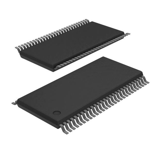
TSSOP56: plastic thin shrink small outline package; 56 leads; body width 6.1 mm
SOT364-1
E
D
A
X
c
HE
y
v M A
Z
56
29
Q
A2
(A 3)
A1
pin 1 index
A
θ
Lp
L
1
detail X
28
w M
bp
e
2.5
0
5 mm
scale
DIMENSIONS (mm are the original dimensions).
UNIT
A
max.
A1
A2
A3
bp
c
D (1)
E (2)
e
HE
L
Lp
Q
v
w
y
Z
θ
mm
1.2
0.15
0.05
1.05
0.85
0.25
0.28
0.17
0.2
0.1
14.1
13.9
6.2
6.0
0.5
8.3
7.9
1
0.8
0.4
0.50
0.35
0.25
0.08
0.1
0.5
0.1
8
o
0
o
Notes
1. Plastic or metal protrusions of 0.15 mm maximum per side are not included.
2. Plastic interlead protrusions of 0.25 mm maximum per side are not included.
OUTLINE
VERSION
SOT364-1
Fig 7.
REFERENCES
IEC
JEDEC
JEITA
EUROPEAN
PROJECTION
ISSUE DATE
99-12-27
03-02-19
MO-153
Package outline SOT364-1 (TSSOP56)
CBT16292_2
Product data sheet
© NXP B.V. 2008. All rights reserved.
Rev. 02 — 18 April 2008
8 of 11
�CBT16292
NXP Semiconductors
12-bit 1-of-2 multiplexer/demultiplexer
13. Abbreviations
Table 10.
Abbreviations
Acronym
Description
CDM
Charged Device Model
DUT
Device Under Test
ESD
ElectroStatic Discharge
HBM
Human Body Model
MM
Machine Model
TTL
Transistor-Transistor Logic
14. Revision history
Table 11.
Revision history
Document ID
Release date
Data sheet status
Change notice
Supersedes
CBT16292_2
20080418
Product data sheet
-
CBT16292_1
Modifications:
CBT16292_1
•
The format of this data sheet has been redesigned to comply with the new identity
guidelines of NXP Semiconductors.
•
•
Legal texts have been adapted to the new company name where appropriate.
Changed ten from 5.8 ns to 6.0 ns in Table 7 “Dynamic characteristics”.
19990913
Product specification
CBT16292_2
Product data sheet
-
-
© NXP B.V. 2008. All rights reserved.
Rev. 02 — 18 April 2008
9 of 11
�CBT16292
NXP Semiconductors
12-bit 1-of-2 multiplexer/demultiplexer
15. Legal information
15.1 Data sheet status
Document status[1][2]
Product status[3]
Definition
Objective [short] data sheet
Development
This document contains data from the objective specification for product development.
Preliminary [short] data sheet
Qualification
This document contains data from the preliminary specification.
Product [short] data sheet
Production
This document contains the product specification.
[1]
Please consult the most recently issued document before initiating or completing a design.
[2]
The term ‘short data sheet’ is explained in section “Definitions”.
[3]
The product status of device(s) described in this document may have changed since this document was published and may differ in case of multiple devices. The latest product status
information is available on the Internet at URL http://www.nxp.com.
15.2 Definitions
Draft — The document is a draft version only. The content is still under
internal review and subject to formal approval, which may result in
modifications or additions. NXP Semiconductors does not give any
representations or warranties as to the accuracy or completeness of
information included herein and shall have no liability for the consequences of
use of such information.
Short data sheet — A short data sheet is an extract from a full data sheet
with the same product type number(s) and title. A short data sheet is intended
for quick reference only and should not be relied upon to contain detailed and
full information. For detailed and full information see the relevant full data
sheet, which is available on request via the local NXP Semiconductors sales
office. In case of any inconsistency or conflict with the short data sheet, the
full data sheet shall prevail.
15.3 Disclaimers
General — Information in this document is believed to be accurate and
reliable. However, NXP Semiconductors does not give any representations or
warranties, expressed or implied, as to the accuracy or completeness of such
information and shall have no liability for the consequences of use of such
information.
Right to make changes — NXP Semiconductors reserves the right to make
changes to information published in this document, including without
limitation specifications and product descriptions, at any time and without
notice. This document supersedes and replaces all information supplied prior
to the publication hereof.
Suitability for use — NXP Semiconductors products are not designed,
authorized or warranted to be suitable for use in medical, military, aircraft,
space or life support equipment, nor in applications where failure or
malfunction of an NXP Semiconductors product can reasonably be expected
to result in personal injury, death or severe property or environmental
damage. NXP Semiconductors accepts no liability for inclusion and/or use of
NXP Semiconductors products in such equipment or applications and
therefore such inclusion and/or use is at the customer’s own risk.
Applications — Applications that are described herein for any of these
products are for illustrative purposes only. NXP Semiconductors makes no
representation or warranty that such applications will be suitable for the
specified use without further testing or modification.
Limiting values — Stress above one or more limiting values (as defined in
the Absolute Maximum Ratings System of IEC 60134) may cause permanent
damage to the device. Limiting values are stress ratings only and operation of
the device at these or any other conditions above those given in the
Characteristics sections of this document is not implied. Exposure to limiting
values for extended periods may affect device reliability.
Terms and conditions of sale — NXP Semiconductors products are sold
subject to the general terms and conditions of commercial sale, as published
at http://www.nxp.com/profile/terms, including those pertaining to warranty,
intellectual property rights infringement and limitation of liability, unless
explicitly otherwise agreed to in writing by NXP Semiconductors. In case of
any inconsistency or conflict between information in this document and such
terms and conditions, the latter will prevail.
No offer to sell or license — Nothing in this document may be interpreted
or construed as an offer to sell products that is open for acceptance or the
grant, conveyance or implication of any license under any copyrights, patents
or other industrial or intellectual property rights.
Quick reference data — The Quick reference data is an extract of the
product data given in the Limiting values and Characteristics sections of this
document, and as such is not complete, exhaustive or legally binding.
15.4 Trademarks
Notice: All referenced brands, product names, service names and trademarks
are the property of their respective owners.
16. Contact information
For more information, please visit: http://www.nxp.com
For sales office addresses, please send an email to: salesaddresses@nxp.com
CBT16292_2
Product data sheet
© NXP B.V. 2008. All rights reserved.
Rev. 02 — 18 April 2008
10 of 11
�CBT16292
NXP Semiconductors
12-bit 1-of-2 multiplexer/demultiplexer
17. Contents
1
2
3
4
5
5.1
5.2
6
7
8
9
10
11
12
13
14
15
15.1
15.2
15.3
15.4
16
17
General description . . . . . . . . . . . . . . . . . . . . . . 1
Features . . . . . . . . . . . . . . . . . . . . . . . . . . . . . . . 1
Ordering information . . . . . . . . . . . . . . . . . . . . . 1
Functional diagram . . . . . . . . . . . . . . . . . . . . . . 2
Pinning information . . . . . . . . . . . . . . . . . . . . . . 3
Pinning . . . . . . . . . . . . . . . . . . . . . . . . . . . . . . . 3
Pin description . . . . . . . . . . . . . . . . . . . . . . . . . 3
Functional description . . . . . . . . . . . . . . . . . . . 4
Limiting values. . . . . . . . . . . . . . . . . . . . . . . . . . 4
Recommended operating conditions. . . . . . . . 4
Static characteristics. . . . . . . . . . . . . . . . . . . . . 5
Dynamic characteristics . . . . . . . . . . . . . . . . . . 5
Waveforms . . . . . . . . . . . . . . . . . . . . . . . . . . . . . 6
Package outline . . . . . . . . . . . . . . . . . . . . . . . . . 8
Abbreviations . . . . . . . . . . . . . . . . . . . . . . . . . . . 9
Revision history . . . . . . . . . . . . . . . . . . . . . . . . . 9
Legal information. . . . . . . . . . . . . . . . . . . . . . . 10
Data sheet status . . . . . . . . . . . . . . . . . . . . . . 10
Definitions . . . . . . . . . . . . . . . . . . . . . . . . . . . . 10
Disclaimers . . . . . . . . . . . . . . . . . . . . . . . . . . . 10
Trademarks . . . . . . . . . . . . . . . . . . . . . . . . . . . 10
Contact information. . . . . . . . . . . . . . . . . . . . . 10
Contents . . . . . . . . . . . . . . . . . . . . . . . . . . . . . . 11
Please be aware that important notices concerning this document and the product(s)
described herein, have been included in section ‘Legal information’.
© NXP B.V. 2008.
All rights reserved.
For more information, please visit: http://www.nxp.com
For sales office addresses, please send an email to: salesaddresses@nxp.com
Date of release: 18 April 2008
Document identifier: CBT16292_2
�