Important notice
Dear Customer,
On 7 February 2017 the former NXP Standard Product business became a new company with the
tradename Nexperia. Nexperia is an industry leading supplier of Discrete, Logic and PowerMOS
semiconductors with its focus on the automotive, industrial, computing, consumer and wearable
application markets
In data sheets and application notes which still contain NXP or Philips Semiconductors references, use
the references to Nexperia, as shown below.
Instead of http://www.nxp.com, http://www.philips.com/ or http://www.semiconductors.philips.com/,
use http://www.nexperia.com
Instead of sales.addresses@www.nxp.com or sales.addresses@www.semiconductors.philips.com, use
salesaddresses@nexperia.com (email)
Replace the copyright notice at the bottom of each page or elsewhere in the document, depending on
the version, as shown below:
- © NXP N.V. (year). All rights reserved or © Koninklijke Philips Electronics N.V. (year). All rights
reserved
Should be replaced with:
- © Nexperia B.V. (year). All rights reserved.
If you have any questions related to the data sheet, please contact our nearest sales office via e-mail
or telephone (details via salesaddresses@nexperia.com). Thank you for your cooperation and
understanding,
Kind regards,
Team Nexperia
�INTEGRATED CIRCUITS
74ALVCH16823
18-bit bus-interface D-type flip-flop
with reset and enable (3-State)
Product specification
IC24 Data Handbook
�������
�� ���
�����
�
1998 Jul 29
�Philips Semiconductors
Product specification
18-bit D-type flip-flop (3-State)
74ALVCH16823
FEATURES
DESCRIPTION
• Wide supply voltage range of 1.2V to 3.6V
• Complies with JEDEC standard no. 8-1A.
• CMOS low power consumption
• Direct interface with TTL levels
• Current drive ± 24 mA at 3.0 V
• Multibyteflow-through standard pin-out architecture
• Low inductance multiple VCC and GND pins to minimize noise and
The 74ALVCH16823 is a 18-bit edge-triggered flip-flop featuring
separate D-type inputs for each flip-flop and 3-state outputs for bus
oriented applications. Incorporates bushold data inputs which
eliminate the need for external pull-up resistors to hold unused
inputs. The74ALVCH16823 consists of two sections of nine
edge-triggered flip-flops. A clock (CP) input, an output-enable (OE)
input, a Master reset (MR) input and a clock-enable( CE) input are
provided for each total 9-bit section.
With the clock-enable (CE) input LOW, the D-type flip-flops will store
the state of their individual D-inputs that meet the set-up and hold
time requirements on the LOW-to-HIGH CP transition. Taking CE
HIGH disables the clock buffer, thus latching the outputs. Taking the
Master reset (MR) input LOW causes all the Q outputs to go LOW
independently of the clock.
ground bounce
• All data inputs have bus hold
• Output drive capability 50Ω transmission lines @ 85°C
When OE is LOW, the contents of the flip-flops are available at the
outputs. When the OE is HIGH, the outputs go to the high
impedance OFF-state. Operation of the OE input does not affect the
state of flip-flops.
Active bus hold circuitry is provided to hold unused or floating data
inputs at a valid logic level.
QUICK REFERENCE DATA
GND = 0V; Tamb = 25°C; tr = tf ≤ 2.5ns
TYPICAL
UNIT
tPHL/tPLH
Propagation delay
CP to Qn
PARAMETER
VCC = 2.5V, CL = 30pF
VCC = 3.3V, CL = 50pF
2.1
2.1
ns
Fmax
Maximum clock frequency
VCC = 2.5V, CL = 30pF
VCC = 3.3V, CL = 50pF
300
350
MHz
CI
Input capacitance
5.0
pF
CPD
Power dissipation capacitance per latch
SYMBOL
CONDITIONS
VI = GND to VCC1
Outputs enabled
16
Outputs disabled
10
pF
NOTES:
1. CPD is used to determine the dynamic power dissipation (PD in �W):
PD = CPD × VCC2 × fi + � (CL × VCC2 × fo) where:
fi = input frequency in MHz; CL = output load capacity in pF;
fo = output frequency in MHz; VCC = supply voltage in V;
� (CL × VCC2 × fo) = sum of outputs.
ORDERING INFORMATION
PACKAGES
TEMPERATURE RANGE
OUTSIDE NORTH AMERICA
NORTH AMERICA
DWG NUMBER
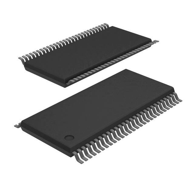
56-Pin Plastic SSOP Type II
-40°C to +85°C
74ALVCH16823 DL
ACH16823 DL
SOT371-1
56-Pin Plastic TSSOP Type II
-40°C to +85°C
74ALVCH16823 DGG
ACH16823 DGG
SOT364-1
1998 Jul 29
2
853–2100 19800
�Philips Semiconductors
Product specification
18-bit D-type flip-flop (3-State)
74ALVCH16823
PIN DESCRIPTION
PIN NUMBER
SYMBOL
2, 27
1OE, 2OE
Output enable input (active-Low)
FUNCTION
54, 52, 51, 49, 48, 47, 45, 44, 43
42, 41, 40, 38, 37, 36, 34, 33, 31
1D0-1D8
2D0-2D8
Data inputs
3, 5, 6, 8, 9, 10, 12, 13, 14
15, 16, 17, 19, 20, 21, 23, 24, 26
1Q0-1Q8
2Q0-2Q8
Data outputs
56, 29
1CP, 2CP
Clock pulse input (active rising edge)
55, 30
1CE, 2CE
Clock enable input (active-Low)
1, 28
1MR, 2MR
Master reset input (active-Low)
4, 11, 18, 25, 32, 39, 46, 53
GND
Ground (0V)
7, 22, 35, 50
VCC
Positive supply voltage
PIN CONFIGURATION
LOGIC SYMBOL
1
1MR
1
56
1CP
1OE
2
55
1CE
1Q0
3
54
1D0
GND
4
53
GND
1Q1
5
52
1D1
1Q2
6
51
1D2
VCC
7
50
VCC
1Q3
8
49
1D3
1Q4
9
48
1D4
1Q5
10
47
1D5
GND
11
46
GND
1Q6
12
45
1D6
1Q7
13
44
1D7
1Q8
14
43
1D8
2Q0
15
42
2D0
2Q1
16
41
2D1
2Q2
17
40
2D2
GND
18
39
GND
2Q3
19
38
2D3
2Q4
20
37
2D4
2Q5
21
36
2D5
VCC
22
35
VCC
2Q6
23
34
2D6
2Q7
24
33
2D7
GND
25
32
GND
2Q8
26
31
2D8
2OE
27
30
2CE
2MR
28
29
2CP
28
2
27
1MR 2MR 1OE 2OE
54
52
51
49
48
47
45
44
43
42
41
40
38
37
36
34
33
31
A0
A1
A2
A3
B0
B1
B2
B3
A4
A5
A6
A7
B4
B5
B6
B7
A8
A9
A10
A11
B8
B9
B10
B11
A12
A13
A14
A15
B12
B13
B14
B15
A16
A17
B16
B17
3
5
6
8
9
10
12
13
14
15
16
17
19
20
21
23
24
26
1CP 2CP 1CE 2CE
48
29
55
30
SW00341
SH00014
1998 Jul 29
3
�Philips Semiconductors
Product specification
18-bit D-type flip-flop (3-State)
74ALVCH16823
LOGIC SYMBOL (IEEE/IEC)
BUS HOLD CIRCUIT
VCC
2
EN1
1MR
1
R2
1CE
55
G3
1CP
56
2OE
27
EN5
2MR
28
R6
2CE
30
G7
2CP
29
1D0
54
3
1Q0
1D1
52
5
1Q1
1D2
51
6
1Q2
1D3
49
8
1Q3
1D4
48
9
1Q4
1D5
47
10
1Q5
1D6
45
12
1Q6
1D7
44
13
1Q7
1D8
43
14
1Q8
15
2Q0
1OE
2D0
3C4
Data Input
To internal circuit
7C8
1, 2 ∇
4D
42
5, 6 ∇
8D
2D1
41
16
2Q1
2D2
40
17
2Q2
2D3
38
19
2Q3
2D4
37
20
2Q4
2D5
36
21
2Q5
2D6
34
23
2Q6
2D7
33
24
2Q7
2D8
31
25
2Q8
SW00044
SH00015
LOGIC DIAGRAM
nCE
nD0
nD1
nD2
nD3
nD4
nD5
nD6
nD7
nD8
nCP
nD
R
CP
nD
R
Q
CP
nD
R
Q
CP
Q
CP
nD
nD
R
R
Q
CP
nD
R
Q
CP
nD
R
Q
CP
nD
R
Q
CP
nD
R
Q
CP
Q
nMR
nOE
nQ0
nQ1
nQ2
nQ3
nQ4
nQ5
nQ6
nQ7
nQ8
n = 1 or 2
SH00016
1998 Jul 29
4
�Philips Semiconductors
Product specification
18-bit D-type flip-flop (3-State)
74ALVCH16823
FUNCTION TABLE
INPUTS
H
h
L
l
X
Z
↑
OUTPUT
nOE
nMR
nCE
nCP
nDx
nQx
L
L
X
X
X
L
L
H
L
↑
h
H
L
H
L
↑
l
L
L
H
L
L
X
Q0
L
H
H
X
X
Q0
=
=
=
=
=
=
=
H
X
X
X
X
Z
HIGH voltage level
HIGH voltage level one set-up time prior to the Low-to-High clock transition
LOW voltage level
LOW voltage level one set-up time prior to the Low-to-High clock transition
Don’t care
HIGH impedance “off” state
LOW to High clock transition
OPERATING MODES
Clear
Load and read data
Hold
Disable outputs
RECOMMENDED OPERATING CONDITIONS
LIMITS
SYMBOL
VCC
VCC
PARAMETER
CONDITIONS
UNIT
MIN
MAX
DC supply voltage 2.5V range (for max. speed
performance @ 30 pF output load)
2.3
2.7
DC supply voltage 3.3V range (for max. speed
performance @ 50 pF output load)
3.0
3.6
V
DC supply voltage (for low-voltage applications)
VI
DC Input voltage range
VO
DC output voltage range
Tamb
Operating free-air temperature range
tr, tf
Input rise and fall times
1.2
3.6
V
for data input pins
0
VCC
V
for control pins
0
5.5
V
0
VCC
V
–40
+85
°C
0
0
20
10
ns/V
VCC = 2.3 to 3.0V
VCC = 3.0 to 3.6V
ABSOLUTE MAXIMUM RATINGS
In accordance with the Absolute Maximum Rating System (IEC 134). Voltages are referenced to GND (ground = 0V).
SYMBOL
VCC
PARAMETER
CONDITIONS
DC supply voltage
VI �0
IIK
DC input diode current
VI
DC in
input
ut voltage
IOK
DC output diode current
VO �VCC or VO � 0
VO
DC output voltage
Note 1
IO
DC output source or sink current
VO = 0 to VCC
For control pins1
IGND, ICC
Tstg
PTOT
For data
inputs1
DC VCC or GND current
Storage temperature range
Power dissipation per package
–plastic medium-shrink (SSOP)
–plastic thin-medium-shrink (TSSOP)
For temperature range: –40 to +125 °C
above +55°C derate linearly with 11.3 mW/K
above +55°C derate linearly with 8 mW/K
NOTE:
1. The input and output voltage ratings may be exceeded if the input and output current ratings are observed.
1998 Jul 29
5
RATING
UNIT
–0.5 to +4.6
V
–50
mA
–0.5 to +5.5
–0.5 to VCC +0.5
V
�50
mA
–0.5 to VCC +0.5
V
�50
mA
�100
mA
–65 to +150
°C
850
600
mW
�Philips Semiconductors
Product specification
18-bit D-type flip-flop (3-State)
74ALVCH16823
DC ELECTRICAL CHARACTERISTICS
Over recommended operating conditions. Voltage are referenced to GND (ground = 0 V).
LIMITS
SYMBOL
PARAMETER
TEST CONDITIONS
Temp = -40°C to +85°C
MIN
VIH
VIL
HIGH level Input
In ut voltage
LOW level In
Input
ut voltage
VCC = 1.2V
VCC
VCC = 1.8V
0.7*VCC
0.9
VCC = 2.3 to 2.7V
1.7
1.2
VCC = 2.7 to 3.6V
2.0
1.5
VOL
II
IIHZ/IILZ
IOZ
∆ICC
MAX
V
–
GND
VCC = 1.8V
0.9
0.2*VCC
VCC = 2.3 to 2.7V
1.2
0.7
1.5
0.8
VCC = 1
1.8
8 to 3
3.6V;
6V; VI = VIH or VIL; IO = –100µA
VCC�0.2
�0 2
VCC
–
VCC = 1.8V; VI = VIH or VIL; IO = –6mA
VCC�0.4
VCC�0.10
–
VCC = 2.3V; VI = VIH or VIL; IO = –6mA
VCC�0.3
VCC�0.08
–
VCC = 2.3V; VI = VIH or VIL; IO = –12mA
VCC�0.5
VCC�0.17
–
VCC = 2.3V; VI = VIH or VIL; IO = –18mA
VCC�0.6
VCC�0.26
–
VCC = 2.7V; VI = VIH or VIL; IO = –12mA
VCC�0.5
VCC�0.14
–
VCC = 3.0V; VI = VIH or VIL; IO = –24mA
VCC�1.0
VCC�0.28
–
8 to 3
6V; VI = VIH or VIL; IO = 100µA
VCC = 1
1.8
3.6V;
GND
0 20
0.20
VCC = 1.8V; VI = VIH or VIL; IO = 6mA
0.09
0.30
VCC = 2.3V; VI = VIH or VIL; IO = 6mA
0.07
0.20
VCC = 2.3V; VI = VIH or VIL; IO = 12mA
0.15
0.40
VCC = 2.3V; VI = VIH or VIL; IO = 18mA
0.23
0.60
VCC = 2.7V; VI = VIH or VIL; IO = 12mA
0.14
0.40
VCC = 3.0V; VI = VIH or VIL; IO = 24mA
0.27
0.55
Input leakage current per
control pin
VCC = 1.8 to 3.6V;
VI = 5.5V or GND
0.1
5
Input leakage current per data
pin
VCC = 1.8 to 3.6V;
VI = VCC or GND
0.1
5
VCC = 1.8 to 2.7V;
VI = VCC or GND
0.1
10
VCC = 3.6V;
VI = VCC or GND
0.1
15
VCC = 1.8 to 2.7V; VI = VIH or VIL;
VO = VCC or GND
0.1
5
VCC = 2.7 to 3.6V; VI = VIH or VIL;
VO = VCC or GND
0.1
10
VCC = 2.7V to 3.6V; VI = VCC – 0.6V; IO = 0
150
750
HIGH level output voltage
LOW level output voltage
Input current for common I/O
pins
3-State output OFF-state
current
Additional quiescent supply
current given per data I/O pin
0.7V2
V
V
V
µA
µA
µA
IBHL
Bus hold LOW sustaining
g
current
VCC = 2.3V; VI =
45
–
VCC = 3.0V; VI = 0.8V2
75
150
IBHH
Bus hold HIGH sustaining
g
current
VCC = 2.3V; VI = 1.7V2
–45
VCC = 3.0V; VI = 2.0V2
–75
IBHLO
Bus hold LOW overdrive current
VCC = 2.7V2
300
VCC = 3.6V2
450
IBHHO
Bus hold HIGH overdrive
current
VCC = 2.7V2
–300
VCC = 3.6V2
–450
NOTES:
1. All typical values are at Tamb = 25°C.
2. Valid for data inputs of bus hold parts.
1998 Jul 29
UNIT
VCC = 1.2V
VCC = 2.7 to 3.6V
VOH
TYP1
6
–175
µA
µA
µA
µA
µA
�Philips Semiconductors
Product specification
18-bit D-type flip-flop (3-State)
74ALVCH16823
AC CHARACTERISTICS FOR VCC = 2.3V TO 2.7V RANGE AND VCC < 2.3V
GND = 0V; tr = tf ≤ 2.0ns; CL = 30pF
LIMITS
SYMBOL
PARAMETER
WAVEFORM
VCC = 1.8V
VCC = 1.2V
MIN
VCC = 2.3 to 2.7V
TYP1, 2
MAX
MIN
TYP1
MAX
TYP1
UNIT
tPLH/tPHL
Propagation delay
nCP to nQn
1, 5
1.0
2.8
4.9
1.5
4.5
7.5
10.6
ns
tPLH/tPHL
Propagation delay
nMR to nQn
2, 5
1.0
2.9
5.0
1.5
4.6
7.4
9.9
ns
tPZH/tPZL
3-State output enable time
nOEn to nQn
4, 5
1.0
2.8
5.3
1.5
4.4
7.7
10.4
ns
tPHZ/tPLZ
3-State output disable time
nOEn to nQn
4, 5
1.0
2.2
4.1
1.5
3.3
5.5
6.7
ns
nCP pulse width
1, 5
3.0
1.6
4.0
2.0
nMR pulse width, LOW
3, 5
3.0
0.4
4.0
0.8
1.2
0.2
1.5
0.2
1.8
–0.2
2.0
–0.2
0.8
–0.1
0.6
–0.2
0.3
0.2
0.3
0.2
2, 5
1.0
0.3
0.8
0.2
ns
1, 5
150
300
125
250
MHz
tW
Set up time nDn to nCP
tSU
Set up time nCE to nCP
Hold time nDn to nCP
th
Hold time nCE to nCP
trec
Recovery time nMR to nCP
Fmax
Maximum clock pulse frequency
NOTE:
1. All typical values are measured at Tamb = 25°C.
2. Typical value is measured at VCC = 2.5V.
3 5
3,
3 5
3,
ns
ns
ns
AC CHARACTERISTICS FOR VCC = 3.0V TO 3.6V RANGE AND VCC = 2.7V
GND = 0V; tr = tf ≤ 2.5ns; CL = 50pF
LIMITS
SYMBOL
PARAMETER
WAVEFORM
VCC = 3.0 ± 0.3V
VCC = 2.7V
UNIT
MIN
TYP1, 2
MAX
MIN
TYP1
MAX
tPLH/tPHL
Propagation delay
nCP to nQn
1, 5
1.0
2.5
3.7
1.0
2.7
4.3
ns
tPLH/tPHL
Propagation delay
nMR to nQn
2, 5
1.0
2.6
4.0
1.0
3.1
4.6
ns
tPZH/tPZL
3-State output enable time
nOEn to nQn
4, 5
1.0
2.5
4.3
1.0
3.1
5.2
ns
tPHZ/tPLZ
3-State output disable time
nOEn to nQn
4, 5
1.0
2.8
3.9
1.0
3.1
4.3
ns
nCP pulse width HIGH or LOW
1, 5
2.5
1.4
3.0
1.6
nMR pulse width HIGH or LOW
3, 5
2.5
0.3
3.0
0.6
1.2
0.2
1.5
0.4
1.5
–0.1
1.9
–0.1
0.8
0.0
0.6
–0.2
0.5
0.1
0.4
0.1
tW
tSU
th
trec
Set up time nDn to nCP
Set up time nCE to nCP
Hold time nDn to nCP
Hold time nCE to nCP
Recovery time nMR to nCP
Fmax
Maximum clock pulse frequency
NOTES:
1. All typical values are measured at Tamb = 25°C.
2. Typical value is measured at VCC = 3.3V.
1998 Jul 29
3 5
3,
3 5
3,
ns
ns
ns
2, 5
1.0
0.2
0.8
0.1
ns
1, 5
200
350
150
300
MHz
7
�Philips Semiconductors
Product specification
18-bit D-type flip-flop (3-State)
74ALVCH16823
AC WAVEFORMS FOR VCC = 2.3V TO 2.7V AND
VCC < 2.3V RANGE
VM = 0.5 VCC
VX = VOL + 0.15V
VY = VOH –0.15V
VOL and VOH are the typical output voltage drop that occur with the
output load.
V =V
CC
I
VI
VM
nOE INPUT
GND
AC WAVEFORMS FOR VCC = 3.0V TO 3.6V AND
VCC = 2.7V RANGE
tPLZ
tPZL
VCC
VM = 1.5 V
VX = VOL + 0.3V
VY = VOH –0.3V
VOL and VOH are the typical output voltage drop that occur with the
output load.
V = 2.7V
I
OUTPUT
LOW-to-OFF
OFF-to-LOW
VM
VX
VOL
tPHZ
tPZH
VOH
1/fMAX
nCP
VM
OUTPUT
HIGH-to-OFF
OFF-to-HIGH
3.0V or VCC
whichever
is less
VM
VY
VM
GND
outputs
enabled
0V
tw
tPLH
outputs
disabled
outputs
enabled
tPHL
VOH
nQn
VM
SW00308
Waveform 4. 3-State Enable and Disable Times
VM
0V
TEST CIRCUIT
SH00017
Waveform 1. Clock (nCP) to Output (nQn) Propagation Delays,
Clock Pulse Width, and Maximum Clock Pulse Frequency
S1
VCC
2�VCC
Open
GND
RL=500 Ω
VM
nMR
VIN
3.0V or VCC
whichever
is less
VM
PULSE
GENERATOR
3.0V or VCC
whichever
is less
VM
nCP
SWITCH POSITION
VOH
nQn
VM
0V
SH00018
Waveform 2. Master Reset (MR) Pulse WIdth, MR to
Output propagation Delay and MR to Clock Recovery Time
VM
tsu
tsu
th
VIN
tPLZ/tPZL
2�VCC
� 2.7V
2.7 – 3.6V
VCC
2.7V
tPHZ/tPZH
GND
SW00047
VM
VM
NOTE: The data set-up and hold times for Dn or CE input to the CP input
SH00155
Waveform 3. Data Setup and Hold Times for the Dn or CE input
to the CP input
1998 Jul 29
VCC
Open
Waveform 5. Load circuitry for switching times
VOH
nQn OUTPUT
VOL
SWITCH
th
VI
nCE, nDn INPUT
GND
TEST
tPLH/tPHL
DEFINITIONS
RL = Load resistor
CL = Load capacitance includes jig and probe capacitance
RT = Termination resistance should be equal to ZOUT
of pulse generators.
VI
nCP INPUT
GND
RL=500 Ω
CL
Test Circuit for 3-State Outputs
0V
tPHL
D.U.T.
RT
0V
tREC
tw
VOUT
8
�Philips Semiconductors
Product specification
18-bit bus-interface D-type flip-flop
with reset and enable (3-State)
74ALVCH16823
SSOP56: plastic shrink small outline package; 56 leads; body width 7.5 mm
1998 Jul 29
9
SOT371-1
�Philips Semiconductors
Product specification
18-bit bus-interface D-type flip-flop
with reset and enable (3-State)
74ALVCH16823
TSSOP56: plastic thin shrink small outline package; 56 leads; body width 6.1mm
1998 Jul 29
10
SOT364-1
�Philips Semiconductors
Product specification
18-bit bus-interface D-type flip-flop
with reset and enable (3-State)
74ALVCH16823
NOTES
1998 Jul 29
11
�Philips Semiconductors
Product specification
18-bit bus-interface D-type flip-flop
with reset and enable (3-State)
74ALVCH16823
Data sheet status
Data sheet
status
Product
status
Definition [1]
Objective
specification
Development
This data sheet contains the design target or goal specifications for product development.
Specification may change in any manner without notice.
Preliminary
specification
Qualification
This data sheet contains preliminary data, and supplementary data will be published at a later date.
Philips Semiconductors reserves the right to make chages at any time without notice in order to
improve design and supply the best possible product.
Product
specification
Production
This data sheet contains final specifications. Philips Semiconductors reserves the right to make
changes at any time without notice in order to improve design and supply the best possible product.
[1] Please consult the most recently issued datasheet before initiating or completing a design.
Definitions
Short-form specification — The data in a short-form specification is extracted from a full data sheet with the same type number and title. For
detailed information see the relevant data sheet or data handbook.
Limiting values definition — Limiting values given are in accordance with the Absolute Maximum Rating System (IEC 134). Stress above one
or more of the limiting values may cause permanent damage to the device. These are stress ratings only and operation of the device at these or
at any other conditions above those given in the Characteristics sections of the specification is not implied. Exposure to limiting values for extended
periods may affect device reliability.
Application information — Applications that are described herein for any of these products are for illustrative purposes only. Philips
Semiconductors make no representation or warranty that such applications will be suitable for the specified use without further testing or
modification.
Disclaimers
Life support — These products are not designed for use in life support appliances, devices or systems where malfunction of these products can
reasonably be expected to result in personal injury. Philips Semiconductors customers using or selling these products for use in such applications
do so at their own risk and agree to fully indemnify Philips Semiconductors for any damages resulting from such application.
Right to make changes — Philips Semiconductors reserves the right to make changes, without notice, in the products, including circuits, standard
cells, and/or software, described or contained herein in order to improve design and/or performance. Philips Semiconductors assumes no
responsibility or liability for the use of any of these products, conveys no license or title under any patent, copyright, or mask work right to these
products, and makes no representations or warranties that these products are free from patent, copyright, or mask work right infringement, unless
otherwise specified.
Copyright Philips Electronics North America Corporation 1998
All rights reserved. Printed in U.S.A.
Philips Semiconductors
811 East Arques Avenue
P.O. Box 3409
Sunnyvale, California 94088–3409
Telephone 800-234-7381
print code
Document order number:
�������
�� ���
�����
�
1998 Jul 29
12
Date of release: 05-96
9397-750-04554
�