IQ Switch
ProxFusion® Series
IQS620A Datasheet
Combination sensor with dual channel capacitive proximity/touch, Hall-effect and inductive sensing
The IQS620A ProxFusion® IC is a multifunctional capacitive, Hall-effect & inductive sensor
designed for applications where any or all of the technologies may be required. The IQS620A is an
ultra-low power solution designed for short or long term activations through any of the sensing
channels. The IQS620A is fully I2C compatible and can be configured to output main trigger events
on GPIOs.
Features
Unique combination of sensing technologies:
Capacitive sensing
RoHS & Reach Compliant
Hall-effect sensing
Inductive sensing
Capacitive sensing
Full auto-tuning with adjustable sensitivity
2pF to 200pF external capacitive load
capability
DFN(3x3)-10
Enhanced temperature stability
Hall-effect sensing
Representations only, not actual marking
On-chip Hall-effect measurement plates
Dual direction Hall switch sensor UI
2 level detection (widely variable)
Detection range 10mT – 200mT
Low power consumption:
Inductive sensing
2 level adjustable detection and hysteresis
External sense coil required (PCB trace)
Multiple integrated UI options based on
years of experience in sensing on fixed and
mobile platforms:
WLCSP-9
Proximity wake-up; Touch; SAR; Hysteresis
Automatic Tuning Implementation (ATI) –
performance enhancement (10bit)
Minimal external components
Standard I2C interface
Supply voltage:
IQS620A: 1.8V (-2%) to 3.3V
Low profile packages:
Optional RDY signal for event mode operation
Applications
Mobile electronics (phones/tablets)
SAR safety requirements for laptops,
tablets and phones
Wearable devices
White goods and appliances
130µA (100Hz response, 1ch inductive)
105µA (100Hz response, 2ch Hall)
90µA (100Hz response, 3ch capacitive)
75µA (100Hz response, 1ch cap. SAR)
46µA (20Hz response, 1ch inductive)
38µA (20Hz response, 2ch Hall)
32µA (20Hz response, 3ch capacitive)
27µA (20Hz response, 1ch cap. SAR)
2.5µA (4Hz response, 1ch cap. wake-up)
DFN(3x3)-10 (3 x 3 x 0.8mm) – 10 pin
WLCSP-9 (1.53 x 1.07 x 0.34mm) – 9 pin
Human Interface Devices
Proximity activated backlighting
Applications with long-term activation
Aftermarket automotive1
1
Available Packages
TA
-20°C to +85°C
1
DFN(3x3)-10
IQS620AzDNR
WLCSP-9
IQS620AzCSR
The part is not automotive qualified.
Copyright © Azoteq (Pty) Ltd 2020
All Rights Reserved
IQS620A datasheet revision 3.00
Shortcut to memory map
Page 1 of 94
September 2020
�IQ Switch
ProxFusion® Series
Table of Contents
IQS620A DATASHEET .................................................................................................................................................. 1
1
INTRODUCTION .................................................................................................................................................. 5
1.1
1.2
1.3
1.4
1.5
2
CAPACITIVE SENSING ........................................................................................................................................12
2.1
2.2
2.3
2.4
2.5
3
DEVICE MAIN OSCILLATOR ...................................................................................................................................... 31
DEVICE MODES .................................................................................................................................................... 31
SYSTEM RESET ..................................................................................................................................................... 32
COMMUNICATION ............................................................................................................................................33
7.1
7.2
7.3
7.4
7.5
7.6
7.7
8
INTRODUCTION TO TEMPERATURE MONITORING ......................................................................................................... 28
CHANNEL SPECIFICATIONS ...................................................................................................................................... 28
HARDWARE CONFIGURATION .................................................................................................................................. 28
SOFTWARE CONFIGURATION ................................................................................................................................... 29
SENSOR DATA OUTPUT AND FLAGS ........................................................................................................................... 30
DEVICE CLOCK, POWER MANAGEMENT AND MODE OPERATION ......................................................................31
6.1
6.2
6.3
7
INTRODUCTION TO INDUCTIVE SENSING..................................................................................................................... 24
CHANNEL SPECIFICATIONS ...................................................................................................................................... 24
HARDWARE CONFIGURATION .................................................................................................................................. 25
SOFTWARE CONFIGURATION ................................................................................................................................... 26
SENSOR DATA OUTPUT AND FLAGS ........................................................................................................................... 27
TEMPERATURE MONITORING ...........................................................................................................................28
5.1
5.2
5.3
5.4
5.5
6
INTRODUCTION TO HALL-EFFECT SENSING ................................................................................................................. 20
CHANNEL SPECIFICATIONS ...................................................................................................................................... 20
HARDWARE CONFIGURATION .................................................................................................................................. 21
SOFTWARE CONFIGURATION ................................................................................................................................... 22
SENSOR DATA OUTPUT AND FLAGS ........................................................................................................................... 23
INDUCTIVE SENSING ..........................................................................................................................................24
4.1
4.2
4.3
4.4
4.5
5
INTRODUCTION TO PROXSENSE®.............................................................................................................................. 12
CHANNEL SPECIFICATIONS ...................................................................................................................................... 13
HARDWARE CONFIGURATION .................................................................................................................................. 14
SOFTWARE CONFIGURATION ................................................................................................................................... 15
SENSOR DATA OUTPUT AND FLAGS ........................................................................................................................... 18
HALL-EFFECT SENSING .......................................................................................................................................20
3.1
3.2
3.3
3.4
3.5
4
PROXFUSION® ....................................................................................................................................................... 5
PACKAGING AND PIN-OUT ....................................................................................................................................... 6
REFERENCE SCHEMATIC ........................................................................................................................................... 8
SENSOR CHANNEL COMBINATIONS ........................................................................................................................... 10
PROXFUSION® SENSITIVITY ..................................................................................................................................... 11
I2C MODULE SPECIFICATION.................................................................................................................................... 33
I2C READ ............................................................................................................................................................ 33
I2C WRITE .......................................................................................................................................................... 33
STOP-BIT DISABLE OPTION ...................................................................................................................................... 34
DEVICE ADDRESS AND SUB-ADDRESSES ..................................................................................................................... 35
ADDITIONAL OTP OPTIONS .................................................................................................................................... 35
RECOMMENDED COMMUNICATION AND RUNTIME FLOW DIAGRAM ................................................................................ 37
MEMORY MAP ..................................................................................................................................................38
8.2
8.3
8.4
DEVICE INFORMATION DATA .................................................................................................................................. 41
FLAGS AND USER INTERFACE DATA ........................................................................................................................... 42
CHANNEL COUNTS (RAW DATA)............................................................................................................................... 47
Copyright © Azoteq (Pty) Ltd 2020
All Rights Reserved
IQS620A datasheet revision 3.00
Shortcut to memory map
Page 2 of 94
September 2020
�IQ Switch
ProxFusion® Series
8.5
8.6
8.7
8.8
8.9
8.10
8.11
8.12
8.13
8.14
8.15
9
ELECTRICAL CHARACTERISTICS ..........................................................................................................................76
9.1
9.2
9.3
9.4
9.5
9.6
9.7
9.8
9.9
9.10
10
DFN(3X3)-10 PACKAGE AND FOOTPRINT SPECIFICATIONS............................................................................................ 84
WLCSP-9 PACKAGE AND FOOTPRINT SPECIFICATION ................................................................................................... 85
DEVICE MARKING AND ORDERING INFORMATION ........................................................................................................ 86
ORDERING INFORMATION: ...............................................................................................................................87
11.1
11.2
12
ABSOLUTE MAXIMUM SPECIFICATIONS ..................................................................................................................... 76
VOLTAGE REGULATION SPECIFICATIONS ..................................................................................................................... 76
RESET CONDITIONS ............................................................................................................................................... 76
I2C MODULE SPECIFICATIONS .................................................................................................................................. 77
I2C MODULE OUTPUT LOGIC FALL TIME LIMITS ............................................................................................................ 78
I2C MODULE SLEW RATES ....................................................................................................................................... 79
I2C PINS (SCL & SDA) INPUT/OUTPUT LOGIC LEVELS .................................................................................................. 80
GENERAL PURPOSE DIGITAL OUTPUT PINS (GPIO0 & GPIO3) LOGIC LEVELS .................................................................... 80
CURRENT CONSUMPTIONS ..................................................................................................................................... 81
START-UP TIMING SPECIFICATIONS ........................................................................................................................... 83
PACKAGE INFORMATION ..................................................................................................................................84
10.1
10.2
10.3
11
LTA VALUES (FILTERED DATA) ................................................................................................................................. 47
PROXFUSION SENSOR SETTINGS BLOCK 0................................................................................................................... 48
PROXFUSION SENSOR SETTINGS BLOCK 1................................................................................................................... 52
PROXFUSION UI SETTINGS ..................................................................................................................................... 55
SINGLE CHANNEL SAR UI SETTINGS ......................................................................................................................... 56
HYSTERESIS UI SETTINGS........................................................................................................................................ 59
TWO CHANNEL SAR PROXIMITY / TOUCH / DEEP TOUCH UI SETTINGS ............................................................................. 61
HALL-EFFECT SENSOR SETTINGS ............................................................................................................................... 63
HALL-EFFECT SWITCH UI SETTINGS ........................................................................................................................... 65
TEMPERATURE UI SETTINGS ................................................................................................................................... 66
DEVICE AND POWER MODE SETTINGS ....................................................................................................................... 69
TAPE AND REEL SPECIFICATION ................................................................................................................................ 88
MSL LEVEL ......................................................................................................................................................... 90
DATASHEET REVISIONS .....................................................................................................................................91
12.1
12.2
REVISION HISTORY ................................................................................................................................................ 91
ERRATA .............................................................................................................................................................. 92
APPENDIX A. CONTACT INFORMATION .....................................................................................................................93
APPENDIX B: HALL ATI ...............................................................................................................................................94
Copyright © Azoteq (Pty) Ltd 2020
All Rights Reserved
IQS620A datasheet revision 3.00
Shortcut to memory map
Page 3 of 94
September 2020
�IQ Switch
ProxFusion® Series
List of abbreviations
AC
– Alternating Current
ACK
– I2C Acknowledge condition
ATI
– Automatic Tuning Implementation
BOD
– Brown Out Detection
CS
– Sampling Capacitor
DSP
– Digital Signal Processing
ESD
– Electrostatic Discharge
FOSC
– Main Clock Frequency Oscillator
GND
– Ground
GPIO
– General Purpose Input Output
2
IC
– Inter-Integrated Circuit
IC
– Integrated Circuit
LP
– Low Power
LPOSC
– Low Power Oscillator
LTA
– Long Term Average
LTX
– Inductive Transmitting electrode
MCU
– Microcontroller unit
MSL
– Moisture Sensitive Level
MOV
– Movement
MOQ
– Minimum Order Quantity
NACK
– I2C Not Acknowledge condition
NC
– Not Connect
NP
– Normal Power
OTP
– One Time Programmable
PMU
– Power Management Unit
POR
– Power On Reset
PWM
– Pulse Width Modulation
QRD
– Quick Release Detection
RDY
– Ready Interrupt Signal
RX
– Receiving electrode
SAR
– Specific Absorption Rate
SCL
– I2C Clock
SDA
– I2C Data
SR
– I2C Slew rate
THR
– Threshold
UI
– User Interface
ULP
– Ultra Low Power
Copyright © Azoteq (Pty) Ltd 2020
All Rights Reserved
IQS620A datasheet revision 3.00
Shortcut to memory map
Page 4 of 94
September 2020
�IQ Switch
ProxFusion® Series
1
Introduction
1.1
ProxFusion®
The ProxFusion® sensor series provides all of the proven ProxSense® engine capabilities with
additional sensors types. A combined sensor solution is available within a single platform.
VREG
VDDHI
VREG
Nonvolatile
memory
Temperature
circuit
Digital output
GPIO / PWM / Inductive
HALL
effect
plates
VDDHI
VREG
VDDHI
VDDHI
VDDHI
Internal
regulator
(VREG)
VREG
VSS
VREG
Reset
circuit
Analog
ProxFusion Engine
Capacitive,HALL,Inductive
VREG
RX0
RX1
Figure 1.1
Copyright © Azoteq (Pty) Ltd 2020
All Rights Reserved
16 MHz MCU
VDDHI
I2C
HW
SDA
SCL
MCU
(Master)
RDY
Analog - Capacitive
offset calibration (ATI)
IQS620(A)
IQS620A functional block diagram
IQS620A datasheet revision 3.00
Shortcut to memory map
Page 5 of 94
September 2020
�IQ Switch
ProxFusion® Series
1.2
1.2.1
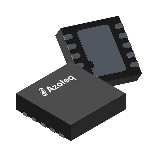
Packaging and Pin-Out
DFN(3x3)-10
Pin 1 marking
1
GPIO0/RDY
2
VDDHI
3
VREG
4
GPIO3/LTX
5
IQS620A 1 i
z WWYY
SDA
10
VSS
9
NC
8
SCL
7
RX1
6
RX0
Landing pad = VSS
Figure 1.2
IQS620A pin-out (DFN(3x3)-10 package top view; markings may differ)
Table 1.1
DFN(3x3)-10 pin-out description
IQS620A in DFN(3x3)-10
Pin
1
2
Name
Type
Function
SDA
GPIO0 /
RDY
VDDHI
VREG
Digital input / output
Digital output
Open drain active low logic
Supply input
Voltage regulator output
5
GPIO3 /
LTX
Digital output /
Analogue transmitter electrode
6
RX0
Analogue receiving electrode
7
RX1
Analogue receiving electrode
8
9
10
SCL
NC
VSS
Digital input / output
Not connect
Supply input
3
4
Copyright © Azoteq (Pty) Ltd 2020
All Rights Reserved
(I2C
SDA
Data signal)
SAR activation output (higher priority)
RDY (I2C Ready interrupt signal; lower priority)
Supply: IQS620A: 1.8V(-2%) – 3.3V
Regulates the system’s internal voltage
Requires external capacitors to ground
PWM signal output (higher priority) /
Connect to inductive sensor’s transmitting coil (lower
priority)
Connect to conductive area intended for sensor
receiving
Connect to conductive area intended for sensor
receiving
SCL (I2C Clock signal)
Not connect
Common ground reference
IQS620A datasheet revision 3.00
Shortcut to memory map
Page 6 of 94
September 2020
�IQ Switch
ProxFusion® Series
1.2.2
WLCSP-9
Pin 1 Marking
Figure 1.3
1
2
3
A
SCL
GPIO3/
LTX
GPIO0/
RDY
B
RX1
RX0
SDA
C
VSS
VREG
VDDHI
IQS620A pin-out (WLCSP-9 package top view; markings may differ)
Table 1.2
WLCSP-9 pin-out description
IQS620A in WLCSP-9
Pin
Name
Type
A1
A2
SCL
GPIO3 /
LTX
Digital input / output
Digital output /
Analogue transmitter electrode
A3
B1
GPIO0 /
RDY
RX1
Digital output
Open drain active low logic
Analogue receiving electrode
B2
RX0
Analogue receiving electrode
B3
C1
C2
SDA
VSS
VREG
Digital input / output
Supply input
Voltage regulator output
C3
VDDHI
Supply input
Copyright © Azoteq (Pty) Ltd 2020
All Rights Reserved
Function
SCL (I2C Clock signal)
PWM signal output (higher priority) /
Connect to inductive sensor’s transmitting coil (lower
priority)
SAR activation output (higher priority)
RDY (I2C Ready interrupt signal; lower priority)
Connect to conductive area intended for sensor
receiving
Connect to conductive area intended for sensor
receiving
SDA (I2C Data signal)
Common ground reference
Regulates the system’s internal voltage
Requires external capacitors to ground
Supply: IQS620A: 1.8V(-2%) – 3.3V
IQS620A datasheet revision 3.00
Shortcut to memory map
Page 7 of 94
September 2020
�IQ Switch
ProxFusion® Series
1.3
Reference schematic
Figure 1.4
Figure 1.5
IQS620A DFN(3x3)-10 reference schematic
IQS620A WLCSP-9 reference schematic
Please note:
−
−
−
−
C1, C2 and C3 should be placed as close as possible to the IQS620A package and should
terminate using the shortest possible path to the IQS GND connection pin.
R4 & R5 are recommend 0603 ESD protection resistors but also aid in sensor RF immunity.
The values can be increased up to 4kΩ for severe RF noise environments.
C4 & C5 are optional loading capacitors and should only be used if intended to de-sensitize
sensors or match one sensor’s capacitive load with another electrode implementation.
VR1 & VR2 are optional TVS diodes for ESD clamping and noise suppression. Ensure the
correct layout principles are followed when placed and routed.
Copyright © Azoteq (Pty) Ltd 2020
All Rights Reserved
IQS620A datasheet revision 3.00
Shortcut to memory map
Page 8 of 94
September 2020
�IQ Switch
ProxFusion® Series
1.3.2
Recommended VREG and VDDHI capacitor ratio
For supplies with low in-line resistance and high current output capability is it recommended to
ensure CVREG > 2CVDDHI. This is to prevent a known ESD risk.
Known risk: The IQS620A will not recover from ESD events if the following conditions are met:
>
>
VDDHI source is present with low impedance path and high current sourcing capability
CVDDHI > CVREG
With these conditions met, the source keeps VDDHI above the BODVDDHI level during the ESD
event but drains the VREG capacitor during sleep mode causing a unique sleep-mode BOD event
keeping the IC in reset. This only recovers when forcing a POR on VDDHI.
For supplies with a high in-line resistance (such as battery with high series resistance) it is
recommended to ensure CVDDHI > CVREG to prevent an unexpected dip on VDDHI when the sensor
wakes from sleep-mode and re-charging the VREG capacitor.
Table 1.3
CVREG minimum and recommended CVDDHI capacitor values
Report rate minimum
(Slowest sampling
rate allowed)
15.625Hz
(64ms)
7.8Hz
(128ms)
6.25Hz
(160ms)
3.9Hz
(256ms)
Recommended
for general
design
2.2µF
2.2µF
3.3µF
3.9µF
4.7µF
CVDDHI recommended †
1µF
1µF
1.5µF
1.5µF
2.2µF
Suitable for Hall-effect
No
No
No
No
Yes
CVREG minimum*
For applications that requires Hall-effect channel conversions a minimum CVREG = 4.7µF is
mandatory to ensure stable regulation during Hall-effect plate sampling.
*
Based on sleep mode current consumption of “Isleep” with starting voltage “VREG” minimum voltage and discharge voltage > BODVREG
maximum at the end of the sleep period
†
Based on CVREG > 2CVDDHI
Copyright © Azoteq (Pty) Ltd 2020
All Rights Reserved
IQS620A datasheet revision 3.00
Shortcut to memory map
Page 9 of 94
September 2020
�IQ Switch
ProxFusion® Series
1.4
Sensor channel combinations
The table below summarizes the IQS620A’s sensor and channel associations.
Capacitive
Table 1.4
Sensor - channel allocation
Sensor /
UI type
CH0
CH1
CH2
Self capacitive
ͦ
ͦ
ͦ
SAR UI 1CH
self (2 level +
movement)
•
Main
•
Movement
SAR UI 2CH
self (3 level)
•
•
Hall-effect
Inductive
CH4
CH5
•
Positive
•
Negative
•
•
Hysteresis UI
Hall-effect
switch UI
Inductive
resonant tank
ͦ
ͦ
ͦ
Inductive
mutually
coupled coils
ͦ
ͦ
ͦ
Hysteresis UI
Temperature
CH3
Temperature
monitoring
•
•
Key:
o - Optional implementation
•
- Fixed use for UI
Copyright © Azoteq (Pty) Ltd 2020
All Rights Reserved
IQS620A datasheet revision 3.00
Shortcut to memory map
Page 10 of 94
September 2020
�IQ Switch
ProxFusion® Series
1.5
ProxFusion® Sensitivity
The measurement circuitry uses a temperature stable internal sample capacitor (CS) and internal
regulated voltage (VREG). Internal regulation provides for more accurate measurements.
The Automatic Tuning Implementation (ATI) is a sophisticated technology implemented on the
ProxFusion® device series. It allows for optimal performance of the devices for a wide range of
sense electrode capacitances, without modification or addition of external components. The ATI
functionality ensures that sensor sensitivity is not affected by external influences such as
temperate, parasitic capacitance and ground reference changes.
The ATI process adjusts three values (Coarse multiplier, Fine multiplier, Compensation) using two
parameters (ATI base and ATI target) as inputs. A 10-bit compensation value ensures that an
accurate target is reached. The base value influences the overall sensitivity of the channel and
establishes a base count for the ATI algorithm. A rough estimation of sensitivity can be
approximated using the relation:
𝑇𝑎𝑟𝑔𝑒𝑡
𝐵𝑎𝑠𝑒
As seen from this equation, the sensitivity can be increased by either increasing the Target value
or decreasing the Base value. A lower base value will typically result in lower multipliers and more
compensation would be required. It should, however, be noted that a higher sensitivity will yield a
higher noise susceptibility. Refer to Appendix B for more information regarding Hall-effect ATI.
𝑆𝑒𝑛𝑠𝑖𝑡𝑖𝑣𝑖𝑡𝑦 ∝
Copyright © Azoteq (Pty) Ltd 2020
All Rights Reserved
IQS620A datasheet revision 3.00
Shortcut to memory map
Page 11 of 94
September 2020
�IQ Switch
ProxFusion® Series
2
Capacitive sensing
Introduction to ProxSense®
2.1
Building on the previous successes from the ProxSense® range of capacitive sensors, the same
fundamental sensor engine has been implemented in the ProxFusion® series.
The capacitive sensing capabilities of the IQS620A include:
•
•
•
•
•
•
Self-capacitive sensing.
Maximum of 3 capacitive channels to be individually configured.
o Individual sensitivity setups
o Alternative ATI modes
Discreet button UI:
o Fully configurable 2 level threshold setups for prox & touch activation levels.
o Customizable filter halt time
Single channel SAR UI:
o For passing the SAR qualification
o Movement sensing to distinguish between stationary in-contact objects and human
interference
o Quick release detection feature (fully configurable)
o GPIO output of SAR activation (on GPIO0) for driving e.g. WWAN module directly
o Up to three triggers levels (proximity, touch and deep touch) for dynamic power
reduction
o All triggers offer never time-out capability
Two Channel SAR UI:
o For passing the SAR qualification latest requirements (EN50566)
o Up to three dedicated triggers levels per sensor for dynamic power reduction
o All triggers offer never time-out capability
Hysteresis UI:
o 4 Optional prox and touch activation hysteresis selections.
o Fully configurable 2 level threshold setups for prox & touch activation levels.
o Customizable filter halt time
Copyright © Azoteq (Pty) Ltd 2020
All Rights Reserved
IQS620A datasheet revision 3.00
Shortcut to memory map
Page 12 of 94
September 2020
�IQ Switch
ProxFusion® Series
2.2
Channel specifications
The IQS620A provides a maximum of 3 channels available to be configured for capacitive sensing.
Each channel can be setup separately according to the channel’s associated settings registers.
There are three distinct capacitive user interfaces available to be used.
a) Self capacitive proximity/touch UI
b) SAR UIs
c) Hysteresis UI
When the single channel SAR UI is activated (ProxFusion Settings4: bit7-6):
•
Channel 0 is used for the main capacitive sensing channel for SAR detection and release
detection.
•
Channel 1 is used for capacitive movement detection.
When the two channel SAR UI is active (ProxFusion Settings4: bit7-6):
•
Channel 0 & 1 is used for the first or main SAR antenna sensor (Rx0)
•
Channel 2 is used for a second SAR antenna sensor (Rx1)
Table 2.1
Capacitive sensing - channel allocation
Mode
CH0
CH1
CH2
Self
capacitive
ͦ
ͦ
ͦ
Single SAR
UI self
•
Main
•
Movement
Two channel
SAR UI self
•
•
Hysteresis UI
CH3
CH4
CH5
•
•
Key:
o - Optional implementation
• - Fixed use for UI
Copyright © Azoteq (Pty) Ltd 2020
All Rights Reserved
IQS620A datasheet revision 3.00
Shortcut to memory map
Page 13 of 94
September 2020
�IQ Switch
ProxFusion® Series
2.3
Hardware configuration
In the table below are multiple options of configuring sensing (Rx) electrodes to realize different
implementations (combinations not shown).
Table 2.2
Capacitive sensing - hardware description
Self capacitive configuration
1 button
2
buttons
Single
SAR
antenna
Two
SAR
antenna
Copyright © Azoteq (Pty) Ltd 2020
All Rights Reserved
RX1
RX0
RX1
RX0
RX1
RX0
RX1
RX0
IQS620A datasheet revision 3.00
Shortcut to memory map
Page 14 of 94
September 2020
�IQ Switch
ProxFusion® Series
2.4
Software configuration
2.4.1
Registers to configure for capacitive sensing:
Table 2.3
Address
Name
Capacitive sensing settings registers
Description
Recommended setting
ProxFusion Settings 0
Sensor mode and
configuration of each channel.
Sensor mode should be set to
capacitive mode
An appropriate RX should be
chosen
0x43
0x44
0x45
ProxFusion Settings 1
Channel settings for the
ProxSense sensors
Full ATI is recommended for fully
automated sensor tuning.
0x46
0x47
0x48
ProxFusion Settings 2
ATI settings for ProxSense
sensors
ATI target should be more than
ATI base to achieve an ATI
0x49
0x4A
0x4B
ProxFusion Settings 3
Additional Global settings for
ProxSense sensors
None
ProxFusion Settings 4
UI enable command and filter
settings
Choose Normal 2 Channel,
Single SAR or 3 level dual SAR
UI
ProxFusion Settings 5
Advance sensor settings
None
0x40
0x41
0x42
0x50
0x51
2.4.2
Registers to configure for the standard UI (proximity / touch):
Please note: If the standard UI (proximity / touch) is used then the single SAR UI (proximity / touch
/ movement) cannot be used and the special SAR registers should not be configured or used.
Initializing inactive UI registers can corrupt other active UI’s.
Table 2.4
Address
Name
standard UI settings registers
Description
0x60
0x62
0x64
Proximity threshold
0x61
0x63
0x65
Touch threshold
Touch Thresholds for all capacitive channels
ProxFusion standard UI
Halt timeout setting for all capacitive channels
0x66
2.4.3
Proximity Thresholds for all capacitive channels (except for single
channel SAR active on channel 0)
halt time
Registers to configure for the two channel SAR UI (proximity / touch / deep touch):
Please note: If the two channel SAR UI is used then the special SAR UI registers (proximity,
movement, release detection) cannot be used and the settings registers should be used as shown
in the table below. Initializing inactive UI registers can corrupt other active UI’s.
Copyright © Azoteq (Pty) Ltd 2020
All Rights Reserved
IQS620A datasheet revision 3.00
Shortcut to memory map
Page 15 of 94
September 2020
�IQ Switch
ProxFusion® Series
Table 2.5
Address
0x50
0x80
0x60
0x61
0x63
0x81
0x82
0x83
0x66
Name
Two channel SAR UI settings registers
Description
ProxFusion settings 4
Two channel SAR UI enable command (bit7-6).
Hysteresis settings
Disable Hysteresis for proximity and touch thresholds
CH0 Proximity threshold
SAR Antenna 1 proximity threshold
CH0 Touch threshold
SAR Antenna 1 touch threshold
CH1 Touch threshold
SAR Antenna 1 deep touch threshold
CH2 filter halt threshold
SAR Antenna 2 proximity threshold
CH2 proximity threshold
SAR Antenna 2 touch threshold
CH2 touch threshold
SAR Antenna 2 deep touch threshold
ProxFusion standard UI
Halt timeout setting for all capacitive channels. Set to 0xFF for no
halt time
time-out as required by SAR applications
Copyright © Azoteq (Pty) Ltd 2020
All Rights Reserved
IQS620A datasheet revision 3.00
Shortcut to memory map
Page 16 of 94
September 2020
�IQ Switch
ProxFusion® Series
2.4.4
Registers to configure for the single channel SAR UI:
Please note: If the single SAR UI is used then the discreet button UI cannot be used and the
ProxFusion discrete UI settings registers should not be configured or used. Initializing inactive UI
registers can corrupt other active UI’s.
Table 2.6
Address
Name
ProxFusion settings 4
0x50
Description
Single channel SAR UI (prox / touch / movement) enable command
(bit7-6).
SAR UI Settings 0
0x70
Filter settings for movement and QRD,
SAR activation output to GPIO0 (RDY signal disabled)
0x71
0x72
0x73
0x74
SAR UI Settings 0
LTA halt timeout and movement threshold settings
Quick release threshold
Threshold setting to trigger a quick release based on the Quick
Ch0
release count values in register 0xF2 & 0xF3.
Filter halt threshold Ch0
Threshold value for channel 0 LTA filter halt
SAR Proximity threshold
Proximity threshold used for SAR activations on channel 0
Ch0
Quick release halt time
0x75
2.4.5
Single channel SAR UI settings registers
Halt timeout setting for channel 0 LTA after a quick release trigger
with zero movement
Registers to configure for the Hysteresis UI:
Please note: Only channel 2 can be used with the Hysteresis UI. Please setup channel 2
accordingly if required. The Hysteresis UI can be used simultaneously with the discrete button UI
or SAR UI.
Table 2.7
Address
Hysteresis UI settings registers
Name
Description
0x50
ProxFusion settings 4
Hysteresis UI enable command (bit6).
0x80
Hysteresis UI settings
Hysteresis selection options for prox and touch activations
Hysteresis UI filter halt
UI filter halt threshold value to halt the LTA value from following
0x81
0x82
0x83
2.4.6
threshold
Hysteresis UI prox
Threshold setting to trigger a prox activation on channel 2 data.
threshold
Hysteresis UI touch
Threshold value to trigger a touch activation on channel 2 data.
threshold
Example code:
Example code for an Arduino Uno can be downloaded at:
www.azoteq.com//images/stories/software/IQS62x_Demo.zip
Copyright © Azoteq (Pty) Ltd 2020
All Rights Reserved
IQS620A datasheet revision 3.00
Shortcut to memory map
Page 17 of 94
September 2020
�IQ Switch
ProxFusion® Series
2.5
Sensor data output and flags
The following registers should be monitored by the master to detect capacitive sensor output and
SAR activations.
a) The Global events register (0x11) will show the IQS620A’s main events. Bit0 is dedicated
to the ProxSense activations and two other bits (bit7 & bit1) is provided to show the state of
the single channel SAR UI. SINGLE_SAR_ACTIVE (bit7) will be constantly active during
SAR detection. SAR event (bit1) will toggle upon each SAR qualified event or change of
SAR status. Bit3 is dedicated to the Hysteresis UI activations (for ch2 data only).
Global Events (0x11)
Bit
Number
7
6
5
4
3
2
1
0
Data
Access
R
R
R
R
R
R
R
R
Name
SINGLE
SAR
ACTIVE
PMU
EVENT
SYS
EVENT
TEMP
EVENT
HYSTERESIS UI
EVENT
HALL
EVENT
SINGLE
SAR
EVENT
PROX
SENSE
EVENT
b) The ProxFusion UI flags (0x12) and SAR UI flags (0x13) provide more detail regarding
the outputs. A prox and touch output bit for each channel 0 to 2 is provided in the
ProxFusion UI flags register.
c) The SAR UI Flags (0x13) register will show detail regarding the state of the SAR output as
well as Quick release toggles, movement activations and the state of the filter (halted or
not). The SAR UI can also be used with the inductive sensing capabilities and is explained
in section 4. Inductive sensing.
ProxFusion UI flags (0x12)
Bit
Number
7
6
5
4
3
2
1
0
Data
Access
-
R
R
R
-
R
R
R
Name
-
CH2_T
CH1_T
CH0_T
-
CH2_P
CH1_P
CH0_P
SAR UI flags (0x13)
Bit
Number
7
6
5
4
3
2
1
0
Data
Access
-
-
-
R
-
R
R
R
Name
-
-
-
SAR
ACTIVE
-
QUICK
RELEASE
MOVEMENT
FHALT
Hysteresis UI flags (0x13)
Bit
Number
7
6
5
4
3
2
1
0
Data
Access
R
R
R
-
-
-
-
-
Name
Signed
output
TOUCH
PROX
-
-
-
-
-
d) When the “Two channel SAR UI” is chosen for proximity, touch and deep touch on two
channels, the ProxFusion UI flags and Hysteresis UI flags are defined as shown below:
Copyright © Azoteq (Pty) Ltd 2020
All Rights Reserved
IQS620A datasheet revision 3.00
Shortcut to memory map
Page 18 of 94
September 2020
�IQ Switch
ProxFusion® Series
Two channel SAR UI flags (0x12)
Bit
Number
7
6
5
4
3
2
1
0
Data
Access
-
R
R
R
-
R
R
R
Name
-
-
ANT 1
DEEP
TOUCH
ANT 1
TOUCH
-
ANT 2
PROX
-
ANT 1
PROX
Two channel SAR UI flags 2 (0x13)
Bit
Number
7
6
5
4
3
2
1
0
Data
Access
R
R
R
R
-
R
R
R
Name
-
ANT 2
DEEP
TOUCH
ANT 2
TOUCH
-
-
-
-
-
Copyright © Azoteq (Pty) Ltd 2020
All Rights Reserved
IQS620A datasheet revision 3.00
Shortcut to memory map
Page 19 of 94
September 2020
�IQ Switch
ProxFusion® Series
3
Hall-effect sensing
3.1
Introduction to Hall-effect sensing
The IQS620A has an internal Hall-effect sensing plate (on chip). No external sensing hardware is
required for Hall-effect sensing.
The Hall-effect sensor measures the generated voltage difference across the plate, which can be
modelled as a Wheatstone bridge. The voltage difference is converted to a current using an
operational amplifier in order to be measured by the same ProxSense® sensor engine.
Advanced digital signal processing is performed to provide sensible output data.
•
•
•
•
3.2
Two threshold levels are provided (prox & touch).
Hall-effect output can be linearized through a selectable inverse calculator option.
North/South field direction indication provided.
Differential Hall-Effect sensing:
o Removes common mode disturbances
o North-South field indication
Channel specifications
Channels 4 and 5 are dedicated to Hall-effect sensing. Channel 4 performs the positive direction
measurements and channel 5 will handle all measurements in the negative direction. These two
channels are used in conjunction to acquire differential Hall-effect data and will always be used as
input data to the Hall-effect UI’s.
There are two distinct Hall-effect user interfaces available:
a) General Hall-effect sensing
b) Hall-effect switch UI
Table 3.1
Mode
CH0
Hall-effect sensor – channel allocation
CH1
CH2
CH3
CH4
CH5
•
Positive
•
Negative
Hall-effect
switch UI
Smart cover
Slide switch
Key:
o - Optional implementation
• - Fixed use for UI
Copyright © Azoteq (Pty) Ltd 2020
All Rights Reserved
IQS620A datasheet revision 3.00
Shortcut to memory map
Page 20 of 94
September 2020
�IQ Switch
ProxFusion® Series
3.3
Hardware configuration
Rudimentary hardware configurations
Axially polarized magnet (linear movement or magnet presence detection)
Hall-effect
push
switch
Smart
cover
Bar magnet (linear movement and magnet field detection)
Slide
switch
Copyright © Azoteq (Pty) Ltd 2020
All Rights Reserved
IQS620A datasheet revision 3.00
Shortcut to memory map
Page 21 of 94
September 2020
�IQ Switch
ProxFusion® Series
3.4
Software configuration
3.4.1
Registers to configure for Hall-effect sensing:
Table 3.2
Address
Name
Hall-effect settings 0
Hall-effect sensing settings registers
Description
Recommended setting
Charge frequency divider and
Charge frequency adjusts the
ATI mode settings
conversion rate of the Hall-effect
channels. Faster conversions
0x90
consume less current.
Full ATI is recommended for fully
automated sensor tuning.
0x91
0xA0
0xA1
0xA2
3.4.2
Hall-effect settings 1
ATI base and target
ATI target should be more than
selections
ATI base to achieve an ATI
Hall-effect switch UI
Various settings for the Hall-
None
settings
effect switch UI
Hall-effect switch UI
Proximity Threshold for UI
Less than touch threshold
Touch Threshold for UI
None
proximity threshold
Hall-effect switch UI
touch threshold
Example code:
Example code for an Arduino Uno can be downloaded at:
www.azoteq.com//images/stories/software/IQS62x_Demo.zip
Copyright © Azoteq (Pty) Ltd 2020
All Rights Reserved
IQS620A datasheet revision 3.00
Shortcut to memory map
Page 22 of 94
September 2020
�IQ Switch
ProxFusion® Series
3.5
Sensor data output and flags
The following registers can be monitored by the master to detect Hall-effect related events.
a) One bit in the Global events (0x11) register is dedicated to the Hall-effect output. Bit2
HALL_EVENT will be toggled for any Hall-effect UI detections.
Global events (0x11)
Bit
Number
7
6
5
4
3
2
1
0
Data
Access
R
R
R
R
R
R
R
R
Name
SAR
ACTIVE
PMU
EVENT
SYS
EVENT
TEMP
EVENT
HYSTERESIS UI
EVENT
HALL
EVENT
SAR
EVENT
PROX
SENSE
EVENT
b) The Hall-effect UI flags (0x16) register provides the standard two-level activation output
(prox = HALL_POUT & touch = HALL_TOUT) as well as a HALL_N/S bit to indicate the
magnet polarity orientation.
Hall-effect UI flags (0x16)
Bit
Number
7
6
5
4
3
2
1
0
Data
Access
-
-
-
-
-
R
R
R
Name
-
-
-
-
-
HALL
TOUT
HALL
POUT
HALL
N/S
c) The Hall-effect UI output (0x17 & 0x18) registers provide a 16-bit value of the Hall-effect
amplitude detected by the sensor.
Hall-effect UI Output (0x17 - 0x18)
Bit
Number
7
6
5
4
3
2
1
0
Data
Access
R
R
R
R
R
R
R
R
Name
Hall-effect UI output low byte
Bit
Number
15
14
13
12
11
10
9
8
Data
Access
R
R
R
R
R
R
R
R
Name
Copyright © Azoteq (Pty) Ltd 2020
All Rights Reserved
Hall-effect UI output high byte
IQS620A datasheet revision 3.00
Shortcut to memory map
Page 23 of 94
September 2020
�IQ Switch
ProxFusion® Series
4
Inductive sensing
4.1
Introduction to inductive sensing
The IQS620A provides inductive sensing capabilities in order to detect the presence of
metal/metal-type objects. Prox and touch thresholds are widely adjustable and individual hysteresis
settings are definable for each using the Hysteresis UI.
4.2
Channel specifications
The IQS620A requires both Rx sensing pins as well as the Tx pin for inductive sensing.
Channels 0, 1 and/or 2 can be setup for inductive sensing although only channel 2 can be used for
the Hysteresis UI which is attractive as an inductive data processing UI.
The Hysteresis UI provides superior options for prox and touch activation with filter halt and
hysteresis settings.
a) Hysteresis UI (Dedicated to CH2)
Table 4.1
Inductive sensor – channel allocation
Mode
CH0
CH1
CH2
Inductive
resonant tank
ͦ
ͦ
ͦ
Inductive
mutually
coupled coils
ͦ
ͦ
ͦ
Hysteresis UI
CH3
CH4
CH5
•
Key:
o
•
- Optional implementation
- Fixed use for UI
Copyright © Azoteq (Pty) Ltd 2020
All Rights Reserved
IQS620A datasheet revision 3.00
Shortcut to memory map
Page 24 of 94
September 2020
�IQ Switch
ProxFusion® Series
4.3
Hardware configuration
Rudimentary hardware configuration. Please refer to application note AZD115 for design details.
Table 4.2
Inductive hardware description
Inductive resonant tank
Connection
diagram
iewer does not support full S G .
FPCBA 2-layer
coil and target
example
Inductive mutually coupled coils
Connection
diagram
iewer does not support full S G .
Coil examples
Copyright © Azoteq (Pty) Ltd 2020
All Rights Reserved
IQS620A datasheet revision 3.00
Shortcut to memory map
Page 25 of 94
September 2020
�IQ Switch
ProxFusion® Series
4.4
Software configuration
4.4.1
Registers to configure for inductive sensing:
Please note: If the discreet button UI is used then the SAR UI cannot be used, and the SAR
registers should not be configured or used. Initializing inactive UI registers can corrupt other active
UI’s.
Table 4.3
Address
Inductive sensing settings registers
Name
ProxFusion Settings 0
Description
Recommended setting
Sensor mode and
Sensor mode should be set to
configuration of channel 2.
inductive mode
0x42
Both RX0 and RX1 should be
active on channel 2
ProxFusion Settings 1
0x45
ProxFusion Settings 2
0x48
ProxFusion Settings 3
0x4B
Full ATI is recommended for fully
inductive sensor
automated sensor tuning.
ATI settings for the inductive
ATI target should be more than
sensor
ATI base to achieve an ATI
Additional settings for the
None
inductive sensor
ProxFusion Settings 4
0x50
4.4.2
Channel 2 settings for the
UI enable command and filter
Enable the Hysteresis UI filter
settings
according to application
Registers to configure for the Hysteresis UI:
Please note: Only channel 2 can be used with the Hysteresis UI. Please setup channel 2
accordingly if required. The Hysteresis UI can be used simultaneously with the discrete button UI
or SAR UI.
Table 4.4
Address
Name
Hysteresis UI settings registers
Description
0x50
ProxFusion settings 4
Hysteresis UI enable command
0x80
Hysteresis UI Settings
Hysteresis settings for the Hysteresis UI prox and touch output
Hysteresis UI filter halt
Threshold setting to trigger a filter halt for sensor data on channel 2
0x81
0x82
0x83
threshold
Hysteresis UI proximity
Proximity threshold used for sensor data on channel 2
threshold
Hysteresis UI touch
Touch threshold used for sensor data on channel 2
threshold
Copyright © Azoteq (Pty) Ltd 2020
All Rights Reserved
IQS620A datasheet revision 3.00
Shortcut to memory map
Page 26 of 94
September 2020
�IQ Switch
ProxFusion® Series
4.5
Sensor data output and flags
The following registers can be monitored by the master to detect inductive sensor related events.
a) Global events (0x11) to prompt for inductive sensor activation. Bit0 PROXSENSE_EVENT
will indicate the detection of a metal object on any of the channels 0, 1 or 2 using the
discreet mutual inductive sensing UI permitted that the specific channel is setup for
inductive sensing.
b) Bit3 denoted as HYSTERESIS_UI_EVENT will indicate the detection of a metal object
using the hysteresis UI on an inductive sensing channel permitted that the hysteresis UI is
activated.
Global events (0x11)
Bit
Number
7
6
5
4
3
2
1
0
Data
Access
R
R
R
R
R
R
R
R
Name
SAR
ACTIVE
PMU
EVENT
SYS
EVENT
TEMP
EVENT
HYSTERESIS UI
EVENT
HALL
EVENT
SAR
EVENT
PROX
SENSE
EVENT
c) The Hysteresis UI flags (0x13) register provides the classic prox/touch two level activation
outputs as well as a bit to distinguish whether the current counts are above or below the
LTA.
Hysteresis UI flags (0x13)
Bit
Number
7
6
5
4
3
2
1
0
Data
Access
R
R
R
-
-
-
-
-
Name
Signed
output
TOUCH
PROX
-
-
-
-
-
d) Hysteresis UI output (0x14 & 0x15) registers will provide a combined 16-bit value to
acquire the magnitude of the inductive sensed object.
Hysteresis UI output (0x14 - 0x15)
Bit
Number
7
6
5
4
3
2
1
0
Data
Access
R
R
R
R
R
R
R
R
Name
Hysteresis UI output low byte
Bit
Number
15
14
13
12
11
10
9
8
Data
Access
R
R
R
R
R
R
R
R
Name
Copyright © Azoteq (Pty) Ltd 2020
All Rights Reserved
Hysteresis UI output high byte
IQS620A datasheet revision 3.00
Shortcut to memory map
Page 27 of 94
September 2020
�IQ Switch
ProxFusion® Series
5
5.1
Temperature monitoring
Introduction to temperature monitoring
The IQS620A provides temperature monitoring capabilities which can be used for temperature
change detection in order to ensure the integrity of other sensing technology. The use of the
temperature sensor is primarily to reseed other sensor channels to account for sudden changes in
environmental conditions.
The IQS620A uses a linearly proportional to absolute temperature sensor for temperature data.
The temperature output data is given by,
𝑎. 219
𝑇=
+𝑐
𝑏. 𝐶𝐻3
Where 𝑎, 𝑏 and 𝑐 are constants that can be determined to provide a required output data as a
function of device temperature. Additionally, the channel setup must be calculated during a testing
process.
The IQS620AT part(s) have been calibrated during production and will use OTP stored values
calculated for that specific part for parameters 𝑎, 𝑏 and 𝑐 as well as a 4-bit value used for the fine
multiplier setup of channel 3 (default always uses the lowest course multiplier).
Table 5.1
Temperature calibration setting registers and ranges
Parameter
Name
Description
𝒂
𝑴𝒖𝒍𝒕𝒊𝒑𝒍𝒊𝒆𝒓
IQS620
Register
IQS620A
Range
Register
Range
Higher nibble
1 – 16
0xC2
1 – 256
Lower nibble
1 – 16
0xC3
1 – 256
0 – 255
0xC4
0 – 255
0xC2
5.2
𝒃
𝑫𝒊𝒗𝒊𝒅𝒆𝒓
𝒄
𝑶𝒇𝒇𝒔𝒆𝒕
0xC3
Channel specifications
The IQS620A requires only external passive components to do temperature monitoring (no
additional circuitry/components required). The temperature UI will be executed using data from
channel 3.
Mode
Table 5.2
Temperature sensor – channel allocation
CH0
CH1
Temperature
monitoring
CH2
CH3
CH4
CH5
•
Key:
o - Optional implementation
•
- Fixed use for UI
Please note that channels 4 and 5, for Hall-effect sensing, needs to be active in order for the
temperature monitoring UI to execute correctly on version 0 and 1 software versions.
For version 2 & 3 devices Hall-effect channels 4 & 5 may be disabled regardless.
5.3
Hardware configuration
No additional hardware required. Temperature monitoring is realized on-chip.
Copyright © Azoteq (Pty) Ltd 2020
All Rights Reserved
IQS620A datasheet revision 3.00
Shortcut to memory map
Page 28 of 94
September 2020
�IQ Switch
ProxFusion® Series
5.4
Software configuration
5.4.1
Registers to configure for temperature monitoring
For IQS620 only:
Table 5.3
Address
0xC0
Temperature monitoring settings registers
Name
Description
Recommended setting
Temperature UI settings
Channel reseed settings
Reseed enable should be set
Multipliers channel 3
Temperature sensor channel
multiplier selection
Dependent on calibration step
0xC2
Temperature calibration
data 0
4-bit Multiplier (𝑎+1) and 4-bit
divider (𝑏+1) calibration values
Requires sample calibration
0xC3
Temperature calibration
data 1
8-bit Offset (𝑐) calibration
value
Requires sample calibration
0xC1
For IQS620AX:
Table 5.4
Address
0xC0
Temperature monitoring settings registers
Name
Description
Recommended setting
Temperature UI settings
Channel reseed settings
Reseed enable should be set
Multipliers channel 3
Temperature sensor channel
multiplier selection
Dependent on calibration step
8-bit
Multiplier
calibration value
Requires sample calibration
0xC2
Temperature UI calibration
multiplier
8-bit Divider (𝑏+1) calibration
value
Requires sample calibration
0xC3
Temperature calibration UI
divider
Temperature UI offset
8-bit Offset
value
Requires sample calibration
0xC1
0xC4
Copyright © Azoteq (Pty) Ltd 2020
All Rights Reserved
(𝑐)
(𝑎+1)
Defined during fabrication
IQS620AT samples
Defined during fabrication
IQS620AT samples
calibration
IQS620A datasheet revision 3.00
Shortcut to memory map
Defined during fabrication
IQS620AT samples
Defined during fabrication
IQS620AT samples
for
for
for
for
Page 29 of 94
September 2020
�IQ Switch
ProxFusion® Series
5.5
Sensor data output and flags
The following registers can be monitored by the master to detect temperature related events.
e) Global events (0x11) to prompt for temperature trip activation. Bit4 denoted as
TEMP_EVENT will indicate the detection of a temperature event.
Global events (0x11)
Bit
Number
7
6
5
4
3
2
1
0
Data
Access
R
R
R
R
R
R
R
R
Name
SAR
ACTIVE
PMU
EVENT
SYS
EVENT
TEMP
EVENT
HYSTERESIS UI
EVENT
HALL
EVENT
SAR
EVENT
PROX
SENSE
EVENT
f)
The Temperature UI flags (0x19) register provides a temperature trip activation output bit
if the condition of a temperature reseed threshold is tripped.
Temperature UI flags (0x19)
Bit
Number
7
6
5
4
3
2
1
0
Data
Access
R
-
-
-
-
-
-
-
Name
Temp
trip
-
-
-
-
-
-
-
g) Temperature UI output (0x1A & 0x1B) registers will provide a combined (big-endian) 16bit output value for the measured internal IC temperature.
Please note:
• For the IQS620AT part(s) (Device version 1 & 2: HW number 0x02 = 0x82):
o The calibration was done so that the UI output is offset by a decimal value of +100
in order to be able to calculate and represent absolute temperatures below 0C in
the controller arithmetic and temperature UI capabilities.
o Example: Temperature UI output = 20’D → 20C or 90’D → -10C
• For the IQS620AT part(s) (Device version 3: HW number 0x02 = 0x92):
o The calibration was done so that the UI output is offset by a decimal value of +40
in order to be able to calculate and represent absolute temperatures below 0C in
the controller arithmetic and temperature UI capabilities.
o Example: Temperature UI output = 60’D → 20C or 30’D → -10C
Temperature UI output (0x1A – 0x1B)
Bit
Number
Data
Access
Name
Bit
Number
Data
Access
Name
7
6
5
4
3
2
1
0
R
R
R
R
R
R
R
R
Temperature output low byte
15
14
13
12
11
10
9
8
R
R
R
R
R
R
R
R
Copyright © Azoteq (Pty) Ltd 2020
All Rights Reserved
Temperature output high byte
IQS620A datasheet revision 3.00
Shortcut to memory map
Page 30 of 94
September 2020
�IQ Switch
ProxFusion® Series
6
Device clock, power management and mode operation
6.1
Device main oscillator
The IQS620A has a 16MHz main oscillator (default enabled) to clock all system functionality.
An option exists to reduce the main oscillator to 4MHz. This will result in charge transfer
frequencies to be one-quarter of the default implementations. System timers are adjusted so that
timeouts and report rates remain the same if possible.
To set this option this:
o
o
6.2
As a software setting – Set the System_Settings: bit4 = 1, via an I2C command.
As a permanent setting – Set the OTP option in OTP Bank 0: bit2 = 1, using IQS620A PC
software.
Device modes
The IQS620A supports the following modes of operation;
•
•
•
•
Normal mode (Fixed report rate)
Low power mode (Reduced report rate)
Ultra-low power mode (Only channel 0 is sensed for a prox)
Halt mode (Suspended/disabled)
Note: Auto modes must be disabled to enter or exit halt mode.
The device will automatically switch between the different operating modes by default. However,
this Auto mode feature may be disabled by setting the DSBL_AUTO_MODE bit
(Power_mode_settings 0xD2: bit5) to confine device operation to a specific power mode. The
POWER_MODE bits (Power_mode_settings 0xD2: bit4-3) can then be used to specify the desired
mode of operation.
6.2.1
Normal mode
Normal mode is the fully active sensing mode to function at a fixed report rate specified in the
Normal mode report rate (0xD3) register. This 8-bit value is adjustable from 0ms – 255ms in
intervals of 1ms.
Note: The device’s low power oscillator has an accuracy of 4ms.
6.2.2
Low power mode
Low power mode is a reduced sensing mode where all channels are sensed but at a reduced
oscillator speed. The sample rate can be specified in the Low Power mode report rate (0xD4)
register. The 8-bit value is adjustable from 0ms – 255ms in intervals of 1ms. Reduced report rates
also reduce the current consumed by the sensor.
Note: The device’s low power oscillator has an accuracy of 4ms.
6.2.3
Ultra-low power mode
Ultra-low power mode is a reduced sensing mode where only channel 0 is sensed at the ultra low
power report rate. Channels 1 to 5 are only updated (sensed and processed according to each
channels setup) during a normal power update cycle. This NP update cycle rate can be set as a
fraction of the configured ULP mode report rate. There are 8 NP segment fraction options available
(Power_mode_settings: bit2-0) ranging from the fastest, ½ ULP rate to the slowest rate of 1/256 of
the ULP rate. This ensures that channels 1 to 5’s LTA values track any slow changes in sensor
counts (typically seen over a long period for varying environmental conditions).
To enable use of the ultra-low power mode set the EN_ULP_MODE bit (Power_mode_settings:
bit6). The sample rate can be specified in the Ultra-Low Power mode report rate (0xD5) register.
The 8-bit value is adjustable from 0ms – 4sec in increments of 16ms for each decimal integer.
IQS620A wake up (return to normal mode) will occur on prox detection of channel 0.
Copyright © Azoteq (Pty) Ltd 2020
All Rights Reserved
IQS620A datasheet revision 3.00
Shortcut to memory map
Page 31 of 94
September 2020
�IQ Switch
ProxFusion® Series
6.2.4
Halt mode
Halt mode will suspend all sensing and will place the device in a dormant or sleep state. The
device requires an I2C command from a master to explicitly change the power mode out of the halt
state before any sensor functionality can continue.
6.2.5
Mode time
The mode time defines the time period in normal or low power modes before automatically moving
to a slower mode (or finally ULP mode if applicable) if no activations are registered in this time.
This time is set in the Auto Mode Timer (0xD6) register. The 8-bit value is adjustable from 0ms – 2
min in intervals of 500ms.
6.3
System reset
The IQS620A device monitor’s system resets and events.
a) Every device power-on and reset event will set the Show Reset bit (System flags 0x10:
bit7) and the master should explicitly clear this bit by setting the ACK_RESET (bit6) in
System Settings.
b) The system events will also be indicated with the Global events register’s SYS_EVENT bit
(Global events 0x11: bit5) if any system event occur such as a reset. This event will
continuously trigger until the reset has been acknowledged.
Copyright © Azoteq (Pty) Ltd 2020
All Rights Reserved
IQS620A datasheet revision 3.00
Shortcut to memory map
Page 32 of 94
September 2020
�IQ Switch
ProxFusion® Series
7
Communication
I2C module specification
7.1
The device supports a standard two wire I2C interface with the addition of an RDY (ready interrupt)
line. The communications interface of the IQS620A supports the following:
•
•
•
•
Standard-mode I2C protocol compliant for speed up to 100kbits/s.
Faster speeds possible up to 400kbits/s but without Fast-mode minimum fall time fulfilment.
Streaming data as well as event mode.
The master may address the device at any time. If the IQS620A is not in a communication
window, the device will return an ACK after which clock stretching may be induced until a
communication window is entered. Additional communication checks are included in the
main loop in order to reduce the average clock stretching time.
The provided interrupt line (RDY) is an open-drain active low implementation and indicates
a communication window.
•
I2C Read
7.2
To read from the device a current address read can be performed. This assumes that the addresscommand is already setup as desired.
Current Address Read
Start
Control byte
S
Addr + READ
Data n
Data n+1
ACK
Stop
ACK
Figure 7.1
NACK
S
Current Address Read
If the address-command must first be specified, then a random read must be performed. In this
case, a WRITE is initially performed to setup the address-command, and then a repeated start is
used to initiate the READ section.
Random Read
Start
Control byte
S
Addr + WRITE
Addresscommand
ACK
ACK
Figure 7.2
7.3
Start
Control byte
S
Addr + READ
Data n
ACK
Stop
NACK
S
Random Read
I2C Write
To write settings to the device a Data Write is performed. Here the Address-Command is always
required, followed by the relevant data bytes to write to the device.
Data Write
Start
Control byte
S
Addr + WRITE
AddressCommand
Data n
ACK
ACK
Figure 7.3
Copyright © Azoteq (Pty) Ltd 2020
All Rights Reserved
Data n+1
ACK
Stop
ACK
S
I2C Data Write
IQS620A datasheet revision 3.00
Shortcut to memory map
Page 33 of 94
September 2020
�IQ Switch
ProxFusion® Series
7.4
Stop-bit disable option
The IQS620A parts offer:
•
an additional I2C settings register (0xDA) specifically added for stop-bit disable functionality,
•
as well as a RDY timeout period register (0xD9) in order to set the required timeout period
for termination of any communication windows (RDY = Low) if no I2C activity is present on
SDA and SCL pins.
Customers using an MCU with a binary serial-encoder peripheral which is not fully I2C compatible
(but provide some crude serial communication functions) can use this option to configure the
IQS620A so that any auto generated stop command from the serial peripheral can be ignored by
the IQS620A I2C hardware. This will restrict the IQS620A from immediately exiting a
communication window until all required communication has been completed and a stop command
can correctly be transmitted. Please refer to the figures below for serial data transmission
examples.
Please note:
1. Stop-bit disable and enable must be performed at the beginning and end of a
communication window. The first and last I2C register to be written to ensure no unwanted
communication window termination.
2. Leaving the Stop-bit disabled will result in successful reading of registers but will not
execute any commands written over I2C in a communication window being terminated after
an RDY timeout and with no IQS recognised stop command.
3. The default RDY timeout period for IQS620A is purposefully long (10.24ms) for slow
responding MCU hardware architectures. Please set this register according to your
requirements/preference.
4. These options are only available on IQS620A parts and not for IQS620.
Stop-bit Disable
Communication
window open
Start
Control byte
RDY = ↓LOW
S
Addr + WRITE
AddressCommand
ACK
0xDA
Figure 7.4
Disable
stop-bit
ACK
0x81
ACK
Ignored
stop
Continue with
reads / writes
S
…
I2C Stop-bit Disable
Stop-bit Enable
Reads / Writes
Finished
Start
Control byte
…
S
Addr + WRITE
AddressCommand
ACK
Figure 7.5
Copyright © Azoteq (Pty) Ltd 2020
All Rights Reserved
0xDA
Enable
stop-bit
ACK
0x01
ACK
Stop
Communication
window closed
S
RDY = ↑HIGH
I2C Stop-bit Enable
IQS620A datasheet revision 3.00
Shortcut to memory map
Page 34 of 94
September 2020
�IQ Switch
ProxFusion® Series
7.5
Device address and sub-addresses
The default device address is 0x44 = DEFAULT_ADDR.
Alternative sub-address options are definable in the following one-time programmable bits:
OTP Bank0 (bit3; 0; bit1; bit0) = SUB_ADDR_0 to SUB_ADDR_7
a)
b)
c)
d)
e)
f)
g)
h)
7.6
Default address:
Sub-address:
Sub-address:
Sub-address:
Sub-address:
Sub-address:
Sub-address:
Sub-address:
0x44 = DEFAULT_ADDR (0x44)
0x45 = DEFAULT_ADDR (0x44)
0x46 = DEFAULT_ADDR (0x44)
0x47 = DEFAULT_ADDR (0x44)
0x4C = DEFAULT_ADDR (0x44)
0x4D = DEFAULT_ADDR (0x44)
0x4E = DEFAULT_ADDR (0x44)
0x4F = DEFAULT_ADDR (0x44)
OR
OR
OR
OR
OR
OR
OR
OR
SUB_ADDR_0 (0000b)
SUB_ADDR_1 (0001b)
SUB_ADDR_2 (0010b)
SUB_ADDR_3 (0011b)
SUB_ADDR_4 (1000b)
SUB_ADDR_5 (1001b)
SUB_ADDR_6 (1010b)
SUB_ADDR_7 (1011b)
Additional OTP options
7.6.1
Device version 0 (Software number 0x04 = D’04)
All one-time-programmable device options are located in OTP bank0.
OTP bank0
Bit
Number
7
6
5
4
3
2
Name
Internal
use
COMMS
ATI
Internal
use
Internal
use
SUB
ADDRESS
(bit3)
4MHz
1
0
SUB ADDRESS (bit1-0)
Bit definitions:
•
•
•
•
•
Bit 7: Internal use
o Do not set. Leave bit cleared.
Bit 6: Communication mode during ATI
o 0: No streaming events are generated during ATI
o 1: Communication continue as setup regardless of ATI state.
Bit 5,4: Internal use
o Do not configure
Bit 2: Main Clock frequency selection
o 0: Run FOSC at 16MHz
o 1: Run FOSC at 4MHz
Bit 3,1,0: I2C sub-address
o I2C address = 0x44 OR SUB_ADDR
Copyright © Azoteq (Pty) Ltd 2020
All Rights Reserved
IQS620A datasheet revision 3.00
Shortcut to memory map
Page 35 of 94
September 2020
�IQ Switch
ProxFusion® Series
7.6.2
Device version 1 (Software number 0x08 = D’08)
All one-time-programmable device options are located in OTP bank0.
OTP bank0
Bit
Number
7
6
5
4
3
2
Name
Internal
use
COMMS
ATI
Internal
use
Internal
use
SUB
ADDRESS
(bit3)
4MHz
1
0
SUB ADDRESS (bit1-0)
Bit definitions:
•
•
•
•
•
7.6.3
Bit 7: Internal use
o Do not set. Leave bit cleared.
Bit 6: Communication mode during ATI
o 0: No streaming events are generated during ATI
o 1: Communication continue as setup regardless of ATI state.
Bit 5,4: Internal use
o Do not configure
Bit 2: Main Clock frequency selection
o 0: Run FOSC at 16MHz
o 1: Run FOSC at 4MHz
Bit 3,1,0: I2C sub-address
o I2C address = 0x44 OR SUB_ADDR
Device version 2 & 3 (Software number 0x0D = D’13)
All one-time-programmable device options are located in OTP bank0.
OTP bank0
Bit
Number
7
6
5
4
3
2
Name
Disable
Hall
COMMS
ATI
Internal
use
Internal
use
SUB
ADDRESS
(bit3)
4MHz
1
0
SUB ADDRESS (bit1-0)
Bit definitions:
•
•
•
•
•
Bit 7: Disable Hall
o 0: All sensors are active.
o 1: Hall-effect sensors are disabled permanently. Use this option for 1.8V rated
supplies requiring up to 5% tolerance (absolute minimum VDDHI >= 1.71V).
Bit 6: Communication mode during ATI
o 0: No streaming events are generated during ATI
o 1: Communication continue as setup regardless of ATI state.
Bit 5,4: Internal use
o Do not configure
Bit 2: Main Clock frequency selection
o 0: Run FOSC at 16MHz
o 1: Run FOSC at 4MHz
Bit 3,1,0: I2C sub-address
o I2C address = 0x44 OR SUB_ADDR
Copyright © Azoteq (Pty) Ltd 2020
All Rights Reserved
IQS620A datasheet revision 3.00
Shortcut to memory map
Page 36 of 94
September 2020
�IQ Switch
ProxFusion® Series
7.7
Recommended communication and runtime flow diagram
The following is a basic master program flow diagram to communicate and handle the device. It
addresses possible device events such as output events, ATI and system events (resets).
POR
Clear
Show_Reset
Reset
occured
Show Reset?
Setup &
Initialization
ATI
No
Yes
IN ATI?
Yes
Runtime
Global Event?
No
System Event?
Yes
Valid event?
No
Yes
Retrieve
event data
Figure 7.6
Master command structure and runtime event handling flow diagram
It is recommended that the master verifies the status of the System_Flags0 bits to identify events
and resets. Detecting either one of these should prompt the master to the next steps of handling
the IQS620A.
Streaming mode communication is used for detail sensor evaluation during prototyping and/or
development phases.
Event mode communication is recommended for runtime use of the IQS620A. This reduces the
communication on the I2C bus and report only triggered events.
Copyright © Azoteq (Pty) Ltd 2020
All Rights Reserved
IQS620A datasheet revision 3.00
Shortcut to memory map
Page 37 of 94
September 2020
�IQ Switch
ProxFusion® Series
8
Memory map
Table 8.1
Full
Address
IQS620A Memory map index
Item Name
Data
Access
Product number
Read-Only
Software number
Read-Only
0x02
Hardware number
Read-Only
0x10
System flags
Read-Only
0x11
Global events
Read-Only
0x12
ProxFusion UI flags
Read-Only
0x13
SAR and Hysteresis UI flags
Read-Only
0x14
Hysteresis UI output 0
Read-Only
Hysteresis UI output 1
Read-Only
Hall-effect UI flags
Read-Only
0x17
Hall-effect UI output 0
Read-Only
0x18
Hall-effect UI output 1
Read-Only
0x19
Temperature UI flags
Read-Only
0x1A
Temperature UI output 0
Read-Only
0x1B
Temperature UI output 1
Read-Only
0x20
Channel 0 counts low
Read-Only
0x21
Channel 0 counts high
Read-Only
0x22
Channel 1 counts low
Read-Only
0x23
Channel 1 counts high
Read-Only
0x24
Channel 2 counts low
Read-Only
Channel 2 counts high
Read-Only
Channel 3 counts low
Read-Only
0x27
Channel 3 counts high
Read-Only
0x28
Channel 4 counts low
Read-Only
0x29
Channel 4 counts high
Read-Only
0x2A
Channel 5 counts low
Read-Only
0x2B
Channel 5 counts high
Read-Only
0x30
Channel 0 LTA low
Read-Write
0x31
Channel 0 LTA high
Read-Write
Channel 1 LTA low
Read-Write
Channel 1 LTA high
Read-Write
0x34
Channel 2 LTA low
Read-Write
0x35
Channel 2 LTA high
Read-Write
Group Name
0x00
0x01
0x15
0x16
0x25
0x26
0x32
0x33
Device information data
Flags and user interface data
Channel counts (raw data)
LTA values (filtered data)
Copyright © Azoteq (Pty) Ltd 2020
All Rights Reserved
IQS620A datasheet revision 3.00
Shortcut to memory map
Page 38 of 94
September 2020
�IQ Switch
ProxFusion® Series
0x40
ProxFusion settings 0_0
Read-Write
0x41
ProxFusion settings 0_1
Read-Write
0x42
ProxFusion settings 0_2
Read-Write
0x43
ProxFusion settings 1_0
Read-Write
0x44
ProxFusion settings 1_1
Read-Write
ProxFusion settings 1_2
Read-Write
ProxFusion settings 2_0
Read-Write
0x47
ProxFusion settings 2_1
Read-Write
0x48
ProxFusion settings 2_2
Read-Write
0x49
ProxFusion settings 3_0
Read-Write
0x4A
ProxFusion settings 3_1
Read-Write
0x4B
ProxFusion settings 3_2
Read-Write
0x50
ProxFusion settings 4
Read-Write
0x51
ProxFusion settings 5
Read-Write
0x52
Compensation Ch0
Read-Write
Compensation Ch1
Read-Write
Compensation Ch2
Read-Write
0x55
Multipliers Ch0
Read-Write
0x56
Multipliers Ch1
Read-Write
0x57
Multipliers Ch2
Read-Write
0x60
Prox threshold Ch0
Read-Write
0x61
Touch threshold Ch0
Read-Write
0x62
Prox threshold Ch1
Read-Write
Touch threshold Ch1
Read-Write
0x64
Prox threshold Ch2
Read-Write
0x65
Touch threshold Ch2
Read-Write
0x66
ProxFusion discrete UI halt time
Read-Write
0x70
SAR UI settings 0
Read-Write
0x71
SAR UI settings 1
Read-Write
QRD threshold Ch0
Read-Write
Filter halt threshold Ch0
Read-Write
0x74
Prox threshold Ch0
Read-Write
0x75
Quick release detection halt time
Read-Write
0x80
Hysteresis UI settings
Read-Write
Hysteresis UI filter halt threshold
Read-Write
Hysteresis UI prox threshold
Read-Write
Hysteresis UI touch threshold
Read-Write
0x45
0x46
0x53
0x54
0x63
0x72
0x73
0x81
0x82
ProxFusion sensor settings
block 0
ProxFusion sensor settings
block 1
ProxFusion UI settings
SAR UI settings
Hysteresis UI settings
0x83
Copyright © Azoteq (Pty) Ltd 2020
All Rights Reserved
IQS620A datasheet revision 3.00
Shortcut to memory map
Page 39 of 94
September 2020
�IQ Switch
ProxFusion® Series
0x90
Hall-effect settings 0
Read-Write
Hall-effect settings 1
Read-Write
Compensation Ch4 and Ch5
Read-Write
0x93
Multipliers Ch4 and Ch5
Read-Write
0xA0
Hall-effect switch UI settings
Read-Write
Hall-effect switch UI prox threshold
Read-Write
0xA2
Hall-effect switch UI touch threshold
Read-Write
0xC0
Temperature UI settings
Read-Write
0xC1
Multipliers Ch3
Read-Write
0x91
0x92
0xA1
0xC2
Hall-effect sensor settings
Hall-effect switch UI settings
Temperature UI settings
0xC3
Temp calibration
data0
Temp calibration
data1
Temp calibration
multiplier*
Temp calibration
divider*
Read-Write
Read-Write
0xC4
Temperature calibration offset*
Read-Write
0xD0
System settings
Read-Write
0xD1
Active channels
Read-Write
0xD2
Power mode settings
Read-Write
0xD3
Normal mode report rate
Read-Write
0xD4
Low power mode report rate
Read-Write
Ultra-low power mode report rate
Read-Write
Auto mode time
Read-Write
0xD7
Global event mask
Read-Write
0xD8
PWM duty cycle
Read-Write
0xD9
RDY Timeout period*
Read-Write
0xDA
I2C settings*
Read-Write
0xDB
Channel reseed enable*
Read-Write
0xD5
0xD6
Device and power mode
settings
* Only available for IQS620A v1 & v2
The full memory map is summarized above. Registers are explained individually in the latter part of
this section.
Copyright © Azoteq (Pty) Ltd 2020
All Rights Reserved
IQS620A datasheet revision 3.00
Shortcut to memory map
Page 40 of 94
September 2020
�IQ Switch
ProxFusion® Series
8.2
8.2.1
Device Information Data
Product number
Product number (0x00)
Bit
Number
7
6
5
4
3
2
1
0
Data
Access
R
R
R
R
R
R
R
R
Name
Device Product Number
Bit definitions:
• Bit 7-0: Device Product Number
o 0x4 = D’65: IQS620(A) product number (all versions)
8.2.2
Software number
Software number (0x01)
Bit
Number
7
6
5
4
3
2
1
0
Data
Access
R
R
R
R
R
R
R
R
Name
Device Software Number
Bit definitions:
• Bit 7-0: Device Software Number
o 0x04 = D’04: IQS620 version 0 firmware (pre-production)
o 0x08 = D’08: IQS620A version 1 firmware (production)
o 0x0D = D’13: IQS620A version 2 firmware (update)
8.2.3
Hardware number
Hardware number (0x02)
Bit
Number
7
6
5
4
3
2
1
0
Data
Access
R
R
R
R
R
R
R
R
Name
Device Hardware Number
Bit definitions:
• Bit 7-0: Device Hardware Number
o 0x82 = D’ 30: IQS620 version 0 hardware number
o 0x82 = D’ 30: IQS620A version 1 & 2 hardware number
o 0x92 = D’ 46: IQS620A version 3 hardware number
Copyright © Azoteq (Pty) Ltd 2020
All Rights Reserved
IQS620A datasheet revision 3.00
Shortcut to memory map
Page 41 of 94
September 2020
�IQ Switch
ProxFusion® Series
8.3
8.3.1
Flags and user interface data
System flags
System flags (0x10)
Bit
Number
7
6
5
4
3
2
1
0
Data
Access
R
-
-
R
R
R
R
R
Name
SHOW
RESET
-
-
IN ATI
EVENT
NP SEG
ACTIVE
POWER MODE
Bit definitions:
• Bit 7: Reset Indicator
o 0: No reset event
o 1: A device reset has occurred and needs to be acknowledged.
• Bit 4-3: Active power-mode indicator
o 00: Normal Mode
o 10: Ultra-Low Power Mode
o 01: Low Power Mode
o 11: Halt Mode
• Bit 2: ATI busy indicator
o 0: No CH’s are in ATI
o 1: One or more CH’s are in ATI
• Bit 1: Global Event Indicator
o 0: No new event to service
o 1: An event has occurred and should be serviced
• Bit 0: Normal power segment indicator
o 0: Not performing a normal power update
o 1: Busy performing a normal power update
8.3.2
Global events
Global events (0x11)
Bit
Number
7
6
5
4
3
2
1
0
Data
Access
R
R
R
R
R
R
R
R
Name
SAR
ACTIVE
PMU
EVENT
SYS
EVENT
TEMP
EVENT
HYSTERESIS UI
EVENT
HALL
EVENT
SAR
EVENT
PROX
SENSE
EVENT
Bit definitions:
• Bit 7: SAR activation state
o 0: SAR output inactive
o 1: SAR output active
• Bit 6: Power management unit event flag
o 0: No event to report
o 1: A PMU event occurred
• Bit 5: System event flag
o 0: No event to report
o 1: A system event has occurred
• Bit 4: Temperature event flag
o 0: No event to report
o 1: A temperature event has occurred and should be handled
• Bit 4: Hysteresis UI event flag
o 0: No event to report
o 1: A hysteresis UI event has occurred and should be handled
Copyright © Azoteq (Pty) Ltd 2020
All Rights Reserved
IQS620A datasheet revision 3.00
Shortcut to memory map
Page 42 of 94
September 2020
�IQ Switch
ProxFusion® Series
•
•
•
8.3.3
Bit 2: Hall-effect event flag
o 0: No event to report
o 1: A Hall-effect event has occurred and should be handled
Bit 1: Single channel SAR event flag
o 0: No event to report
o 1: A single channel SAR event has occurred and should be handled
Bit 0: ProxSense event flag
o 0: No event to report
o 1: A capacitive event has occurred and should be handled
ProxFusion UI flags
ProxFusion UI flags (0x12)
Bit
Number
7
6
5
4
3
2
1
0
Data
Access
-
R
R
R
-
R
R
R
Name
-
CH2_T
CH1_T
CH0_T
-
CH2_P
CH1_P
CH0_P
Bit definitions:
• Bit 6: Ch2 touch indicator
o 0: Delta below touch threshold
• Bit 5: Ch1 touch indicator
o 0: Delta below touch threshold
• Bit 4: Ch0 touch indicator
o 0: Delta below touch threshold
• Bit 2: Ch2 proximity indicator
o 0: Delta below prox threshold
• Bit 1: Ch1 proximity indicator
o 0: Delta below prox threshold
• Bit 0: Ch0 proximity indicator
o 0: Delta below prox threshold
8.3.4
o
1: Delta above touch threshold
o
1: Delta above touch threshold
o
1: Delta above touch threshold
o
1: Delta above prox threshold
o
1: Delta above prox threshold
o
1: Delta above prox threshold
Single channel SAR UI flags
Single channel SAR UI flags (0x13)
Bit
Number
7
6
5
4
3
2
1
0
Data
Access
-
-
-
R
-
R
R
R
Name
-
-
-
SAR
ACTIVE
-
QRD
MOVEMENT
FHALT
Bit definitions:
• Bit 4: SAR Standoff Active
o 0: Delta below SAR prox THR
• Bit 2: Quick Release Detection (QRD) indicator
o 0: Quick release not detected
• Bit 1: Movement indicator
o 0: Movement not detected
• Bit 0: Filter Halt indicator
Copyright © Azoteq (Pty) Ltd 2020
All Rights Reserved
o
1: Delta above SAR prox THR
o
1: Quick release detected
o
1: Movement detected
IQS620A datasheet revision 3.00
Shortcut to memory map
Page 43 of 94
September 2020
�IQ Switch
ProxFusion® Series
o
8.3.5
0: Delta below filter halt THR
o
1: Delta above filter halt THR
Hysteresis UI flags
Hysteresis UI flags (0x13)
Bit
Number
7
6
5
4
3
2
1
0
Data
Access
R
R
R
-
-
-
-
-
Name
Signed
output
TOUCH
PROX
-
-
-
-
-
Bit definitions:
• Bit 7: Delta directional signed output
o 0: Counts < LTA. Delta positive
• Bit 6: Hysteresis UI touch indicator
o 0: Delta below touch threshold
• Bit 5: Hysteresis proximity indicator
o 0: Delta below prox threshold
8.3.6
o
1: Counts > LTA. Delta negative
o
1: Delta above touch threshold
o
1: Delta above prox threshold
Hysteresis UI output
Hysteresis UI output (0x14 - 0x15)
Bit
Number
7
6
5
4
3
2
1
0
Data
Access
R
R
R
R
R
R
R
R
Name
Hysteresis UI Output Low Byte
Bit
Number
15
14
13
12
11
10
9
8
Data
Access
R
R
R
R
R
R
R
R
Name
Hysteresis UI Output High Byte
Bit definitions:
• Bit 15-0: Hysteresis UI output value
Copyright © Azoteq (Pty) Ltd 2020
All Rights Reserved
IQS620A datasheet revision 3.00
Shortcut to memory map
Page 44 of 94
September 2020
�IQ Switch
ProxFusion® Series
8.3.7
Hall-effect UI flags
Hall-effect UI flags (0x16)
Bit
Number
7
6
5
4
3
2
1
0
Data
Access
-
-
-
-
-
R
R
R
Name
-
-
-
-
-
TOUCH
PROX
HALL
N/S
Bit definitions:
• Bit 2: Hall-effect touch indicator
o 0: Count delta below touch threshold
• Bit 1: Hall-effect proximity indicator
o 0: Count delta below prox threshold
• Bit 0: Hall-effect North South Field indication
o 0: North field direction present
o
1: Count delta above touch threshold
o
1: Count delta above prox threshold
o
1: South field direction present
Please note: Only for IQS620AXzCSR (CS = WLCSP-9) a flip chip process is used thus:
o 0: South field direction present
o 1: North field direction present
8.3.8
Hall-effect UI output
Hall-effect UI output (0x17/0x18)
Bit
Number
7
6
5
4
3
2
1
0
Data
Access
R
R
R
R
R
R
R
R
Name
Hall-effect UI Output Low Byte
Bit
Number
15
14
13
12
11
10
9
8
Data
Access
R
R
R
R
R
R
R
R
Name
Hall-effect UI Output High Byte
Bit definitions:
• Bit 15-0: Hall-effect UI output
o 0 – 8 000: Hall-effect UI output value
Copyright © Azoteq (Pty) Ltd 2020
All Rights Reserved
IQS620A datasheet revision 3.00
Shortcut to memory map
Page 45 of 94
September 2020
�IQ Switch
ProxFusion® Series
8.3.9
Temperature UI flags
Temperature UI flags (0x19)
Bit
Number
7
6
5
4
3
2
1
0
Data
Access
R
-
-
-
-
-
-
-
Name
Temp trip
-
-
-
-
-
-
-
Bit definitions:
• Bit 7: Temperature trip indicator
o 0: No event to report
o 1: Temperature event occurred
8.3.10 Temperature UI output
Temperature UI output (0x1A – 0x1B)
Bit
Number
7
6
5
4
3
2
1
0
Data
Access
R
R
R
R
R
R
R
R
Name
Temperature output low byte
Bit
Number
15
14
13
12
11
10
9
8
Data
Access
R
R
R
R
R
R
R
R
Name
Temperature output high byte
Bit definitions:
• Bit 15-0: Temperature UI output
o IQS620A: Temperature output value (relative/unitless; uncalibrated)
o IQS620AT (Device version 1 & 2: HW number 0x02 = 0x82):
▪ Temperature output value -100 = Device die temperature (°C)
o IQS620AT (Device version 3: HW number 0x02 = 0x92):
▪ Temperature output value -40 = Device die temperature (°C)
Copyright © Azoteq (Pty) Ltd 2020
All Rights Reserved
IQS620A datasheet revision 3.00
Shortcut to memory map
Page 46 of 94
September 2020
�IQ Switch
ProxFusion® Series
8.4
Channel counts (raw data)
Channel counts Ch0/1/2/3 (0x20/0x21 - 0x2A/0x2B)
Bit
Number
7
6
5
4
3
2
1
0
Data
Access
R
R
R
R
R
R
R
R
Name
Channel Data Low Byte
Bit
Number
15
14
13
12
11
10
9
8
Data
Access
R
R
R
R
R
R
R
R
Name
Channel Data High Byte
Bit definitions:
• Bit 15-0: Channel counts
o AC filtered or raw value counts of ProxFusion sensor channels
8.5
LTA values (filtered data)
LTA Ch0/1/2 (0x30/0x31 - 0x34/0x35)
Bit
Number
7
6
5
4
3
2
1
0
Data
Access
R/W
R/W
R/W
R/W
R/W
R/W
R/W
R/W
Name
LTA Low Byte
Bit
Number
15
14
13
12
11
10
9
8
Data
Access
R/W
R/W
R/W
R/W
R/W
R/W
R/W
R/W
Name
LTA High Byte
Bit definitions:
• Bit 15-0: LTA filter value output
o Long term average value of channels
Copyright © Azoteq (Pty) Ltd 2020
All Rights Reserved
IQS620A datasheet revision 3.00
Shortcut to memory map
Page 47 of 94
September 2020
�IQ Switch
ProxFusion® Series
8.6
8.6.1
ProxFusion sensor settings block 0
ProxFusion settings 0
Capacitive sensing
ProxFusion settings 0_0/1/2 (0x40-0x42)
Bit
Number
7
6
5
4
3
2
1
0
Data
Access
R/W
R/W
-
-
-
-
R/W
R/W
Internal
use
Internal
use
-
RX Select
-
-
-
-
Name
Fixed
value
Capacitive sensor
mode
0
0
Bit definitions:
• Bit 7-6: Sensor Mode
o 00: Capacitive sensing mode
• Bit 1-0: RX Select
o 00: RX0 and RX1 is disabled
o 01: RX0 is enabled
o
o
10: RX1 is enabled
11: RX0 and RX1 is enabled
Inductive sensing
ProxFusion settings 0_0/1/2 (0x40-0x42)
Bit
Number
7
6
5
4
3
2
1
0
Data
Access
R/W
R/W
-
R/W
-
-
R/W
R/W
Internal
use
Multiplier
range
-
-
-
-
Name
Fixed
value
Inductive sensor
mode
1
0
RX Select
1
1
Bit definitions:
• Bit 7-6: Sensor Mode
o 10: Inductive sensor mode
• Bit 4: Multiplier range
o 0: Large
o 1: Small
• Bit 1-0: RX Select
o 11: RX0 and RX1 is enabled (Fixed selection for inductive sensing)
Copyright © Azoteq (Pty) Ltd 2020
All Rights Reserved
IQS620A datasheet revision 3.00
Shortcut to memory map
Page 48 of 94
September 2020
�IQ Switch
ProxFusion® Series
8.6.2
ProxFusion settings 1
Capacitive sensing
ProxFusion settings 1_0/1/2 (0x43 - 0x45)
Bit
Number
7
6
5
4
3
2
1
0
Data
Access
-
R/W
R/W
R/W
-
-
R/W
R/W
Name
-
CSz
CHARGE FREQ
Default
-
AUTO ATI MODE
0x67
0
1
1
0
0
1
1
1
Bit definitions:
• Bit 6: CS size
o 0: CS capacitor size is 15 pF
o 1: CS capacitor size is 60 pF
• Bit 5-4: Charge frequency divider
o 00: 1/2
o 10: 1/8
o 01: 1/4
o 11: 1/16
• Bit 1-0: Auto ATI Mode
o 00: ATI disabled
o 01: Partial ATI (all multipliers are fixed)
o 10: Semi-Partial ATI (only coarse multipliers are fixed)
o 11: Full-ATI
Inductive sensing
ProxFusion settings 1_0/1/2 (0x43 - 0x45)
Bit
Number
7
6
5
4
3
2
1
0
Data
Access
-
R/W
R/W
R/W
-
-
R/W
R/W
Name
-
CSz
CHARGE FREQ
Default
-
AUTO ATI MODE
0x67
0
1
1
0
0
1
1
1
Bit definitions:
• Bit 6: CS size
o 0: CS capacitor size is 15 pF
o 1: CS capacitor size is 60 pF
• Bit 5-4: Charge frequency divider
o 00: 1/2
o 10: 1/8
o 01: 1/4
o 11: 1/16
• Bit 1-0: Auto ATI Mode
o 00: ATI disabled
o 01: Partial ATI (all multipliers are fixed)
o 10: Semi-Partial ATI (only coarse multipliers are fixed)
o 11: Full-ATI
Copyright © Azoteq (Pty) Ltd 2020
All Rights Reserved
IQS620A datasheet revision 3.00
Shortcut to memory map
Page 49 of 94
September 2020
�IQ Switch
ProxFusion® Series
8.6.3
ProxFusion settings 2
Capacitive sensing
ProxFusion settings 2_0/1/2 (0x46 - 0x48)
Bit
Number
7
6
5
4
3
2
1
0
Data
Access
R/W
R/W
R/W
R/W
R/W
R/W
R/W
R/W
0
0
Name
Default
ATI_BASE
ATI_TARGET (x32)
0xD0
1
1
0
1
0
Bit definitions:
• Bit 7-6: Auto ATI base value
o 00: 75
o 01: 100
• Bit 5-0: Auto ATI Target
o ATI Target is 6-bit value x 32
0
o
o
10: 150
11: 200
Inductive sensing
ProxFusion settings 2_0/1/2 (0x46 - 0x48)
Bit
Number
7
6
5
4
3
2
1
0
Data
Access
R/W
R/W
R/W
R/W
R/W
R/W
R/W
R/W
0
0
Name
Default
ATI_BASE
ATI_TARGET (x32)
0xD0
1
1
0
1
Bit definitions:
• Bit 7-6: Auto ATI base value
o 00: 75
o 01: 100
• Bit 5-0: Auto ATI Target
o ATI Target is 6-bit value x 32
Copyright © Azoteq (Pty) Ltd 2020
All Rights Reserved
0
0
o
o
10: 150
11: 200
IQS620A datasheet revision 3.00
Shortcut to memory map
Page 50 of 94
September 2020
�IQ Switch
ProxFusion® Series
8.6.4
ProxFusion settings 3
Capacitive sensing
ProxFusion settings 3_0/1/2 (0x49 - 0x4B)
Bit
Number
7
6
5
4
3
2
1
0
Data
Access
R/W
R/W
R/W
-
R/W
-
-
-
-
-
-
1
1
0
Name
UP_LENGTH
CS DIV
Default
0
0
0
Internal
UP LEN
use
EN
0x06
0
0
Bit definitions:
• Bit 7-6: Up length select (requires UP_LENGTH_EN = 1 for use)
o 00: Up length = 0010
o 10: Up length = 1010
o 01: Up length = 0110
o 11: Up length = 1110
• Bit 5: CS divider
o 0: Normal CS cap size
o 1: CS cap size 5 times smaller
• Bit 3: Up length select enable
o 0: Up length select is disabled
o 1: Up length select is enabled (value in bit 7-6 is used)
Inductive sensing
ProxFusion settings 3_0/1/2 (0x49 - 0x4B)
Bit
Number
7
6
5
4
3
2
1
0
Data
Access
-
-
R/W
-
R/W
-
-
-
CS DIV
Internal
use
-
-
-
-
0
1
1
0
Name
Default
-
0x06
0
0
Bit definitions:
• Bit 5: CS divider
o 0: Normal CS cap size
Copyright © Azoteq (Pty) Ltd 2020
All Rights Reserved
0
0
o
1: CS cap size 5 times smaller
IQS620A datasheet revision 3.00
Shortcut to memory map
Page 51 of 94
September 2020
�IQ Switch
ProxFusion® Series
8.7
8.7.1
ProxFusion sensor settings block 1
ProxFusion settings 4
Capacitive sensing
ProxFusion settings 4 (0x50)
Bit
Number
7
6
5
4
3
2
1
0
Data
Access
R/W
R/W
R/W
R/W
R/W
R/W
R/W
R/W
TWO
SIDED
EN
ACF
DISABLE
0
0
Name
Default
SAR UIs
LTA BETA
ACF BETA
0x00
0
0
0
0
0
0
Bit definitions:
• Bit 7-6: SAR UIs
o 00: Three channel discreet UI (multi-purpose sensing possibilities).
o 01: Two channel SAR proximity / touch / deep touch.
o 10: Single channel SAR (ch0) & Movement (ch1) UI enabled.
o
: Same as ‘ 0’ with hysteresis features on unused channel 2.
• Bit 5: Two-sided detection
o 0: Bidirectional detection disabled
o 1: Bidirectional detection enabled
• Bit 4: Disable AC filter
o 0: AC filter enabled
o 1: AC filter disabled
• Bit 3-2: Long term average beta value
o 00: 7
o 01: 8
o 10: 9
• Bit 1-0: AC filter beta value
o 00: 1
o 01: 2
o 10: 3
Inductive sensing
o
11: 10
o
11: 4
ProxFusion settings 4 (0x50)
Bit
Number
7
6
5
4
3
2
1
0
Data
Access
R/W
R/W
R/W
R/W
R/W
R/W
R/W
R/W
TWO
SIDED EN
ACF
DISABLE
0x20
1
0
Name
Fixed
UI selection
0
0
LTA BETA
0
0
ACF BETA
0
1
Bit definitions:
• Bit 7-6: UI selection
o 00: Two channel proximity / touch UI (multi-purpose)
o 01: Hysteresis options available on dedicated channel
o 10: Single channel SAR proximity / touch / movement UI is enabled
o 11: Single channel SAR with hysteresis on dedicated channel.
• Bit 5: Two-sided detection
o 0: Bidirectional detection disabled
Copyright © Azoteq (Pty) Ltd 2020
All Rights Reserved
IQS620A datasheet revision 3.00
Shortcut to memory map
Page 52 of 94
September 2020
�IQ Switch
ProxFusion® Series
•
•
•
8.7.2
o 1: Bidirectional detection enabled
Bit 4: Disable AC filter
o 0: AC filter enabled
Bit 3-2: Long term average beta value
o 00: 7
o 01: 8
Bit 1-0: AC filter beta value
o 00: 1
o 01: 2
ProxFusion settings 5
o
1: AC filter disabled
o
10: 9
o
11: 10
o
10: 3
o
11: 4
IQS620A software number 0x08 = D’08 (Device version 1):
ProxFusion settings 5 (0x51)
Bit
Number
7
6
5
4
3
2
1
0
Data
Access
R/W
-
-
-
-
-
-
-
Name
Disable
Ch1 auto
0
0
1
Default
Internal use
0x01
0
0
0
0
0
Bit definitions:
• Bit7: Disable Ch1 auto
o 0: Ch1 is automatically enabled and disabled when SAR UI is active
o 1: Ch1 is manually enabled or disabled when SAR UI is active
• Bit 6-0: Internal use
IQS620A software number 0x0D = D’13 (Device version 2 & 3):
ProxFusion settings 5 (0x51)
Bit
Number
7
6
5
4
3
2
1
0
Data
Access
R/W
-
-
-
-
-
-
-
Name
Disable
Ch1 auto
Default
0
Internal use
0
0
Disable
fast
debounce
0x01
0
Internal use
0
0
0
1
Bit definitions:
• Bit7: Disable Ch1 auto
o 0: Ch1 is automatically enabled and disabled when SAR UI is active
o 1: Ch1 is manually enabled or disabled when SAR UI is active
• Bit 6-5: Internal use
• Bit 4: Disable fast debounce
o 0: Fast debounce active in NP & LP modes
o 1: Fast debounce inactive in NP & LP modes
• Bit 3-0: Internal use
Copyright © Azoteq (Pty) Ltd 2020
All Rights Reserved
IQS620A datasheet revision 3.00
Shortcut to memory map
Page 53 of 94
September 2020
�IQ Switch
ProxFusion® Series
8.7.3
Compensation
Compensation Ch0/1/2 (0x52 - 0x54)
Bit
Number
7
6
5
4
3
2
1
0
Data
Access
R/W
R/W
R/W
R/W
R/W
R/W
R/W
R/W
Name
Compensation (7-0)
Bit definitions:
• Bit 7-0: Compensation (7-0)
o Lower 8-bits of the Compensation value.
8.7.4
Multipliers
Multipliers Ch0/1/2 (0x55-0x57)
Bit
Number
7
6
5
4
3
2
1
0
Data
Access
R/W
R/W
R/W
R/W
R/W
R/W
R/W
R/W
Name
Compensation (9-8)
Multiplier coarse
Multiplier fine
Bit definitions:
• Bit 7-6: Compensation (9-8)
o Upper 2-bits of the Compensation value.
• Bit 5-4: Multiplier coarse
o 0-3: Coarse multiplier selection
• Bit 3-0: Multiplier fine
o 0-15: Fine multiplier selection
Copyright © Azoteq (Pty) Ltd 2020
All Rights Reserved
IQS620A datasheet revision 3.00
Shortcut to memory map
Page 54 of 94
September 2020
�IQ Switch
ProxFusion® Series
8.8
8.8.1
ProxFusion UI settings
Prox threshold Ch0/1/2
Prox threshold Ch0/1/2 (0x60/0x62/0x64)
Bit
Number
7
6
5
4
3
2
1
0
Data
Access
R/W
R/W
R/W
R/W
R/W
R/W
R/W
R/W
1
1
0
Name
Default
Prox threshold value
0x 6 = D’22
0
0
0
1
0
Bit definitions:
• Bit 7-0: Prox threshold = Prox threshold value
o 0-255: Prox threshold
o Ch0 Prox threshold ignored when SAR UI is active. Use SAR prox threshold 0x74
8.8.2
Touch threshold Ch0/1/2
Touch threshold Ch0/1/2 (0x61/0x63/0x65)
Bit
Number
7
6
5
4
3
2
1
0
Data
Access
R/W
R/W
R/W
R/W
R/W
R/W
R/W
R/W
1
0
1
Name
Default
Touch threshold value
0x25 = D’37
0
0
1
0
0
Bit definitions:
• Bit 7-0: Touch threshold = Touch threshold value * LTA/ 256
o 0-255*LTA/256: Touch threshold
8.8.3
ProxFusion discrete UI halt time
ProxFusion discrete UI halt time (0x66)
Bit
Number
7
6
5
4
3
2
1
0
Data
Access
R/W
R/W
R/W
R/W
R/W
R/W
R/W
R/W
0
0
0
Name
Default
ProxFusion discrete UI halt time
0x28 = D’40 = 20sec
0
0
1
0
1
Bit definitions:
• Bit 7-0: Halt time in 500ms increments (decimal value x 500ms)
o 0-127sec: ProxFusion discrete UI halt time
o 0xFF = 255: Never halt
Copyright © Azoteq (Pty) Ltd 2020
All Rights Reserved
IQS620A datasheet revision 3.00
Shortcut to memory map
Page 55 of 94
September 2020
�IQ Switch
ProxFusion® Series
8.9
8.9.1
Single channel SAR UI settings
Single channel SAR UI settings 0
SAR UI settings 0 (0x70)
Bit
Number
7
6
5
4
3
2
1
0
Data
Access
R/W
R/W
R/W
R/W
R/W
R/W
R/W
R/W
Name
Fast mov
beta
Default
SAR to
GPIO0
QRD Beta
Slow mov beta
0x16
0
0
0
1
0
1
1
0
Bit definitions:
• Bit 7: Fast movement detection filter beta
o 0: beta = 0
o 1: beta = 3
• Bit 6-4: Quick Release Detection Beta
o 0-7: Quick Release Detection filter beta value
• Bit 3: SAR Standoff State to GPIO0
o 0: SAR standoff state to GPIO0 not active. RDY on GPIO0
o 1: SAR standoff state to GPIO0 active. No RDY signal. For IQS620 use
recommended schematic as shown in Figure 8.2 or contact Azoteq for more
information.
• Bit 2-0: Slow movement detection filter beta
o 0-7: Slow movement filter beta value relative to fast beta
For use with IQS620 (pre-production version 0):
Figure 8.1 Recommended analog circuit when using GPIO0 output to drive a digital
input (only required for IQS620). R4 and C3 Component values should be “select on test”.
For use with IQS620A (production version 1, 2 & 3):
There is no need for any additional analog circuitry for the IQS620A part except for the standard
pull-up resistor as indicated in the schematic reference design. GPIO0/RDY pin is configured as an
open drain active low logic I/O.
Copyright © Azoteq (Pty) Ltd 2020
All Rights Reserved
IQS620A datasheet revision 3.00
Shortcut to memory map
Page 56 of 94
September 2020
�IQ Switch
ProxFusion® Series
8.9.2
Single channel SAR UI settings 1
SAR UI settings 1 (0x71)
Bit
Number
7
6
5
4
3
2
1
0
Data
Access
R/W
R/W
R/W
R/W
R/W
R/W
R/W
R/W
Name
LTA halt timeout in no prox
Movement detection threshold
0x25
Default
1sec
0
0
D’5
1
0
0
1
0
1
Bit definitions:
• Bit 7-4: LTA halt timeout in no prox
o 0-15: LTA halt timeout in no prox in 500ms increments (decimal value * 500ms)
• Bit 3-0: Movement Detection Threshold
o 0-15: Movement threshold = Movement threshold Value
8.9.3
Quick release detection threshold
Quick release detection threshold (0x72)
Bit
Number
7
6
5
4
3
2
1
0
Data
Access
R/W
R/W
R/W
R/W
R/W
R/W
R/W
R/W
1
0
1
Name
Default
QRD Threshold value
0x05
0
0
0
0
0
Bit definitions:
• Bit 7-0: 0-255: QRD threshold = QRD threshold value
o With ProxFusion settings 5 (0x51): bit 7 = 0: QRD threshold of 0 will prevent the
system from entering movement detection timeout mode
o With ProxFusion settings 5 (0x51): bit 7 = 1: QRD threshold of 0 will immediately on
SAR proximity enter movement detection timeout mode.
Copyright © Azoteq (Pty) Ltd 2020
All Rights Reserved
IQS620A datasheet revision 3.00
Shortcut to memory map
Page 57 of 94
September 2020
�IQ Switch
ProxFusion® Series
8.9.4
Single channel SAR filter halt threshold
SAR filter halt threshold (0x73)
Bit
Number
7
6
5
4
3
2
1
0
Data
Access
R/W
R/W
R/W
R/W
R/W
R/W
R/W
R/W
1
1
0
Name
Default
SAR filter halt threshold value
0x 6 = D’22
0
0
0
1
0
Bit definitions:
• Bit 7-0: SAR filter halt threshold = SAR filter halt threshold value
o 0: Always halt
o 1-255: SAR filter halt threshold
8.9.5
Single channel SAR prox threshold
SAR prox threshold Ch0 (0x74)
Bit
Number
7
6
5
4
3
2
1
0
Data
Access
R/W
R/W
R/W
R/W
R/W
R/W
R/W
R/W
1
0
1
Name
Default
SAR prox threshold value
0x25 = D’37
0
0
1
0
0
Bit definitions:
• Bit 7-0: SAR prox threshold Ch0 = SAR prox threshold value
o 0-255: SAR prox threshold Ch0
8.9.6
Quick release detection halt time
Quick release detection halt time (0x75)
Bit
Number
7
6
5
4
3
2
1
0
Data
Access
R/W
R/W
R/W
R/W
R/W
R/W
R/W
R/W
0
0
Name
Default
LTA halt timeout after a QRD (decimal value x 500ms)
0x28 = D’40 = 20sec
0
0
1
0
1
0
Bit definitions:
• Bit 7-0: LTA halt timeout after a Quick release detection with no movement afterwards
(decimal value x 500ms)
o 0x00 - 0xFE = 0 - 127 seconds: QRD halt timeout
o 0xFF = 255 = Never time-out
Copyright © Azoteq (Pty) Ltd 2020
All Rights Reserved
IQS620A datasheet revision 3.00
Shortcut to memory map
Page 58 of 94
September 2020
�IQ Switch
ProxFusion® Series
8.10 Hysteresis UI settings
8.10.1 Hysteresis UI settings
Hysteresis UI settings (0x80)
Bit
Number
7
6
5
4
3
2
1
0
Data
Access
-
-
R/W
R/W
-
-
R/W
R/W
Name
-
-
-
-
Hysteresis P
0
0
1
Default
Hysteresis T
0xA2
1
0
1
0
Bit definitions:
• Bit 5-4: Touch hysteresis
o 00: Disabled
o 01: 1/4 of threshold
• Bit 1-0: Prox hysteresis
o 00: Disabled
o 01: 1/4 of threshold
o
o
10: 1/8 of threshold
11: 1/16 of threshold
o
o
10: 1/8 of threshold
11: 1/16 of threshold
0
8.10.2 Hysteresis UI filter halt threshold
Hysteresis UI filter halt threshold (0x81)
Bit
Number
7
6
5
4
3
2
1
0
Data
Access
R/W
R/W
R/W
R/W
R/W
R/W
R/W
R/W
0
1
0
Name
Default
Hysteresis UI filter halt threshold value
0x0A = D’ 0
0
0
0
0
1
Bit definitions:
• Bit 7-0: Hysteresis UI filter halt threshold.
o 0: Always halt
o 1-254: Hysteresis UI filter halt threshold
8.10.3 Hysteresis UI prox threshold
Hysteresis UI prox threshold (0x82)
Bit
Number
7
6
5
4
3
2
1
0
Data
Access
R/W
R/W
R/W
R/W
R/W
R/W
R/W
R/W
1
0
Name
Hysteresis UI prox threshold value
0x 6 = D’22
Default
0
0
0
1
0
1
Bit definitions:
• Bit 7-0: Hysteresis UI prox threshold
o 0-255: Hysteresis UI prox threshold
Copyright © Azoteq (Pty) Ltd 2020
All Rights Reserved
IQS620A datasheet revision 3.00
Shortcut to memory map
Page 59 of 94
September 2020
�IQ Switch
ProxFusion® Series
8.10.4 Hysteresis UI touch threshold
Hysteresis UI touch threshold (0x83)
Bit
Number
7
6
5
4
3
2
1
0
Data
Access
R/W
R/W
R/W
R/W
R/W
R/W
R/W
R/W
0
1
Name
Default
Hysteresis UI touch threshold value
0x25 = D’37 * 4 = 148
0
0
1
0
0
1
Bit definitions:
• Bit 7-0: Hysteresis UI touch threshold = Hysteresis UI touch threshold value * 4
o 0-1020: Hysteresis UI touch threshold
Copyright © Azoteq (Pty) Ltd 2020
All Rights Reserved
IQS620A datasheet revision 3.00
Shortcut to memory map
Page 60 of 94
September 2020
�IQ Switch
ProxFusion® Series
8.11 Two channel SAR proximity / touch / deep touch UI settings
When implementing multiple threshold trigger thresholds, be sure.
8.11.1 2 Channel SAR UI settings
Hysteresis UI settings (0x80)
Bit
Number
7
6
5
4
3
2
1
0
Data
Access
-
-
R/W
R/W
-
-
R/W
R/W
Name
-
-
Hysteresis T
-
-
Hysteresis P
Fixed
Value
-
-
00
-
-
00
Bit definitions:
• Bit 5-4: Touch hysteresis
o 00: Disabled
• Bit 1-0: Prox hysteresis
o 00: Disabled
8.11.2 SAR Antenna 1 (pin Cx0) proximity threshold
SAR Antenna 1 proximity threshold (0x60)
Bit
Number
7
6
5
4
3
2
1
0
Data
Access
R/W
R/W
R/W
R/W
R/W
R/W
R/W
R/W
Name
SAR antenna 1 proximity threshold value
Bit definitions:
• Bit 7-0: SAR antenna 1 proximity threshold
o 0-255: SAR antenna 1 proximity threshold
8.11.3 SAR Antenna 1 (pin Cx0) touch threshold
SAR Antenna 1 touch threshold (0x61)
Bit
Number
7
6
5
4
3
2
1
0
Data
Access
R/W
R/W
R/W
R/W
R/W
R/W
R/W
R/W
Name
SAR antenna 1 touch threshold value
Bit definitions:
• Bit 7-0: Touch threshold = Touch threshold value * LTA/ 256
o 0-255*LTA/256: SAR antenna 1 touch threshold
8.11.4 SAR Antenna 1 (pin Cx0) deep touch threshold
Copyright © Azoteq (Pty) Ltd 2020
All Rights Reserved
IQS620A datasheet revision 3.00
Shortcut to memory map
Page 61 of 94
September 2020
�IQ Switch
ProxFusion® Series
SAR Antenna 1 deep touch threshold (0x63)
Bit
Number
7
6
5
4
3
2
1
0
Data
Access
R/W
R/W
R/W
R/W
R/W
R/W
R/W
R/W
Name
SAR antenna 1 deep touch threshold value
Bit definitions:
• Bit 7-0: Deep touch threshold = Deep touch threshold value * LTA/ 256
o 0-255*LTA/256: SAR antenna 1 deep touch threshold
8.11.5 SAR antenna 2 (pin Cx1) proximity threshold
SAR antenna 2 proximity threshold (0x81)
Bit
Number
7
6
5
4
3
2
1
0
Data
Access
R/W
R/W
R/W
R/W
R/W
R/W
R/W
R/W
Name
SAR antenna 2 proximity threshold value
Bit definitions:
• Bit 7-0: SAR antenna 2 proximity threshold.
o 0-255: SAR antenna 2 proximity threshold
8.11.6 SAR antenna 2 (pin Cx1) touch threshold
SAR antenna 2 touch threshold (0x82)
Bit
Number
7
6
5
4
3
2
1
0
Data
Access
R/W
R/W
R/W
R/W
R/W
R/W
R/W
R/W
Name
SAR antenna 2 touch threshold value
Bit definitions:
• Bit 7-0 SAR antenna 2 touch threshold
o 0-255: SAR antenna 2 touch threshold
8.11.7 SAR antenna 2 (pin Cx1) deep touch threshold
SAR antenna 2 deep touch threshold (0x83)
Bit
Number
7
6
5
4
3
2
1
0
Data
Access
R/W
R/W
R/W
R/W
R/W
R/W
R/W
R/W
Name
SAR antenna 2 deep touch threshold value
Bit definitions:
• Bit 7-0: SAR antenna 2 touch threshold = SAR antenna 2 deep touch threshold value * 4
o 0-1020: SAR antenna 2 deep touch threshold
Copyright © Azoteq (Pty) Ltd 2020
All Rights Reserved
IQS620A datasheet revision 3.00
Shortcut to memory map
Page 62 of 94
September 2020
�IQ Switch
ProxFusion® Series
8.12 Hall-effect sensor settings
8.12.1 Hall-effect settings 0
Hall-effect settings 0 (0x90)
Bit
Number
7
6
5
4
3
2
1
0
Data
Access
-
-
R/W
R/W
-
-
R/W
R/W
Name
-
-
CHARGE FREQ
Default
reserved
AUTO ATI MODE
0x03
0
0
0
0
0
0
1
1
Bit definitions:
• Bit 5-4: Charge frequency divider
o 00: 1/2
o 10: 1/8
o 01: 1/4
o 11: 1/16
• Bit 1-0: Auto ATI Mode
o 00: ATI disabled
o 01: Partial ATI (all multipliers are fixed)
o 10: Semi-Partial ATI (only coarse multipliers are fixed)
o 11: Full-ATI
8.12.2 Hall-effect settings 1
Hall-effect settings 1 (0x91)
Bit
Number
7
6
5
4
3
2
1
0
Data
Access
R/W
R/W
R/W
R/W
R/W
R/W
R/W
R/W
0
0
Name
Default
ATI_BASE
ATI_TARGET (x32)
0x50
0
1
0
1
Bit definitions:
• Bit 7-6: Auto ATI base value
o 00: 75
o 01: 100
• Bit 5-0: Auto ATI Target
o ATI Target is 6-bit value x 32
Copyright © Azoteq (Pty) Ltd 2020
All Rights Reserved
0
0
o
o
10: 150
11: 200
IQS620A datasheet revision 3.00
Shortcut to memory map
Page 63 of 94
September 2020
�IQ Switch
ProxFusion® Series
8.12.3 Compensation Ch4 & 5
Compensation Ch4 & 5 (0x92)
Bit
Number
7
6
5
4
3
2
1
0
Data
Access
R/W
R/W
R/W
R/W
R/W
R/W
R/W
R/W
Name
Compensation (7-0)
Bit definitions:
• Bit 7-0: Compensation (7-0)
o 7-0: Lower 8-bits of the Compensation value.
8.12.4 Multipliers Ch4 & 5
Multipliers Ch4 & 5 (0x93)
Bit
Number
7
6
5
4
3
2
1
0
Data
Access
R/W
R/W
R/W
R/W
R/W
R/W
R/W
R/W
Name
Compensation (9-8)
Multipliers coarse
Multipliers fine
Bit definitions:
•
•
•
Bit 7-6: Compensation (9-8)
o 0-3: Upper 2-bits of the Compensation value.
Bit 5-4: Multipliers coarse
o 0-3: Coarse multiplier selection
Bit 3-0: Multipliers fine
o 0-15: Fine multiplier selection
Copyright © Azoteq (Pty) Ltd 2020
All Rights Reserved
IQS620A datasheet revision 3.00
Shortcut to memory map
Page 64 of 94
September 2020
�IQ Switch
ProxFusion® Series
8.13 Hall-effect switch UI settings
8.13.1 Hall-effect switch UI settings
Hall-effect switch UI settings (0xA0)
Bit
Number
7
6
5
4
3
2
1
0
Data
Access
-
R/W
R/W
R/W
-
R/W
R/W
R/W
Name
-
Lin Mode
-
Swap Dir
0
0
Default
Hysteresis T
Hysteresis P
0x00
0
0
0
0
Bit definitions:
• Bit 6: Linearize Output
o 0: Disabled
• Bit 5-4: Touch Hysteresis
o 00: Disabled
o 01: 1/4 of threshold
• Bit 2: Swap field direction indication
o 0: Disabled
• Bit 1-0: Proximity Hysteresis
o 00: Disabled
o 01: 1/4 of threshold
8.13.2 Hall-effect switch UI prox threshold
0
o
1: Enabled
o
o
10: 1/8 of threshold
11: 1/16 of threshold
o
1: Enabled
o
o
10: 1/8 of threshold
11: 1/16 of threshold
0
Hall-effect switch UI prox threshold (0xA1)
Bit
Number
7
6
5
4
3
2
1
0
Data
Access
R/W
R/W
R/W
R/W
R/W
R/W
R/W
R/W
0
0
1
Name
Default
Prox threshold value
0x 9 = D’25
0
0
0
1
1
Bit definitions:
• Bit 7-0: Hall-effect switch UI prox threshold = Prox threshold value
o 0 – 255: Hall-effect switch UI prox threshold
8.13.3 Hall-effect switch UI touch threshold
Hall-effect switch UI touch threshold (0xA2)
Bit
Number
Data
Access
Name
Default
7
6
5
4
3
2
1
0
R/W
R/W
R/W
R/W
R/W
R/W
R/W
R/W
0
0
0
Touch threshold value
0x 9 =D’25
0
0
0
0
0
Bit definitions:
• Bit 7-0: Hall-effect switch UI touch threshold = Touch threshold value * 4
o 0 – 1020: Hall-effect switch UI touch Threshold
Copyright © Azoteq (Pty) Ltd 2020
All Rights Reserved
IQS620A datasheet revision 3.00
Shortcut to memory map
Page 65 of 94
September 2020
�IQ Switch
ProxFusion® Series
8.14 Temperature UI settings
Please note for IQS620A: The temperature calibration multiplier and divider values have been
increased to 8-bit and thus uses individual full byte registers located at addresses 0xC2 & 0xC3.
The Temperature calibration offset have resultantly moved to address 0xC4.
8.14.1 Temperature UI settings
Temperature UI settings (0xC0)
Bit
Number
7
6
5
4
3
2
1
0
Data
Access
-
R/W
R/W
R/W
R/W
R/W
R/W
R/W
Name
-
Reseed
in prox
Reseed
enable
Default
Reseed threshold value
0x00
0
0
0
0
0
0
0
0
Bit definitions:
• Bit 6: Reseed in prox
o 0: Reseed cannot occur during a prox
o 1: Reseed can occur during a prox
• Bit 5: Reseed enable
o 0: Disabled
o 1: Enabled
• Bit 4-0: Reseed threshold
o 0 - 32: Reseed threshold = Reseed threshold value
8.14.2 Multipliers Ch3
Multipliers Ch3 (0xC1)
Bit
Number
7
6
5
4
3
2
1
0
Data
Access
-
-
R/W
R/W
R/W
R/W
R/W
R/W
Name
-
-
Multiplier coarse
Default
Multiplier fine
0x00
0
0
0
0
Bit definitions:
• Bit 5-4: Multiplier coarse
o 0-3: Coarse multiplier selection
Copyright © Azoteq (Pty) Ltd 2020
All Rights Reserved
0
•
0
0
0
Bit 3-0: Multiplier fine
o 0-15: Fine multiplier selection
IQS620A datasheet revision 3.00
Shortcut to memory map
Page 66 of 94
September 2020
�IQ Switch
ProxFusion® Series
For IQS620 only:
8.14.3 Temperature calibration data0
Temperature calibration data0 (0xC2)
Bit
Number
7
6
5
4
3
2
1
0
Data
Access
R/W
R/W
Name
Temperature multiplier value
Temperature divider value
Default
0x00
0
0
0
0
0
0
0
0
Bit definitions:
• Bit 7-4: Temperature multiplier value +1
• Bit 3-0: Temperature divider value + 1
o 1 – 16: Temperature multiplier
o 1 – 16: Temperature divider
Please note: Do not use the value 0xFF (0xF? or 0x?F) as this will result in overflow(s).
8.14.4 Temperature calibration data1
Temperature calibration data1 (0xC3)
Bit
Number
7
6
5
4
3
2
1
0
Data
Access
R/W
R/W
R/W
R/W
R/W
R/W
R/W
R/W
0
0
0
Name
Default
Temperature offset value
0x00
0
0
0
0
0
Bit definitions:
• Bit 7-0: Temperature offset constant = Temperature offset value
o 0 – 255: Temperature offset constant
Copyright © Azoteq (Pty) Ltd 2020
All Rights Reserved
IQS620A datasheet revision 3.00
Shortcut to memory map
Page 67 of 94
September 2020
�IQ Switch
ProxFusion® Series
For IQS620A:
8.14.5 Temperature calibration multiplier
Temperature calibration multiplier (0xC2)
Bit
Number
7
6
5
4
3
2
1
0
Data
Access
R/W
R/W
R/W
R/W
R/W
R/W
R/W
R/W
0
0
0
Name
Default
Temperature multiplier value
0x00
0
0
0
0
0
Bit definitions:
• Bit 7-0: Temperature calibration multiplier = Temperature multiplier value + 1
o 1 – 256: Temperature calibration multiplier
Please note: Do not use the value 0xFF (D’255) as this will result in an overflow (255 + 1 = 256)
8.14.6 Temperature calibration divider
Temperature calibration divider (0xC3)
Bit
Number
7
6
5
4
3
2
1
0
Data
Access
R/W
R/W
R/W
R/W
R/W
R/W
R/W
R/W
0
0
0
Name
Default
Temperature divider value
0x00
0
0
0
0
0
Bit definitions:
• Bit 7-0: Temperature calibration divider = Temperature divider value + 1
o 1 – 256: Temperature calibration divider
Please note: Do not use the value 0xFF (D’255) as this will result in an overflow (255 + 1 = 256)
8.14.7 Temperature calibration offset
Temperature calibration offset (0xC4)
Bit
Number
7
6
5
4
3
2
1
0
Data
Access
R/W
R/W
R/W
R/W
R/W
R/W
R/W
R/W
0
0
0
Name
Default
Temperature offset value
0x00
0
0
0
0
0
Bit definitions:
• Bit 7-0: Temperature offset constant = Temperature offset value
o 0 – 255: Temperature offset constant
Copyright © Azoteq (Pty) Ltd 2020
All Rights Reserved
IQS620A datasheet revision 3.00
Shortcut to memory map
Page 68 of 94
September 2020
�IQ Switch
ProxFusion® Series
8.15 Device and power mode settings
8.15.1 System settings
System settings (0xD0)
Bit
Number
7
6
5
4
3
2
1
0
Data
Access
W=1
W=1
R/W
R/W
R/W
R/W
W=1
W=1
Name
SOFT
RESET
ACK
RESET
EVENT
MODE
4MHz
ATI
BAND
REDO
ATI
RESEED
0
0
0
0
0
0
0
Default
COMMS
ATI
0x08
1
Bit definitions:
• Bit 7: Software Reset (Set only, will clear when done)
o 1: Causes the device to perform a WDT reset
• Bit 6: ACK Reset (Set only, will clear when done)
o 1: Acknowledge that a reset has occurred. This event will trigger until
acknowledged.
• Bit 5: Event mode enable
o 0: Event mode disabled. Default streaming mode communication.
o 1: Event mode communication enabled.
• Bit 4: Main clock frequency selection
o 0: Run FOSC at 16MHz
o 1: Run FOSC at 4MHz
▪ Note: Do not configure main clock frequency selection and command a re-ATI
in the same communication window. First configure the main oscillator and
issue an I2C stop to let the selection first take effect. Then command a re-ATI in
a following/subsequent communication window to prevent ATI execution errors.
• Bit 3: Communications during ATI
o 0: No communications are generated during ATI
o 1: Communication continue as setup regardless of ATI state.
• Bit 2: Re-ATI Band selection
o 0: Re-ATI when outside 1/8 of ATI target
o 1: Re-ATI when outside 1/16 of ATI target
• Bit 1: Redo ATI on all channels (Set only, will clear when done)
o 1: Redo the ATI on all channels
▪ Note: See usage warning above with bit 4: Main clock frequency selection.
• Bit 0: Reseed all Long-Term-Average (LTA) filters (Set only, will clear when done)
o 1: Reseed all channels (irrespective of the channel reseed enable byte (0xDB) for
IQS620A)
Copyright © Azoteq (Pty) Ltd 2020
All Rights Reserved
IQS620A datasheet revision 3.00
Shortcut to memory map
Page 69 of 94
September 2020
�IQ Switch
ProxFusion® Series
8.15.2 Active channels
Active channels (0xD1)
Bit
Number
7
6
5
4
3
2
1
0
Data
Access
-
-
R/W
R/W
R/W
R/W
R/W
R/W
Name
-
-
Ch5
Ch4
Ch3
Ch2
Ch1
Ch0
1
1
1
1
Default
0x3F
0
0
1
1
Bit definitions:
• Bit 5: Ch5 (note: Ch4 & 5 must both be enabled for Hall-effect UI to be functional)
o 0: Channel is disabled
o 1: Channel is enabled
• Bit 4: Ch4 (note: Ch4 & 5 must both be enabled for Hall-effect UI to be functional)
o 0: Channel is disabled
o 1: Channel is enabled
• Bit 3: Ch3 (note: Ch3 must be enabled for temperature UI to be functional
o 0: Channel is disabled
o 1: Channel is enabled
• Bit 2: Ch2 (note: Ch2 must be enabled for Hysteresis UI to be functional)
o 0: Channel is disabled
o 1: Channel is enabled
• Bit 1: Ch1 (note: Ch0 and Ch1 must both be enabled for SAR UI to be functional)
o 0: Channel is disabled
o 1: Channel is enabled
• Bit 0: Ch0 (note: Ch0 and Ch1 must both be enabled for SAR UI to be functional)
o 0: Channel is disabled
o 1: Channel is enabled
Copyright © Azoteq (Pty) Ltd 2020
All Rights Reserved
IQS620A datasheet revision 3.00
Shortcut to memory map
Page 70 of 94
September 2020
�IQ Switch
ProxFusion® Series
8.15.3 Power mode settings
Power mode settings (0xD2)
Bit
Number
7
6
5
4
3
2
1
0
Data
Access
R/W
R/W
R/W
R/W
R/W
R/W
R/W
R/W
Name
PWM
OUT
EN ULP
MODE
DSBL
AUTO
MODE
Default
POWER MODE
NP SEG RATE
0x03
0
0
0
0
0
0
1
1
Bit definitions:
• Bit 7: PWM output activation
o 0: PWM output inactive on GPIO3 (LTX available for use)
o 1: PWM output active on GPIO3 (LTX disabled; no inductive sensing possible)
▪ Please note: IQS620A will stay in normal power mode when the PWM output is
active.
• Bit 6: Allow auto ultra-low power mode switching
o 0: ULP is disabled during auto-mode switching
o 1: ULP is enabled during auto-mode switching
• Bit 5: Disable auto mode switching
o 0: Auto mode switching is enabled
o 1: Auto mode switching is disabled
• Bit 4-3: Manually select power mode (note: bit 5 must be set for static power modes)
o 00: Normal Power mode. The device runs at the normal power rate, all enabled
channels and UIs will execute.
o 01: Low Power mode. The device runs at the low power rate, all enabled channels
and UIs will execute.
o 10: Ultra-Low Power mode. The device runs at the ultra-low power rate, Ch0 is run
as wake-up channel. The other channels execute at the NP-segment rate.
o 11: Halt Mode. No conversions are performed; the device must be removed from
this mode using an I2C command.
• Bit 2-0: Normal power update rate
o 000: ½ ULP rate
o 100: 1/32 ULP rate
o 001: ¼ ULP rate
o 101: 1/64 ULP rate
o 010: ⅛ ULP rate
o 110: 1/128 ULP rate
1
o 011: /16 ULP rate
o 111: 1/256 ULP rate
Copyright © Azoteq (Pty) Ltd 2020
All Rights Reserved
IQS620A datasheet revision 3.00
Shortcut to memory map
Page 71 of 94
September 2020
�IQ Switch
ProxFusion® Series
8.15.4 Normal power mode report rate
Normal power mode report rate (0xD3)
Bit
Number
7
6
5
4
3
2
1
0
Data
Access
R/W
R/W
R/W
R/W
R/W
R/W
R/W
R/W
0
0
Name
Default
Normal power mode report rate in ms
0x 0 = D’ 6 = 6ms
0
0
0
1
0
0
Bit definitions:
• Bit 7-0: Normal power mode report rate in ms (note: LPOSC timer has +- 4ms accuracy)
o 0-255ms: Normal mode report rate
Please note: Report rates faster than 4ms may not be reached due to conversion time required
according to channel setup and communication speed.
8.15.5 Low power mode report rate
Low power mode report rate (0xD4)
Bit
Number
7
6
5
4
3
2
1
0
Data
Access
R/W
R/W
R/W
R/W
R/W
R/W
R/W
R/W
0
0
Name
Default
Low power mode report rate in ms
0x30 = D’48 = 48ms
0
0
1
1
0
0
Bit definitions:
• Bit 7-0: Low power mode report rate in ms (note: LPOSC timer has +- 4ms accuracy)
o 0-255ms: Low-power mode report rate
Please note: Report rates faster than 4ms may not be reached due to conversion time required
according to channel setup and communication speed.
8.15.6 Ultra-low power mode report rate
Ultra-low power mode report rate (0xD5)
Bit
Number
7
6
5
4
3
2
1
0
Data
Access
R/W
R/W
R/W
R/W
R/W
R/W
R/W
R/W
0
0
Name
Default
Ultra-low power mode report rate value * 16ms
0x08 = D’08 * 6 = 28ms
0
0
0
0
1
0
Bit definitions:
• Bit 7-0: Ultra-low power mode report rate = Ultra-low power mode report rate value *16ms
o 0-4080ms: Ultra-low power mode report rate
Copyright © Azoteq (Pty) Ltd 2020
All Rights Reserved
IQS620A datasheet revision 3.00
Shortcut to memory map
Page 72 of 94
September 2020
�IQ Switch
ProxFusion® Series
8.15.7 Auto mode timer
Auto mode timer (0xD6)
Bit
Number
7
6
5
4
3
2
1
0
Data
Access
R/W
R/W
R/W
R/W
R/W
R/W
R/W
R/W
1
0
0
Name
Default
Auto mode timer value * 500ms
0x 4 = D’20 * 500 = 0sec
0
0
0
1
0
Bit definitions:
• Bit 7-0: Auto modes switching time = Auto mode timer value * 500ms
o 0-127.5s: Auto mode switching time
Copyright © Azoteq (Pty) Ltd 2020
All Rights Reserved
IQS620A datasheet revision 3.00
Shortcut to memory map
Page 73 of 94
September 2020
�IQ Switch
ProxFusion® Series
8.15.8 Global event mask
Global event mask (0xD7)
Bit
Number
7
6
5
4
3
2
1
0
Data
Access
R/W
R/W
R/W
R/W
R/W
R/W
R/W
R/W
Name
SAR
ACTIVE
PMU
EVENT
SYS
EVENT
TEMP
EVENT
HYSTERESIS UI
EVENT
HALL
EVENT
SAR
EVENT
PROX
SENSE
EVENT
0
0
0
Default
0x00
0
0
0
0
0
Bit definitions:
• Bit 7: SAR activation state mask
o 0: Event is allowed
• Bit 6: Power management unit event mask
o 0: Event is allowed
• Bit 5: System event mask
o 0: Event is allowed
• Bit 4: Temperature event mask
o 0: Event is allowed
• Bit 3: Hysteresis UI event mask
o 0: Event is allowed
• Bit 2: Hall-effect event mask
o 0: Event is allowed
• Bit 1: SAR event mask
o 0: Event is allowed
• Bit 0: ProxSense event mask
o 0: Event is allowed
o
1: Event is masked
o
1: Event is masked
o
1: Event is masked
o
1: Event is masked
o
1: Event is masked
o
1: Event is masked
o
1: Event is masked
o
1: Event is masked
8.15.9 PWM duty cycle
PWM duty cycle (0xD8)
Bit
Number
7
6
5
4
3
2
1
0
Data
Access
R/W
R/W
R/W
R/W
R/W
R/W
R/W
R/W
0
0
0
Name
Default
PWM duty cycle value
0x00
0
0
0
0
0
Bit definitions:
• Bit 7-0: PWM duty cycle (%) = (PWM duty cycle value + 1) / 256 * 100
o 0.4 – 100%: PWM duty cycle of the fixed 1kHz PWM output available on GPIO3
o Requires the activation of PWM OUT bit in Power mode settings 0xD2: bit7
Copyright © Azoteq (Pty) Ltd 2020
All Rights Reserved
IQS620A datasheet revision 3.00
Shortcut to memory map
Page 74 of 94
September 2020
�IQ Switch
ProxFusion® Series
For the IQS620A only:
8.15.10
RDY timeout period
RDY timeout period (0xD9)
Bit
Number
s
6
5
4
3
2
1
0
Data
Access
R/W
R/W
R/W
R/W
R/W
R/W
R/W
R/W
0
0
Name
Default
RDY timeout period value
0x20 = D’32 * 0.32ms = 0.24ms
0
0
1
0
0
0
Bit definitions:
• Bit 7-0: RDY timeout period = RDY timeout period value * 0.32ms
o 0 – 81.6ms: RDY timeout period
8.15.11
I2C settings
I2C settings (0xDA)
Bit
Number
7
6
5
4
3
2
1
0
Data
Access
R/W
-
-
-
-
-
-
R/W
Name
STOP
DISABLE
Default
Reserved
1
0x01
0
0
0
0
0
0
0
1
Bit definitions:
• Bit 7: Stop disable
o 0: Stop enabled: Stop bit will exit the communication window.
o 1: Stop disabled: Stop bit will not exit the communication window. No start within the
RDY timeout period (0xD9) will exit the communication window.
• Bit 6 – 1: Reserved
• Bit 0: Reserved
o Do not configure, leave cleared.
o Must always be set (bit 0 = 1).
8.15.12
Channel reseed enable
Channel reseed enable (0xDB)
Bit
Number
7
6
5
4
3
2
1
0
Data
Access
-
-
-
-
-
R/W
R/W
R/W
Name
-
-
-
-
-
Ch2
Ch1
Ch0
0
1
1
1
Default
0x07
0
0
0
0
Bit definitions:
• Bit 2-0: Channel reseed enable bit
o 0: Channel reseed disabled
o 1: Channel reseed enabled
o Please note: This byte enables/disables only auto reseed commands upon either:
- ProxFusion discrete UI halt timeout (0x66)
- Quick release detection halt timeout (0x75)
Copyright © Azoteq (Pty) Ltd 2020
All Rights Reserved
IQS620A datasheet revision 3.00
Shortcut to memory map
Page 75 of 94
September 2020
�IQ Switch
ProxFusion® Series
9
9.1
Electrical characteristics
Absolute Maximum Specifications
The following absolute maximum parameters are specified for the device:
Exceeding these maximum specifications may cause damage to the device.
Table 9.1
Absolute maximum specification
Parameter
Absolute maximum
Operating temperature
-20°C to 85°C
Supply Voltage (VDDHI – GND)
+3.6V
Maximum pin voltage
VDDHI + 0.5V (may not exceed VDDHI max)
Maximum continuous current (for specific pins)
10mA
Minimum pin voltage
GND - 0.5V
Minimum power-on slope
100V/s
ESD protection
±8kV (Human body model)
9.2
Voltage regulation specifications
Table 9.2
DESCRIPTION
Supply voltage
Internal voltage regulator
9.3
Internal voltage regulator operating conditions
CHIPSET
PARAMETER
MIN
TYPICAL
MAX
VDDHI
1.764
-
3.6
VREG
1.61
1.66
1.71
IQS620A
UNIT
V
Reset conditions
Table 9.3
DESCRIPTION
Device reset specifications
Conditions
PARAMETER
MIN
MAX
UNIT
Power On Reset
DDHI Slope ≥ 00 /s1
PORVDDHI
0.302
1.70
V
VDDHI
Brown Out Detect
DDHI Slope ≥ 00 /s1
BODVDDHI
N/A
1.60
V
VREG
Brown Out Detect
DDHI Slope ≥ 00 /s1
BODVREG
N/A
1.583
V
1
Applicable to full “operating temperature” range
2
For a power cycle, ensure lowering VDDHI below the minimum PORVDDHI value before ramping
VDDHI past the maximum PORVDDHI value
3
In Figure 1.4 & Figure 1.5 capacitors C2 & C3 should be chosen to comply with this specification
Copyright © Azoteq (Pty) Ltd 2020
All Rights Reserved
IQS620A datasheet revision 3.00
Shortcut to memory map
Page 76 of 94
September 2020
�IQ Switch
ProxFusion® Series
9.4
I2C module specifications
Specified over recommended ranges of supply voltage and operating free-air temperature (unless otherwise noted).
Table 9.4
I2C module specifications
TEST
CONDITIONS
PARAMETER
fSYS
fSCL
tHD,STA
System clock frequency
SCL clock frequency
Hold time (repeated) START
tSU,STA
Setup time for a repeated
START
tHD,DAT
tSU,DAT
tSU,STO
Data hold time
Data setup time
Setup time for STOP
tSP
Pulse duration
suppressed by
input filter
tLOW
Clock low time-out
of
spikes
MIN
TYP
MAX
16
fSCL = 100 kHz
fSCL > 100 kHz
fSCL = 100 kHz
fSCL > 100 kHz
fSCL = 100 kHz
fSCL > 100 kHz
N/A
N/A
Figure 9.1
Copyright © Azoteq (Pty) Ltd 2020
All Rights Reserved
VDDHI
1.8V - 3V
1.8V - 3V
1.8V - 3V
1.8V - 3V
1.8V - 3V
1.8V - 3V
1.8V - 3V
1.8V - 3V
0
400
4.0
0.6
4.7
0.6
0
250
4.0
0.6
No pulse suppression
filter
TBD
UNIT
MHz
kHz
µs
µs
ns
ns
µs
ns
ms
I2C mode timing
IQS620A datasheet revision 3.00
Shortcut to memory map
Page 77 of 94
September 2020
�IQ Switch
ProxFusion® Series
9.5
I2C module output logic fall time limits
Table 9.5
DESCRIPTION
VDDHI
(V)
I2C module output logic fall time specifications
Temp
(°C)
-20
1.8
+25
+85
SDA & SCL
minimum fall
times
-20
3.3
+25
+85
-20
1.8
+25
+85
SDA & SCL
maximum fall
times
-20
3.3
+25
+85
Copyright © Azoteq (Pty) Ltd 2020
All Rights Reserved
Pull-up
resistor (Ω)
CLOAD
(pF)
7000
885
7000
885
7000
885
7000
885
7000
885
7000
885
420
420
420
420
420
420
770
770
770
885
770
770
50
400
50
400
50
400
50
400
50
400
50
400
50
400
50
400
50
400
50
400
50
400
50
400
SYMBOL
MIN
TF_min
11.80
28.70
11.80
30.70
11.80
33.80
7.90
18.60
7.80
19.70
7.90
21.50
TF_max
IQS620A datasheet revision 3.00
Shortcut to memory map
MAX
42.50
65.10
43.40
69.70
45.30
77.30
20.20
32.80
19.90
34.30
20.00
36.80
UNIT
ns
Page 78 of 94
September 2020
�IQ Switch
ProxFusion® Series
9.6
I2C module slew rates
Table 9.6
DESCRIPTION
SDA & SCL slew
rates for the
minimum
allowed bus
capacitance
SDA & SCL slew
rates for the
maximum
allowed bus
capacitance
Table 9.7
DESCRIPTION
SDA & SCL slew
rates for the
minimum
allowed bus
capacitance
SDA & SCL slew
rates for the
maximum
allowed bus
capacitance
I2C module fastest falling slew rates and matching rising slew rates
VDDHI
(V)
Conditions
Fall time
(ns)
1.8
CBUS = 50pF
RPU = 7kΩ
TA = -20°C
11.80
3.3
CBUS = 50pF
RPU = 7kΩ
TA = -20°C
7.90
1.8
CBUS = 400pF
RPU = 885Ω
TA = -20°C
28.70
3.3
CBUS = 400pF
RPU = 885Ω
TA = -20°C
18.60
Rise time
(ns)
296.55
296.55
299.94
299.94
SYMBOL
SR
UNIT
SRFALL
61.02
SRRISE
2.43
SRFALL
167.09
SRRISE
4.45
SRFALL
25.09
SRRISE
2.40
SRFALL
70.97
SRRISE
4.40
V⁄
µs
I2C module slowest falling slew rates and matching rising slew rates
VDDHI
(V)
Conditions
1.8
CBUS = 50pF
RPU = 420Ω
TA = +85°C
45.30
3.3
CBUS = 50pF
RPU = 770Ω
TA = -20°C
20.20
1.8
CBUS = 400pF
RPU = 420Ω
TA = +85°C
77.30
3.3
CBUS = 400pF
RPU = 770Ω
TA = +85°C
36.80
Copyright © Azoteq (Pty) Ltd 2020
All Rights Reserved
Fall time
(ns)
Rise time
(ns)
17.79
32.62
142.34
260.96
IQS620A datasheet revision 3.00
Shortcut to memory map
SYMBOL
SR
SRFALL
15.89
SRRISE
40.47
SRFALL
65.35
SRRISE
40.47
SRFALL
9.31
SRRISE
5.06
SRFALL
35.87
SRRISE
5.06
UNIT
V⁄
µs
Page 79 of 94
September 2020
�IQ Switch
ProxFusion® Series
9.7
I2C pins (SCL & SDA) input/output logic levels
Table 9.8
DESCRIPTION
I2C pins (SCL & SDA) input and output logic level boundaries
Conditions
Input low level
voltage
Input high level
voltage
Vin_LOW
400kHz I2C
clock
frequency
Output low level
voltage
Output high level
voltage
Figure 9.2
9.8
SYMBOL
Vin_HIGH
Temperature
MIN
-20°C
+25°C
+85°C
-20°C
+25°C
+85°C
32.12
TYP
MAX
UNIT
34.84
39.39
71.51
% of
VDDHI
68.18
66.06
Vout_LOW
-20°C – +85°C
0
Vout_HIGH
-20°C – +85°C
100
Calculated input buffer trigger levels for I2C pins at 400kHz clock frequency
for 1.8V and 3.3V VDDHI power supplies
General purpose digital output pins (GPIO0 & GPIO3) logic levels
DESCRIPTION
SYMBOL
Temperature
Output low level voltage
Output high level voltage
Vout_LOW
Vout_HIGH
-20°C – +85°C
-20°C – +85°C
Copyright © Azoteq (Pty) Ltd 2020
All Rights Reserved
MIN
IQS620A datasheet revision 3.00
Shortcut to memory map
TYP
0
100
MAX
UNIT
% of
VDDHI
Page 80 of 94
September 2020
�IQ Switch
ProxFusion® Series
9.9
Current consumptions
9.9.1
IC subsystems
Table 9.9
IC subsystem current consumption
Description
PARAMETER
TYPICAL
MAX
UNIT
Core active
Core sleep
IACTIVE
ISLEEP
339
0.63
377
1
µA
µA
Table 9.10
Power mode
NP mode
LP mode
ULP mode
9.9.2
IC subsystem typical timing
Core active
Core sleep
Total
Unit
5
5
1.75
5
43
128
10
48
129.75
ms
ms
ms
Capacitive sensing alone
Table 9.11
Power mode
Capacitive sensing current consumption
Supply voltage
Report rate
TYPICAL
UNIT
VDD = 1.8V
VDD = 3.3V
VDD = 1.8V
VDD = 3.3V
VDD = 1.8V
VDD = 3.3V
10ms
10ms
48ms
48ms
128ms
128ms
90.18
91.00
32.97
32.80
11.69
11.35
A
NP mode
LP mode
ULP mode
-These measurements where done on the default setup of the IC
Table 9.12
Supply
voltage
Charging
frequency
ATI target
Report rate
TYPICAL
UNIT
VDD = 1.8V
VDD = 3.3V
2MHz
2MHz
192
192
256ms
256ms
2.23
2.57
A
Power mode
ULP mode
Single capacitive wake-up channel current consumption
-These measurements where done with enhanced settings for minimum current consumption for a single touch channel
9.9.3
Capacitive sensing with SAR UI active
Table 9.13
Power mode
NP mode
LP mode
ULP mode
Capacitive sensing and SAR UI current consumption
Supply voltage
Report rate
TYPICAL
UNIT
VDD = 1.8V
VDD = 3.3V
VDD = 1.8V
VDD = 3.3V
VDD = 1.8V
VDD = 3.3V
10ms
10ms
48ms
48ms
128ms
128ms
75.34
75.43
27.76
27.37
11.72
11.25
A
-These measurements where done on the default setup of the IC
Copyright © Azoteq (Pty) Ltd 2020
All Rights Reserved
IQS620A datasheet revision 3.00
Shortcut to memory map
Page 81 of 94
September 2020
�IQ Switch
ProxFusion® Series
9.9.4
Temperature monitoring alone
Table 9.14
Power mode
NP mode
LP mode
ULP mode
Temperature monitoring current consumption
Supply voltage
Report rate
TYPICAL
UNIT
VDD = 1.8V
VDD = 3.3V
VDD = 1.8V
VDD = 3.3V
VDD = 1.8V
VDD = 3.3V
10ms
10ms
48ms
48ms
128ms
128ms
68.87
69.08
24.60
24.10
22.67
22.12
A
-These measurements where done on the default setup of the IC
9.9.5
Hall-effect sensing alone
Table 9.15
Power mode
NP mode
LP mode
ULP mode
Hall-effect current consumption
Supply voltage
Report rate
TYPICAL
UNIT
VDD = 1.8V
VDD = 3.3V
VDD = 1.8V
VDD = 3.3V
VDD = 1.8V
VDD = 3.3V
10ms
10ms
48ms
48ms
128ms
128ms
104.82
104.42
38.11
37.44
N/A (1)
N/A (1)
A
-These measurements where done on the default setup of the IC
(1) –It is not advised to use the IQS620A in ULP without capacitive sensing. This is due to the Hall-effect sensor
being disabled in ULP.
9.9.6
Inductive sensing alone
Table 9.16
Power mode
NP mode
LP mode
ULP mode
Inductive sensing current consumption
Supply voltage
Report rate
TYPICAL
UNIT
VDD = 2.0V
VDD = 3.3V
VDD = 2.0V
VDD = 3.3V
VDD = 2.0V
VDD = 3.3V
10ms
10ms
48ms
48ms
128ms
128ms
116.50 (1)
130.10 (1)
41.34 (1)
46.31 (1)
N/A (2)
N/A (2)
A
-These measurements where done on the default setup of the IC
(1) –Measurements where conducted with a recommended inductive coil layout.
(2) –It is not advised to use the IQS620A in ULP without capacitive sensing. This is due to the Inductive sensor UI
channel being disabled in ULP.
9.9.7
Halt mode
Table 9.17
Halt mode current consumption
Power mode
Conditions
Report rate
TYPICAL
UNIT
Halt mode
Halt mode
VDD = 1.8V
VDD = 3.3V
None
1.6
1.9
µA
Copyright © Azoteq (Pty) Ltd 2020
All Rights Reserved
IQS620A datasheet revision 3.00
Shortcut to memory map
Page 82 of 94
September 2020
�IQ Switch
ProxFusion® Series
9.10 Start-up timing specifications
VDDHI
POR
Internal
reset
I/O
pins
RDY
Full
sensing
mode
Cx0
tinit
tATI
ttest_mode
tstabilize
tcomms1
Figure 9.3
Table 9.18
Timing
tinit
ttest_mode
tcomms1 (16 MHz)
tcomms1 (4 MHz)
tATI (1 6MHz)
tATI (4 MHz)
tcomms2
(event mode enabled –
system event)
tstabilize (16 MHz)
tstabilize (4 MHz)
tfull_sensing_mode (16 MHz)
tfull_sensing_mode (4 MHz)
Copyright © Azoteq (Pty) Ltd 2020
All Rights Reserved
tcomms2
IQS620A start-up timing diagram
Timing values for IQS620A start-up timing diagram
Min
Typical
Max
6ms
5ms
until I2C stop bit
until I2C stop bit
10ms (time-out)
40ms (time-out)
110ms (default settings)
420ms (default settings)
Time-out value defined
in register 0xD9
(x4 for 4 MHz mode)
until I2C stop bit
40ms
120ms
70ms (default settings)
140ms (default settings)
201ms (from POR)
611ms (from POR)
IQS620A datasheet revision 3.00
Shortcut to memory map
Page 83 of 94
September 2020
�IQ Switch
ProxFusion® Series
10 Package information
10.1 DFN(3x3)-10 package and footprint specifications
Table 10.1 DFN(3x3)-10 Package
dimensions (bottom)
3 ±0.1
0.5
0.25
n/a
3 ±0.1
0.4
2.4
1.65
F
A
B
C
D
F
L
P
Q
D
B
L
[mm]
Q
Dimension
A
C
P
Table 10.2 DFN(3x3)-10 Package
dimensions (side)
Dimension
[mm]
G
H
I
0.05
0.65
0.7-0.8
Figure 10.1 DFN(3x3)-10 Package
dimensions (bottom view). Note that the
saddle needs to be connected to common
GND on the PCB.
Figure 10.2 DFN(3x3)-10 Package
dimensions (side view)
Table 10.3
DFN(3x3)-10 Landing pad
dimensions
Dimension
[mm]
A
B
C
D
E
F
2.4
1.65
0.8
0.5
0.3
3.2
Package
outline
C
E
A
D
B
F
Figure 10.3 DFN(3x3)-10 Landing pad
dimensions (top view)
Copyright © Azoteq (Pty) Ltd 2020
All Rights Reserved
IQS620A datasheet revision 3.00
Shortcut to memory map
Page 84 of 94
September 2020
�IQ Switch
ProxFusion® Series
10.2 WLCSP-9 package and footprint specification
Figure 10.4 IQS620A WLCSP-9 package dimensions
Copyright © Azoteq (Pty) Ltd 2020
All Rights Reserved
IQS620A datasheet revision 3.00
Shortcut to memory map
Page 85 of 94
September 2020
�IQ Switch
ProxFusion® Series
10.3 Device marking and ordering information
10.3.1 Device marking:
The devices can be identified from the top-side marking on the device package as shown below:
DFN(3x3)-10
IQS620A = Device name
X = Additional option (‘Blank’ = Default, T = temperature calibrated)
IQS620A vi
z PWWYY
v = Product version mark (0 – Pre-production, 1 – Production, 2 – FW update,
3 – HW update)
Or
i = Industrial temperature range
z = Configuration (I2C address: 0 = 44H, 1 = 45H) 1
IQS620AX v
i z PWWYY
P = Packaging house ( ,2…)
WWYY = Date code (week, year)
● = Pin A indicator
WLCSP-9
620A = device name (IQS620A)
X = Additional option (T = temperature calibrated)
z = Configuration (I2C address: 0 = 44H, 1 = 45H) 1
620A
Xzvp
ppxx
●
v = Product version mark (0 – Pre-production, 1 – Production, 2 – FW update,
3 – HW update)
ppp = Product code
xx = batch code (AA, AB …. ZZ)
● = Pin A indicator
1
Other sub-address configurations are available on special request, see section 7.5.
Copyright © Azoteq (Pty) Ltd 2020
All Rights Reserved
IQS620A datasheet revision 3.00
Shortcut to memory map
Page 86 of 94
September 2020
�IQ Switch
ProxFusion® Series
11 Ordering information:
IQS620A
X
z
pp
b
Device name
Additional
option
Configuration
(I2C address)
Package
type
Bulk
packaging
0
IQS620A0DNR
1
IQS620A1DNR
DN
0
IQS620A
IQS620AT0DNR
T
R
1
IQS620AT1DNR
0
IQS620A0CSR
CS
1
IQS620A1CSR
X – Additional option
‘Blank’: Default device option
T:
Temperature calibrated (only used in order code for temperature calibrated DN parts;
Any CS parts are temperature calibrated by default)
z – Configuration (I2C address)
0:
44H default address
1:
45H sub-address
pp – Package type
DN:
DFN(3x3)-10
CS:
WLCSP-9
b – Bulk packaging
R:
Reel (3k/reel, MOQ=1 reel)
Example:
•
•
•
•
T
0
DN
R
IQS620AT0DNR
- Temperature calibrated
- configuration is default (44H default I2C address)
- DFN(3x3)-10 package
- packaged in reels of 3k (must be ordered in multiples of 3k)
Copyright © Azoteq (Pty) Ltd 2020
All Rights Reserved
IQS620A datasheet revision 3.00
Shortcut to memory map
Page 87 of 94
September 2020
�IQ Switch
ProxFusion® Series
11.1 Tape and reel specification
11.1.1 DFN(3x3)-10
3” diameter reel, W = 12mm (width)
IQS620A 1 i
z PWWYY
Figure 11.1 IQS620A DFN(3x3)-10 tape & reel specification
Copyright © Azoteq (Pty) Ltd 2020
All Rights Reserved
IQS620A datasheet revision 3.00
Shortcut to memory map
Page 88 of 94
September 2020
�IQ Switch
ProxFusion® Series
11.1.2 WLCSP-9
Side A
7” diameter reel, W = 8mm (width)
W
+0.5
Ø13.0 -0.2
Ø60.0
+/-1.0
See detail “A”
Detail “A”
Side B
Ø178.0
+/-1.0
Property
Typical value
Test Method/Standard
Tensile strength
> 200 kg/cm2
ASTM D 638
Elongation
>= 30%
ASTM D 638
Flexural modulus
> 1.0 kg/cm2
ASTM D 790
Vicat softening
98° C
ASTM D 1525
Specific gravity
1.05 g/cc
ASTM D 792
Surface resistivity
(Antistatic)