XC8112B
High-Efficiency,2A,18V,600kHz Synchronous,Step-DownConverter
FEATURES
GENERAL
DESCRIPTION
The XC8112B is a high-frequency, synchronous, rectified,
step-down, switch-mode converter with internal power
MOSFETs. It offers a very compact solution to achieve a
2A continuous output current over a wide input supply
range, with excellent load and line regulation. The XC8112B
has synchronous-mode operation for higher efficiency over
the output current-load range.
Current-mode operation provides fast transient response
and eases loop stabilization. Protection features include over
-current protection and thermal shutdown.
The XC8112B requires a minimal number of readily
available, standard, external components and is available in
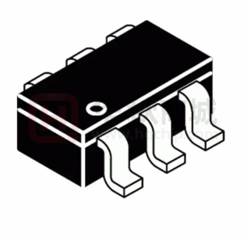
a space-saving 6-pin SOT23 package.
●Wide 3.4V-to-18V Operating Input Range
●100mΩ/80mΩ Low-RDS(ON) Internal Power
MOSFETs
●High-Efficiency Synchronous-Mode Operation
●Fixed 600kHz Switching Frequency
●PFM Mode for High Efficiency at Light Load
●Internal Soft-Start
●Input Voltage UVP&OVP
●Over-Current Protection and Hiccup
●Thermal Shut down
●Output Adjustable from0.6V
●Available in a 6-pin SOT-23 package
APPLICATIONS
●Digital Set-top Box(STB)
●Tablet Personal Computer(Pad)
●Flat-Panel Television and Monitors
●Digital Video Recorder (DVR)
●Portable Media Player(PMP)
●General Purposes
TYPICAL APPLICATIONS
C2
22nF
BS
VIN
VIN
SW
R1
110k
1%
XC8112B
CIN
22μF
XC8112B
Rev.1.05
EN
L
4.7μH
R2
15k
1%
- 1-
C1
22pF
opt.
COUT
22μF
FB
GND
VOUT
�XC8112B
PACKAGE/ORDER INFORMATION
OrderPartNumber
BS
1
6
SW
GND
2
5
VIN
FB
3
4
EN
XC8112B
Package
SOT23-6
FUNCTIONAL PIN DESCRIPTION
PIN
NAME
TYPE
1
BS
I/O
2
GND
G
3
FB
I
4
EN
I
5
VIN
PI
6
SW
I/O
XC8112B
Rev.1.05
FUNCTION DESCRIPTIONS
Boot-Strap Pin. Supply high side gate driver. Decouple this pin to SW
pin with 22nF ceramic cap.
System Ground. Reference ground of the regulated output voltage:
requires extra care during PCB layout. Connect to GND with copper
traces and vias.
Output Feedback Pin. Connect this pin to the center point of the output
resistor divider (as shown in Figure 1) to program the output voltage:
VOUT=0.6×(1+R1/R2)
Pull High to enable the XC8112B. For automatic start
-up, connect EN to
VIN using a 100kΩ resistor. Do not float.
Supply Voltage. The XC8112 B operates from a 3.4V-to-18V input rail.
Requires C1 to decouple the input rail. Connect using a wide PCB
trace.
Switch Output. Connect using a wide PCB trace.
- 2-
�XC8112B
FUNCTION BLOCK DIAGRAM
XC8112B
VIN
+
∑
VCC
REGULATOR
RSEN
-
VCC
CURRENT SENSE
AMPLIFIER
BOOST
REGULATOR
BS
OSCILLATOR
HS
DRIVER
+
COMPARATOR
-
REFERENCE
EN
VCC
SW
ON TIME CONTROL
CURRENT LIMIT
COMPARATOR
1pF
1M
56pF
LOGIC CONTROL
400k
LS
DRIVER
+
+
FB
GND
ERROR AMPLIFIER
ABSOLUTE MAXIMUM RATINGS
PARAMETER
ABSOLUTE MAXIMUM RATINGS
UNIT
VIN,VEN
-0.3 to 20
V
VSW
-0.3 to 20
V
VBS
VSW+6
V
-0.3 to 6
V
Continuous Power Dissipation(TA=+25℃)
1.25
W
Junction Temperature
150
°C
Lead Temperature
260
°C
-65 to150
°C
Thermal Resistance θJA
100
°C/W
Thermal Resistance θJC
55
°C/W
All Other Pins
Storage Temperature
XC8112B
Rev.1.05
-3-
�XC8112B
RECOMMENDED OPERATING CONDITIONS
PARAMETER
RECOMMENDED
Supply Voltage VIN
Output Voltage VOUT
UNIT
3.4 to 18
V
0.6 to 0.9VIN
V
-40 to 125
°C
Operating Junction Temp.(TJ)
ELECTRICAL CHARACTERISTICS
PARAMETER
SYMBOL
TEST
CONDITIONS
MIN
TYP
MAX
UNIT
uA
Supply Current(Shutdown)
IIN
VEN=0V
Supply Current(Quiescent)
Iq
VEN=2V, VFB=1V
0.8
mA
HSS witch-On Resistance
HSRds-on
VBST-SW=5V
100
mΩ
LSS witch-On Resistance
LSRds-on
VCC=5V
80
mΩ
SWLKG
VEN=0V,VSW=12V
Switch Leakage
Current Limit
ILIMIT
Oscillator Frequency
Fsw
VFB=0.75V
Maximum Duty Cycle
DMAX
VFB=700mV
Feedback Voltage
VFB
1
1
3
uA
3.1
A
600
kHz
88
92
%
588
600
612
mV
EN Rising Threshold
VEN_RISING
1.5
V
EN Falling Threshold
VEN_FALLING
1.3
V
VEN=2V
1.6
uA
VEN=0V
0
uA
EN Input Current
VIN UVP Threshold—
Falling
VIN UVP Threshold
Hysteresis
VIN OVP Threshold—
Rising
VIN OVP Threshold
Hysteresis
IEN
VINUVFALL
3.25
3.3
3.35
V
50
mV
19.5
V
50
mV
1
mS
Thermal Shutdown
150
°C
Thermal Hysteresis
20
°C
Soft-Start Period
XC8112B
Rev.1.05
VINOVRISE
TSS
-4-
�XC8112B
TYPICAL PERFORMANCE CHARACTERISTICS
EFFICIENCY VS OUTPUT CURRENT (VOUT=5V)
OUTPUT VOLTAGE VS OUTPUT CURRENT (VOUT=5V)
100%
5.2
90%
5.1
80%
5
OUTPUT VOLTAGE(V)
EFFICIENCY
70%
60%
50%
40%
VIN=12V
30%
VIN=18V
20%
4.9
4.8
4.7
VIN=12V
4.6
VIN=18V
4.5
10%
0%
0
500
1000
1500
2000
4.4
2500
0
OUTPUT CURRENT(mA)
500
1000
STEADY STATE OPERATION
(VIN=12V,VOUT=1.2V,IOUT=100mA)
2000
STEADY STATE OPERATION
(VIN=12V,VOUT=1.2V,IOUT=1000mA)
qw
STRAT UP
(VIN=12V,VOUT=1.2V)
LOAD TRANSIENT RESPONSE
(VIN=12V,VOUT=1.2V,IOUT=100-1000mA,1A/uS)
XC8112B
Rev.1.05
1500
OUTPUT CURRENT(mA)
-5-
2500
�XC8112B
OPERATION
External Components Selection
XC8112B require an input capacitor, an output
capacitor and an��1+
inductor.
These components are
��2
critical to the performance of the device.
XC8112Bare internally compensated and do not
require external components to achieve stable
operation. The output voltage can be programmed
by resistor
= � × divider.
��
�
𝑉𝑂𝑈𝑇 = 𝑉𝐹𝐵
VOUT
R1
COUT
VFB
��2
𝑅1+ 𝑅2
×
𝑅2
R2
Select R1 value around 50kΩ
𝑅2 = 𝑅1×
𝑉𝐹𝐵
𝑉𝑂𝑈𝑇 − 𝑉𝐹𝐵
Where 𝑉𝐹𝐵
as 0.6V
Output Inductorsand
Capacitors Selection
BUCK PowerSupply
Recommendations
There are several design considerations related
to the selection of output inductors and
capacitors:
• Load transient response
• Stability
• E fficiency
• Output ripple voltage
• Over current ruggedness
The device has been optimized for use with
nominal LC values as shown in the Application
Diagram.
XC8112B are designed to operate from input
����( supply range between 3.4V and 18 V.
voltage
This input supply must be well regulated. If the
��
input =supply is located more than a few inches,
additional�� bulk capacitance may be required in
addition to the ceramic bypass capacitors. An
electrolytic capacitor with a value of 47uF is a
typical choice.VIN must be connected to input
capacitors as close as possible.
𝐼𝐿(𝑀𝐴𝑋) = 𝐼𝐿𝑂𝐴𝐷(𝑀𝐴𝑋) + 𝐼𝑅
BUCK Inductor Selection
= 𝐼𝐿𝑂𝐴𝐷(𝑀𝐴𝑋) +
The recommended inductor values are shown in
the Application Diagram. It is important to
guarantee the inductor core does not saturate
during any foreseeable operational situation. The
inductor should be rated to handle the peak load
current plus the ripple current: Care should be
taken when reviewing the different saturation
current ratings that are specified by different
manufacturers. Saturation current ratings are
typically specified at 25°C, so ratings at maximum
ambient temperature of the application should be
requested from the manufacturer.
XC8112B
Rev.1.05
D=
𝐷×( 𝑉𝐼𝑁 − 𝑉𝑂𝑈𝑇 )
2× 𝐿× 𝐹𝑆
𝑉𝑂𝑈𝑇
, 𝐹 = 1.5 𝑀𝐻𝑧, 𝐿 = 2.2 𝑢𝐻
𝑉𝐼𝑁 𝑆
where
• IL(MAX) :Max inductor Current
• ILOAD(MAX) :Max load current
• IR :Peak-to-Peak inductor current
• D :Estimated duty factor
• VIN :Input voltage
• VOUT :Output voltage
• FS :Switching frequency, Hertz
-6-
�Recommended Method for BUCK Inductor Selection
XC8112B
B
The best way to guarantee the inductor does not saturate is to choose an inductor that has saturation current
rating greater than the maximum device current limit , as specified in the Electrical Characteristics . In this case
the device will prevent inductor saturation by going into current limit before the saturation level is reached.
Alternate Method for BUCK Inductor Selection
If the recommended approach cannot be used care must be taken to guarantee that the saturation current is
greater than the peak inductor current:
��
𝐼𝑆𝐴𝑇 > 𝐼𝐿𝑃𝐸𝐴𝐾
𝐼𝐿𝑃𝐸𝐴𝐾 = 𝐼𝑂𝑈𝑇𝑀𝐴𝑋 +
𝐼𝑅 =
𝐷=
𝐼𝑅
2
𝐷 × (𝑉𝐼𝑁 − 𝑉𝑂𝑈𝑇 )
𝐿 × 𝐹𝑆
𝑉𝑂𝑈𝑇
𝑉𝐼𝑁 × 𝐸𝐹𝐹
where
• ISAT:Inductor saturation current at operating temperature
• ILPEAK:Peak inductor current during worst case conditions
• IOUTMAX:Maximum average inductor current
• IR :Peak-to-Peak inductor current
• VOUT:Output voltage
• VIN:Input voltage
• L :Inductor value in Henries at IOUTMAX
• FS:Switching frequency, Hertz
• D :Estimated duty factor
• EFF:Estimated power supply efficiency
ISAT may not be exceeded during any operation, including transients, startup, high temperature, worst case conditions , etc.
Output and Input Capacitors Characteristics
Special attention should be paid when selecting these components. The DC bias of these capacitors can result
in a capacitance value that falls below the minimum value given in the recommended capacitor specifications
table.The ceramic capacitor’s actual capacitance can vary with temperature. The capacitor type X7R, which
operates over a temperature range of −55°C to +125°C, will only vary the capacitance to within ±15%. The
capacitor type X5R has a similar tolerance over a reduced temperature range of −55°C to +85°C. Many large
value ceramic capacitors, larger than 1uF are manufactured with Z5U or Y5V temperature characteristics. Their
capacitance can drop by more than 50% as the temperature varies from 25°C to 85°C. Therefore X5R or X7R
is recommended over Z5U and Y5V in applications where the ambient temperature will change significantly
above or below 25°C.Tantalum capacitors are less desirable than ceramic for use as output capacitors because
they are more expensive when comparing equivalent capacitance and voltage ratings in the 0.47uF to 44uF
range. Another important consideration is that tantalum capacitors have higher ESR values than equivalent
size ceramics. This means that while it may be possible to find a tantalum capacitor with an ESR value within the stable
range, it would have to be larger in capacitance (which means bigger and more costly) than a ceramic capacitor with the
same ESR value. It should also be noted that the ESR of a typical tantalum will increase about 2:1 as the temperature goes
from 25°C down to −40°C, so some guard band must be allowed .
BUCK Output Capacitor Selection
TheoutputcapacitorofaswitchingconverterabsorbstheACripplecurrentfromtheinductorandprovidestheinitialresponsetoa
The output capacitor of a switching converter absorbs the AC ripple current from the inductor and provides the
loadtransient.Theripplevoltageattheoutputoftheconverteristhe
productoftheripplecurrentflowingthroughtheoutput
initial response to a load transient. The ripple voltage
at the output of the converter is the product of the ripple
capacitorandtheimpedanceofthecapacitor.Theimpedanceofthecapacitorcanbedominatedbycapacitive,resistive,or inductiveelements
current flowing through the output capacitor and the impedance of the capacitor. The impedance of the
capacitor can be dominated by capacitive, resistive, or inductive elements within the capacitor, depending
on
andremaincapacitiveuptohighfrequencies.Theirinductivecomponentcanbeusuallyneglectedatthefrequencyrangesthe
switcheroperates.
the frequency
of the ripple current.
Ceramic
capacitors totheloadandhelpsmaintain
have very low ESR and
remain capacitive
up to high
Theoutput-filter
capacitorsmoothes
outthecurrent
flowfromtheinductor
asteadyoutput
voltage duringtransient
loadchanges.
Italsoreduces
outputvoltagecomponent
ripple.Thesecapacitors
with
frequencies
. Their inductive
can be mustbeselected
usually neglected
at the frequency ranges the switcher
sufficientcapacitanceandlowenoughESRtoperformthesefunctions.
operates .The output-filter capacitor smoothes out the current flow from the inductor to the load and helps
NotethattheoutputvoltagerippleincreaseswiththeinductorcurrentrippleandtheEquivalentSeriesResistanceoftheoutput
maintain a steady output voltage during transient load changes. It also reduces output voltage ripple. These
capacitor(ESRCOUT ).Alsonotethattheactualvalueofthecapacitor’sESRCOUTisfrequencyandtemperaturedependent,as
capacitors must be selected with sufficient capacitance and low enough ESR to perform these functions. Note
specifiedbyitsmanufacturer.TheESRshouldbecalculatedattheapplicableswitchingfrequencyand
that the output voltage ripple increases with the inductor current ripple and the Equivalent Series Resistance of
ambienttemperature.
the output capacitor (ESRCOUT).Also note that the actual value of the capacitor’s ESRCOUT is frequency and
temperature dependent, as specified by its manufacturer. The ESR should be calculated at the applicable
switching frequency and ambient temperature.
withinthecapacitor, depending onthefrequency oftheripple current. Ceramic capacitors haveverylowESR
XC8112B
Rev.1.05
-7-
�XC8112B
B
BUCK Output Capacitor Selection
𝑉𝑂𝑈𝑇−𝑅 − 𝑃𝑃 =
where
𝐼𝑅
8 × 𝐹𝑆 × 𝐶𝑂𝑈𝑇
Output ripple can be estimated from the vector sum
of the reactive (capacitance ) voltage component and
2
+�� 2 component of the output
the real (ESR) voltage
2
2
+ 𝑉𝐶𝑂𝑈𝑇
VOUT-R-PP = �𝑉𝑅𝑂𝑈𝑇
𝐷 × (𝑉𝐼𝑁 − 𝑉𝑂𝑈𝑇 )
2 × 𝐿 × 𝐹𝑆
𝑉𝑂𝑈𝑇
𝐷=
𝑉𝐼𝑁
𝐼𝑅 =
where
𝑉𝑅𝑂𝑈𝑇 = 𝐼𝑅 × 𝐸𝑆𝑅𝐶𝑂𝑈𝑇
𝑉𝐶𝑂𝑈𝑇 =
where
• VOUT-R -PP:estimated output ripple,
• IR :estimated current ripple
• D:Estimated duty factor
𝐼𝑅
8 × 𝐹𝑆 × 𝐶𝑂𝑈𝑇
where
• VOUT-R -PP:estimated output ripple,
• VROUT:estimated real output ripple,
• VCOUT:estimated reactive output ripple.
The device is designed to be used with ceramic capacitors on the outputs of the buck regulators. The
recommended dielectric type of these capacitors is X5R, X7R, or of comparable material to maintain
proper tolerances over voltage and temperature. The recommended value for the output capacitors is 22µF,
6.3V with an ESR of 2mΩ or less. The output capacitors need to mounted as close as possible to the
output/ground terminals of the device.
BUCK Input Capacitor Selection
input capacitor should be located as close as possible to
their corresponding VIN and GND terminals, tantalum ��
capacitor can also be located in the proximity of the
�𝑉𝑂𝑈𝑇 × (𝑉𝐼𝑁 − 𝑉𝑂𝑈𝑇 )
device.The input capacitor supplies the AC switching current 𝑉𝑅𝑀𝑆_𝐶𝐼𝑁 = 𝐼𝑂𝑈𝑇
𝑉𝑂𝑈𝑇
drawn from the switching action of the internal power
MOSFETs. The input current of a buck converter is The power dissipated in the input capacitor is given by:
discontinuous , so the ripple current supplied by the input
2
× 𝑅𝐸𝑆𝑅_𝐶𝐼𝑁
𝑃𝐷_𝐶𝐼𝑁 = 𝐼𝑅𝑀𝑆_𝐶𝐼𝑁
capacitor is large. The input capacitor must be rated to hand
le both the RMS current and the dissipated power. The input
capacitor must be rated to handle this current:
The device is designed to be used with ceramic capacitors on
the inputs of the buck regulators. The recommended
dielectric type of these capacitors is X5 R, X7R, or of
comparable material to maintain proper tolerances over
voltage and temperature. The minimum recommended
value for the input capacitor is 10µF with a n ESR of 10mΩ
or less. The input capacitors need to be mounted as close as
possible to the power/ground input terminals of the device
The input power source supplies the average current
continuously. During the high side MOSFET switch on-time,
however, the demanded di/dt is higher than can be typically
supplied by the input power source. This delta is supplied by
the input capacitor A simplified “worst case” assumption
is that all of the high side MOSFET current is supplied by the
input capacitor. This w ill Result in conservative estimates of
input ripple voltage and capacitor RMS Current. Input ripple
voltage is estimated as besides:
XC8112B
Rev.1.05
-8-
��
𝑉𝑃𝑃𝐼𝑁 =
where
𝐼𝑂𝑈𝑇 × 𝐷
+ 𝐼𝑂𝑈𝑇 × 𝐸𝑆𝑅𝐶𝐼𝑁
𝐶𝐼𝑁 × 𝐹𝑆
• VPPIN:Estimated peak-to-peak input ripple voltage
• IOUT :Output current
• CIN:Input capacitor value
• ESRCIN :Input capacitor ESR
�XC8112B
B
BUCK Input Capacitor Selection
This capacitor is exposed to significant RMS current, so
it is important to select a capacitor with an adequate
RMS current rating. Capacitor RMS current estimated
as besides:
2
𝐼𝑅𝑀𝑆𝐶𝐼𝑁 = �𝐷 × (𝐼𝑂𝑈𝑇
+
2
𝐼𝑅𝐼𝑃𝑃𝐿𝐸
)
12
Where
•IRMSCIN :Estimated input capacitor RMS current
PCBOARD LAYOUT
PC board layout is an important part of DC-DC converter design. Poor board layout can disrupt the
performance of a DC- DC converter and surrounding circuitry by contributing to EMI, ground bounce, and
resistive voltage loss in the traces. These can send erroneous signals to the DC-DC converter resulting in poor
regulation or instability. Good layout can be implemented b y following a few simple design rules .
1. Minimize area of switched current loops. In a buck
regulator there are two loops where currents are
switched rapidly. The first loop starts from the CIN input
capacitor, to the regulator VIN terminal, to the regulator
SW terminal, to the inductor then out to the output
capacitor COUT and load. The second loop starts from
the output capacitor ground , to the regulator GND
terminals, to the inductor and then out to COUT an d
the load. To minimize both loop area s the input
capacitor should be placed as close as possible to the
VIN terminal. Grounding for both the input and output
capacitors should consist of a small localized top side
plane that connects to GND. The inductor should be
placed as close as possible to the SW pin and output
capacitor.
3. Have a single point ground for all device analog g
rounds . The ground connections for the feedback
1.Minimize areaofswitched currentloops.Inabuckregulator the
components
should be connected together firstloop
then
-rearetwoloopswherecurrentsareswitchedrapidly.The
routed
to
the
GND
pin
of
the
dev
ice.
This
prevents
startsfromtheCINinputcapacitor,totheregulatorVINterminal, any
totheregulatorSWterminal,totheinductorthenouttotheout
switched
or load currents from flowing in the analog
loopstartspoor
fromthe
-putcapacitor
COUT andload.Thesecond
ground
plane.
If not properly handled,
grounding
outputcapacitorground,totheregulatorGNDterminals,tothe
can
result
in
degraded
load
regulation
or
erratic
inductorandthenouttoCOUT andtheload.Tominimize bothloop
switching
behavior.
areastheinputcapacitorshouldbeplacedascloseaspossibleto
theVINterminal.Groundingforboththeinputandoutputcapacitors
shouldconsistofasmalllocalizedtopsideplanethatconnectsto
GND.Theinductorshouldbeplacedascloseaspossibletothe
SWpinandoutputcapacitor.
3.Haveasinglepointground foralldeviceanaloggrounds.
Thegroundconnectionsforthefeedbackcomponents
shouldbeconnectedtogetherthenroutedtotheGNDpin
ofthedevice.Thispreventsanyswitchedorloadcurrents
fromflowingintheanaloggroundplane.Ifnotproperly
handled,poorgroundingcanresultindegradedloadregul
XC8112B
Rev.1.05
-9-
2. Minimize the copper area of the switch node.
The SW terminals should be directly connected
with a trace that runs on top side directly to the
inductor. To minimize IR losses this trace should
be as short as possible and with a sufficient width
. However, a trace that is wider than 100 mils will
increase the copper area and cause too much
capacitive loading on the SW terminal. The
inductors should be placed as close as possible
to the SW terminals to further minimize the copper
area of the switch node.
4. Minimize trace length to the FB terminal. The
feedback trace should be routed away from the
SW pin and inductor to avoid contaminating the
feedback signal with switch noise.
5. Make input and output bus connections as wide
as possible. This reduces any voltage drop s o n
the input or output of the converter and can
improve efficiency. If voltage accuracy at the load
is important make sure feedback voltage sense is
made at the load. Doing so will correct for voltage
drop s at the load and provide the best output
accuracy.
�XC8112B
B
PACKAGE
SOT23-6
2.80
3.00
0.95
BSC
0.60
TYP
1.20
TYP
EXAMPLE
TOP MARK
AAAA
1.50
1.70
2.60
TYP
2.60
3.00
PIN 1
RECOMMENDED SOLDER PAD
LAYOUT
TOP VIEW
GAUGE PLANE
0.25 BSC
0.90
1.30
1.45 MAX
SEATING PLANE
0.30
0.50
0.95 BSC
0.00
0.15
0°~8°
FRONT VIEW
SIDE VIEW
NOTE:
1.DIMENSIONS ARE IN MILLIMETERS.
2.DRAWING NOT TO SCALE.
3.DIMENSIONS ARE INCLUSIVE OF PLATING.
4.DIMENSIONS ARE EXCLUSIVE OF MOLD FLASH AND METAL BURR.
XC8112B
Rev.1.05
0.30
0.55
- 10-
0.09
0.20
�