SunlordBusiness categories:Level 0(general confidential) Specifications for Wire Molded SMD Power Inductors Page 1 of 18
for Automotive Electronics
S P E C I F I C AT I O N S
Customer
Product Name
Wire Wound Molded SMD Power Inductors
Sunlord Part Number
AMWSA -S Series
Customer Part Number
[
New Released,
Revised]
SPEC No.: AMWSA03210000
【This SPEC is total 18 pages including specifications and appendix.】
【ROHS, Halogen-Free and SVHC Compliant Parts】
Approved By
Checked By
Issued By
Shenzhen Sunlord Electronics Co., Ltd.
Address: Sunlord Industrial Park, Dafuyuan Industrial Zone, Guanlan, Shenzhen, China 518110
Tel: 0086-755-29832333
Fax: 0086-755-82269029
E-Mail: sunlord@sunlordinc.com
【For Customer approval Only】
Qualification Status:
Full
Approved By
Verified By
Comments:
Date:
Restricted
Rejected
Re-checked By
Checked By
�SunlordBusiness categories:Level 0(general confidential) Specifications for Wire Molded SMD Power Inductors Page 2 of 18
【Version change history】
Rev.
Effective Date
Changed Contents
Change Reasons
Approved By
01
/
New release
/
Simei Yu
�SunlordBusiness categories:Level 0(general confidential) Specifications for Wire Molded SMD Power Inductors Page 3 of 18
Caution:
All products listed in this specification are developed, designed and intended for use in general electronics equipment. The products are not
designed or warranted to meet the requirements of the applications listed below, whose performance and/or quality require especially high
reliability, or whose failure, malfunction or trouble might directly cause damage to society, person, or property. Please understand that we are
not responsible for any damage or liability caused by use of the products in any of the applications below. Please contact us for more details if
you intend to use our products in the following applications.
1.
Aircraft equipment
2.
Aerospace equipment
3.
Undersea equipment
4.
nuclear control equipment
5.
military equipment
6.
Power plant equipment
7.
Medical equipment
8.
Transportation equipment (automobiles, trains, ships,etc.)
9.
Traffic signal equipment
10. Disaster prevention / crime prevention equipment
11. Data-processing equipment
12. Applications of similar complexity or with reliability requirements comparable to the applications listed in the above
�SunlordBusiness categories:Level 0(general confidential) Specifications for Wire Molded SMD Power Inductors Page 4 of 18
1.
2.
Scope
This specification applies to AMWSA series of wire wound molded SMD power Inductors
Product Description and Identification (Part Number)
1)
Description
Wire Wound Molded SMD Type Power Inductor.
2)
Product Identification (Part Number)
AMWSA XXXX
-XXX
□
T
XXX
①
②
③
④
⑤
⑥
①
Type
AMWSA
③
②
External Dimensions (mm)
Wire wound molded SMD power
Inductors
0412S~1707S
Nominal Inductance
Example
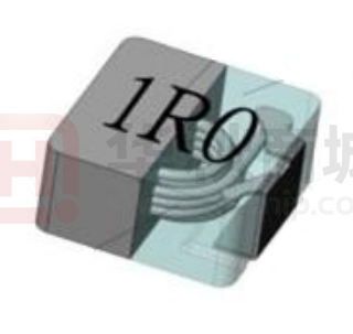
1R0
1.0μH
100
10μH
101
100μH
⑥
④
Nominal Value
Inductance Tolerance
M
±20%
N
±30%
⑤
Packing
T
Tape Carrier Package
Special code
XXX
3.
4.
Electrical Characteristics
Please refer to Appendix A.
1)
Operating temperature range (Including self-heating): -55℃~+155℃.
2)
Storage temperature and humidity range (product with tapping ): -10℃~+40℃, RH 70% Max.
Shape and Dimensions
1)
Dimensions and recommended PCB pattern for reflow soldering: See Fig.4-1 and Table 4-1.
Unit: mm
Series
A
B
C
D
E
I Typ.
J Typ.
H Typ.
AMWSA0412S
4.2±0.25
4.4±0.35
1.0±0.2
0.8±0.3
2.0±0.3
1.5
2.2
2.5
AMWSA0402S
4.2±0.25
4.4±0.35
1.8±0.2
0.8±0.3
2.0±0.3
1.5
2.2
2.5
AMWSA0518S
5.2±0.2
5.4±0.35
1.6±0.2
1.20±0.2
2.2±0.3
1.9
2.2
2.5
AMWSA0503S
5.2±0.2
5.4±0.35
2.8±0.2
1.20±0.2
2.2±0.3
1.9
2.2
2.5
AMWSA0618S
6.6±0.2
7.0±0.3
1.6±0.2
1.60±0.3
3.0±0.3
2.35
3.7
3.5
AMWSA0602S
6.6±0.2
7.0±0.3
1.8±0.2
1.60±0.3
3.0±0.3
2.35
3.7
3.5
AMWSA0624S
6.6±0.2
7.0±0.3
2.2±0.2
1.60±0.3
3.0±0.3
2.35
3.7
3.5
AMWSA0603S
6.6±0.2
7.0±0.3
2.8±0.2
1.60±0.3
3.0±0.3
2.35
3.7
3.5
AMWSA0604S
6.6±0.2
7.0±0.3
3.8±0.2
1.60±0.3
3.0±0.3
2.35
3.7
3.5
AMWSA0605S
6.6±0.2
7.0±0.3
4.8±0.2
1.60±0.3
3.0±0.3
2.35
3.7
3.5
AMWSA1003S
10.0±0.3
11.5 Max
2.8±0.2
2.0±0.5
3.0±0.3
4.1
5.4
4.1
AMWSA1004S
10.0±0.3
11.0±0.5
3.8±0.2
2.0±0.5
3.0±0.5
4.1
5.4
4.1
AMWSA1005S
10.0±0.3
11.5 Max
4.8±0.2
2.0±0.5
3.0±0.5
4.1
5.4
4.1
AMWSA1204S
12.8±0.5
13.45±0.35
4.0Max.
2.0±0.5
See Remarks
3.25
8.0
5.5
AMWSA1205S
12.6±0.3
13.45±0.35
4.8±0.2
2.0±0.5
See Remarks
3.25
8.0
5.5
AMWSA1206S
12.6±0.3
13.45±0.35
5.8±0.2
2.0±0.5
See Remarks
3.25
8.0
5.5
�SunlordBusiness categories:Level 0(general confidential) Specifications for Wire Molded SMD Power Inductors Page 5 of 18
AMWSA1265S
12.6±0.3
13.45±0.35
6.5Max.
2.0±0.5
5.0±0.3
3.25
8.0
5.5
AMWSA1707S
17.15Max
17.15±0.35
7.0Max
2.5±0.5
12.0±0.3
3.50
11.2
12.8
Remarks:
Series
E(mm)
Dimensions
3.85±0.5
R22/R47
5.0±0.3
R68/R82/1R0/1R5/2R2/3R3/4R7/6R8/100/150/220
3.85±0.5
R22/R36/R50/R68/R82/1R0/1R5/2R2
5.0±0.3
3R3/4R7/6R8/100/150/220/330/470
3.85±0.5
1R5/2R2
5.0±0.3
3R3/4R7/5R6/6R8/8R2/100/120/150/180/220/270/330/470/680/101/121/151
AMWSA1204S
AMWSA1205S
AMWSA1206S
Structure and Components: See Table 4-2
[
Table 4-2
Components
Material
INK
Ink(black)
CORE
Alloy Sponge Powder
WIRE
Polyurethane copper wire
BASE
Copper plated with Sn
Thickness of BASE coating:See Table 4-3
[
Table 4-3
5.
Coating material
Thickness (μm)
Nickel bottom
0.125~0.625
Tin layer
5~7
Test and Measurement Procedures
5.1 Test Conditions
5.1.1 Unless otherwise specified, the standard atmospheric conditions for measurement/test as:
a. Ambient Temperature: 20±15℃
b. Relative Humidity: 65±20%
c. Air Pressure: 86 KPa to 106 KPa
5.1.2 If any doubt on the results, measurements/tests should be made within the following limits:
a. Ambient Temperature: 20±2℃
b. Relative Humidity: 65±5%
c. Air Pressure: 86KPa to 106 KPa
5.2 Visual Examination
a. Inspection Equipment: 10 X magnifier
5.3 Electrical Test
5.3.1 DC Resistance (DCR)
a. Refer to Appendix A.
b. Test equipment (Analyzer): HIOKI3540 or equivalent.
5.3.2 Inductance (L)
a. Refer to Appendix A.
b. Test equipment: Wayne kerr3260+3265B or equivalent.
5.3.3 Rated Current
a. Refer to Appendix A.
b. Test equipment: Wayne kerr3260+3265B, Agilent E3633A, R2M-2H3 or equivalent.
c. Definition of Rated Current (Ir): With the condition of the DC current pass, the inductance decrease approximate 30% of
the standard value, compare to the temperature rise approximate 40℃, the smaller is Rated Current.(reference
environment temperature:20℃)
5.4 Reliability Test
�SunlordBusiness categories:Level 0(general confidential) Specifications for Wire Molded SMD Power Inductors Page 6 of 18
Mechanical Reliability
Item
Solderability
Specification and Requirement
Test Method
The surface of terminal immersed shall be
Solder heat proof:
minimum of 95% covered with a new coating of
1.
Preheating: 160 ± 10 ℃
solder
2.
Retention time: 245 ± 5 ℃ for 2 ± 0.5 seconds
1.
Vibration frequency:
(10 Hz to 55 Hz to 10Hz) in 60 seconds as a period
Inductance
change:
Within
± 10%
Without
2.
Vibration time:
Vibration
mechanical damage such as break
Period cycled for 2 hours in each of 3 mutual perpendicular
directions.
Inductance
change:
Within
± 10%
Without
3.
Amplitude: 1.5 mm max.
1.
Peak value: 100 G
2.
Duration of pulse: 11ms
3.
3 times in each positive and negative direction of 3 mutual
Shock
mechanical damage such as break
perpendicular directions
Insulating
Over 100MΩ
4.
Over 100MΩ at 100V D.C. between coil and core
Resistance
Endurance Reliability
Item
Specification and Requirement
Test Method
1.
Repeat 100 cycles as follow:
(-55 ± 2 ℃; 30 ± 3 min)
→(Room temp., 5 min)
Inductance change: Within ± 10% Without distinct
→ (+155 ± 2 ℃, 30 ± 3 min)
Thermal Shock
damage in appearance
→ (Room temp., 5 min)
2.
Recovery: 48 + 4 / -0 hours of recovery under the standard
condition after the test.
1.
High Temperature
Environment condition: 85 ± 2 ℃
Inductance change: Within ± 10% Without distinct
Applied Current: Rated current
Resistance
Humidity
Resistance
damage in appearance
2.
Duration: 1000 + 4 / -0 hours
1.
Environment condition: 60 ± 2 ℃
Inductance change: Within ±10% Without distinct
Humidity: 90–95%
damage in appearance
Applied Current: Rated current
2.
Low Temperature
Store
High Temperature
Store
6.
Duration: 1000 + 4 / -0 hours
Inductance change: Within ± 10% Without distinct
Store temperature:
damage in appearance
-55 ± 2 ℃,1000 + 4 / -0 hours
Inductance change: Within ± 10% Without distinct
Store temperature:
damage in appearance
+155 ± 2 ℃,1000 + 4 / -0 hours
Packaging, Storage and Transportation
6.1 Tape Carrier Packaging:
Packaging code: T
(1) Tape carrier packaging are specified in attached figure Fig.6.1-1~2
(2) Tape carrier packaging quantity:
Type
Standard Quantity
(pcs/reel)
Type
Standard Quantity
(pcs/reel)
�SunlordBusiness categories:Level 0(general confidential) Specifications for Wire Molded SMD Power Inductors Page 7 of 18
AMWSA0412S
AMWSA0402S
AMWSA0518S
AMWSA0503S
AMWSA0618S
3000
AMWSA0603S
1500
3000
AMWSA0604S
1000
2000
AMWSA0605S
1000
2000
AMWSA1004S
500
500
1500
AMWSA1204S
AMWSA0602S
1500
AMWSA1205S
500
AMWSA0624S
1500
AMWSA1206S
500
AMWSA1265S
500
AMWSA1707S
200
AMWSA1003S
800
AMWSA1005S
500
a. Taping Drawings (Unit: mm)
Fig.6.1-1
b.Reel and Taping Dimensions (Unit: mm)
Fig.6.1-2
Remark:
(AMWSA0412S- AMWSA1265S)- Fig.6.1-1/2
Fig.6.1-3
Remark:
(AMWSA1707S) -Fig.6.1-3
�SunlordBusiness categories:Level 0(general confidential) Specifications for Wire Molded SMD Power Inductors Page 8 of 18
Reel dimensions (mm)
Tape dimensions (mm)
Type
A
N
C
W
W0
P
P0
H
T
A0
B0
AMWSA0412S
330±2.0 100±2.0 13±1.0
12.4±
2.0
12±0.3
8±0.1
4±0.1
1.5±
0.05
0.30±
0.05
4.4±0.1 4.9±0.1
AMWSA0402S
330±2.0 100±2.0 13±1.0
12.4±
2.0
12±0.3
8±0.1
4±0.1
2.3±
0.05
0.35±
0.05
4.4±0.1 4.9±0.1
AMWSA0518S
330±2.0 100±2.0 13±1.0
12.4±
2.0
12±0.3
8±0.1
4±0.1
2.1±
0.05
0.35±
0.05
5.4±0.1 5.9±0.1
AMWSA0503S
330±2.0 100±2.0 13±1.0
12.4±
2.0
12±0.3
8±0.1
4±0.1
3.3±
0.05
0.35±
0.05
5.4±0.1 5.9±0.1
AMWSA0618S
330±2.0 100±2.0 13±1.0
16.4±
2.0
16±0.3
12±0.1
4±0.1
2.1±
0.05
0.35±
0.05
6.9±0.1 7.5±0.1
AMWSA0602S
330±2.0 100±2.0 13±1.0
16.4±
2.0
16±0.3
12±0.1
4±0.1
2.2±0.1
0.35±
0.05
6.9±0.1 7.5±0.1
AMWSA0624S
330±2.0 100±2.0 13±1.0
16.4±
2.0
16±0.3
12±0.1
4±0.1
2.7±
0.05
0.35±
0.05
6.9±0.1 7.5±0.1
AMWSA0603S
330±2.0 100±2.0 13±1.0
16.4±
2.0
16±0.3
12±0.1
4±0.1
3.3±
0.05
0.35±
0.05
6.9±0.1 7.5±0.1
AMWSA0604S
330±2.0 97±0.5
13.2±
0.2
16.8±
2.0
16±0.3
12±0.1
4±0.1
4.2±
0.10
0.35±
0.05
6.9±0.1 7.5±0.1
AMWSA0605S
330±2.0 100±2.0 13±1.0
16.4±
2.0
16±0.3
12±0.1
4±0.1
5.2±
0.10
0.4±
0.05
6.9±0.1 7.5±0.1
AMWSA1003S
330±2.0 100±2.0 13±1.0
24.4±
2.0
24±0.3
16±0.1
4±0.1
3.3±
0.10
0.35±
0.05
10.4±
0.1
11.6±
0.1
AMWSA1004S
330±2.0 100±2.0 13±1.0
24.4±
2.0
24±0.3
16±0.1
4±0.1
4.3±
0.10
0.35±
0.05
10.4±
0.1
11.5±
0.1
AMWSA1204S
330±2.0 100±2.0 13±1.0
24.4±
2.0
24±0.3
16±0.1
4±0.1
4.3±
0.10
0.5±
0.05
13.4±
0.1
14.4±
0.1
AMWSA1005S
330±2.0 100±2.0 13±1.0
24.4±
2.0
24±0.3
16±0.1
4±0.1
5.4±
0.10
0.5±
0.05
10.4±
0.1
11.6±
0.1
AMWSA1205S
330±2.0 100±2.0 13±1.0
24.4±
2.0
24±0.3
16±0.1
4±0.1
5.3±
0.10
0.5±
0.05
13.2±
0.1
14.4±
0.1
AMWSA1206S
330±2.0 100±2.0 13±1.0
24.4±
2.0
24±0.3
16±0.1
4±0.1
6.3±
0.10
0.5±
0.05
13.2±
0.1
14.4±
0.1
AMWSA1265S
330±2.0 97±0.5
13±0.2
24.0±
0.5
24±0.3
16±0.1
4±0.1
6.8±
0.10
0.5±
0.05
13.1±
0.1
14.0±
0.1
AMWSA1707S
330±2.0 97±0.5
13±0.2
24.4±
2.0
32±0.3
24±0.1
4±0.1
7.3±
0.10
0.5±
0.05
17.5±
0.1
18.1±
0.1
c.Peeling off force: 10gf to 130gf in the direction show below.
Top tape or cover tape
1650~ 1800
Base tape
Fig. 6.1-4
6.2 Storage
(1) The solderability of the external electrodes may deteriorate if packages are stored in high humidity. Besides, to ensure packing
material’s good state, packages must be stored at -10℃ to 40℃ and 70% RH Max.
(2) The solderability of the external electrodes may deteriorate if packages are exposed to dust of harmful gas (e.g. HCl, sulfurous gas of
H2S).
(3) Packaging materials may deform if packages are exposed directly to sunlight.
(4) Minimum packages, such as polyvinyl heat-seal packages shall not be opened until they are used. If opened, use the reels as soon
as possible.
(5) Solderability shall be guaranteed for a period of time from the date of delivery on condition that they are stored at the specified
environment. For those parts, which passed more than the time shall be checked solderability before using.
(6) For magnetic products, keep clear of anything that may generate magnetic fields to avoid change of products performance.
(7) To avoid any damage to products, do not load mechanic force on products or place heavy goods on products, and exclude strong
vibration or drop.
(8)In case of storage over 12 months, solderability shall be checked before actual usage.
�SunlordBusiness categories:Level 0(general confidential) Specifications for Wire Molded SMD Power Inductors Page 9 of 18
7.
Warning and Attentions
7.1 Precautions on Use
(1) Always wear static control bands to protect against ESD.
(2) Any devices used with the products (soldering irons, measuring instruments) should be properly grounded.
(3) Keep bare hands and metal conductors (i.e., metal desk) away from electrodes or conductive areas that lead to electrodes.
(4) Preheat when soldering.
(5) Don’t apply current in excess of the rated current value. It may reduce the impedance or inductance, or cause damage to
components due to over-current.
(6) For magnetic products, keep clear of anything that may generate magnetic fields such as speakers and coils. Use non-magnetic
tweezers when handing the chips.
(7) When soldering, the electrical characteristics may be varied due to hot energy and mechanical stress.
(8) When coating products with resin, the relatively high resin curing stress may change the electrical characteristics. For exterior
coating, select resin carefully so that electrical and mechanical performance of the product is not affected. Before using, please
evaluate reliability with the product mounted in your application set.
(9) When mount chips with adhesive in preliminary assembly, do appropriate check before the soldering stage, i.e., the size of land
pattern, type of adhesive, amount applied, hardening of the adhesive on proper usage and amounts of adhesive to use.
(10) Mounting density: Add special attention to radiating heat of products when mounting other components nearby. The excessive heat
by other products may cause deterioration at joint of this product with substrate.
(11) Since some products are constructed like an open magnetic circuit, narrow spacing between components may cause magnetic
coupling.
(12) Please do not give the product any excessive mechanical shocks in transportation.
(13) Please do not touch wires by sharp terminals such as tweezers to avoid causing any damage to wires.
(14) Please do not add any shock and power to the soldered product to avoid causing any damage to chip body.
(15) Please do not touch the electrodes by naked hand as the solderability of the external electrodes may deteriorate by grease or oil on
the skin.
7.2 PCB Bending Design
The following shall be considered when designing and laying out PCB’s.
(1) PCB shall be designed so that products are not subjected to the mechanical stress from board warp or deflection.
Products shall be located in
the sideways direction to
the mechanical stress
(Poor example)
(Good example)
(2) Products location on PCB separation.
C
Seam
A
B
Product shall be located carefully because they may
be subjected to the mechanical stress in order of A>C=B>D.
D
(3) When splitting the PCB board, or insert (remove) connector, or fasten thread after mounting components, care is required so as not to
give any stress of deflection or twisting to the board. Because mechanical force may cause deterioration of the bonding strength of
electrode and solder, even crack of product body. Board separation should not be done manually, but by using appropriate devices.
7.3 Recommended PCB Design for SMT Land-Patterns
When chips are mounted on a PCB, the amount of solder used (size of fillet) can directly affect chip performance. Therefore, the following
items must be carefully considered in the design of solder land patterns:
(1) The amount of solder applied can affect the ability of chips to withstand mechanical stresses which may lead to breaking or cracking.
Therefore, when designing land-patterns it is necessary to consider the appropriate size and configuration of the solder pads which in
turn determines the amount of solder necessary to form the fillets.
(2) When more than one part is jointly soldered onto the same land or pad, the pad must be designed that each component’s soldering
point is separated by solder-resist.
Recommended land dimensions please refer to product specification.
8
Recommended Soldering Technologies
8.1Re-flowing Profile:
△ Preheat condition: 150 ~200℃/60~120sec.
△ Allowed time above 217℃: 60~90sec.
△ Max temp: 260℃
△ Max time at max temp: 10sec.
△ Solder paste: Sn/3.0Ag/0.5Cu
△ Allowed Reflow time: 2x max
Please refer to Fig. 8.1
[Note: The reflow profile in the above table is only for
qualification and is not meant to specify board assembly
Peak 260℃ max
260℃
Max Ramp Up Rate=3℃/sec.
217℃
Max Ramp Down Rate=6℃/sec.
60~90sec.
200℃
150℃
60~120sec.
25℃
Time 25℃ to Peak =8 min max
Fig. 8.1
�SunlordBusiness categories:Level 0(general confidential) Specifications for Wire Molded SMD Power Inductors Page 10 of 18
profiles. Actual board assembly profiles must be based on
the customer's specific board design, solder paste and process,
and should not exceed the parameters as the Reflow profile shows.]
8.2 Iron Soldering Profile
△ Iron soldering power: Max. 30W
△ Pre-heating: 150℃/60sec.
350℃
△ Soldering Tip temperature: 350℃ Max.
3sec. Max.
Soldering Iron
△
△
△
Soldering time: 3sec. Max.
Solder paste: Sn/3.0Ag/0.5Cu
Max.1 times for iron soldering
Please refer to Fig. 8.2.
[Note: Take care not to apply the tip of
Tc ℃
the soldering iron to the terminal electrodes.]
8.3 Recommended Soldering Technologies
Heat Gun Profile
△ Soldering tip temperature: 350℃ Max.
△ Hot air time: