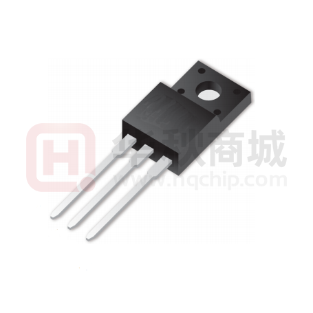
MS8N100FE/FK/FS/FT
Features
Low gate charge
Low Crss (typ 9pF)
Fast switchin
100% avalanche tested
Improved dv/dt capability
RoHS product
Applications
High frequency switching mode power supply
Electronic ballast
UPS
Absolute Ratings (Tc=25℃)
Parameter
Symbol
Value
Unit
Drain-Source Voltage
VDSS
1000
V
Drain Current-continuous
ID T=25℃
T=100℃
8
A
5
A
Drain Current-pulse
(note 1)
IDM
32*
A
Gate-Source Voltage
VGS
±30
V
Single pulse avalanche
energy(note 2)
EAS
650
mJ
Avalanche Current(note 1)
IAR
8
A
Repetitive Avalanche
Energy(note 1)
EAR
16.7
mJ
Power Dissipation
(TO-263\TO-262\TO-220)
PD
TC=25℃
Derate above
25℃
167
W
1.43
W/℃
Power Dissipation
(TO-220F)
PD
TC=25℃
Derate above
25℃
31.7
W
0.25
W/℃
Operating and Storage
Temperature Range
TJ,TSTG
-55~+150
℃
dv/dt
4.5
V/ns
TL
300
℃
Peak Diode Recovery dv/dt
(note 3)
Maximum Lead Temperature
for Soldering Purposes
*Drain current limited by maximum junction temperature
H1.05
Maspower
1
�MS8N100FE/FK/FS/FT
Electrical Characteristics(TCASE=25℃
Parameter
Drain-Source Voltage
Breakdown Voltage
Temperature Coefficient
unless otherwise specified)
Symbol Tests conditions
BVDSS
ID=250μA,VGS=0V
Min Type Max Units
1000
-
-
V
∆BVDSS/∆ ID=250μA,referenced
TJ
to 25℃
-
1.05
-
V/℃
VDS=1000V,VGS=0V,
TC=25℃
-
-
1
μA
VDS=800V,TC =125℃
-
-
10
μA
Zero Gate Voltage Drain
Current
IDSS
Gate body leakage
current
IGSS
VDS=0V,VGS=±30V
-
-
±100
nA
Gate Threshold Voltage
VGS(th)
VDS=VGS,ID=250μA
3.0
-
5.0
V
Static Drain-Source
On-Resistance
RDS(ON)
VGS=10V,ID=4A
-
1.8
2
Ω
Forward
Transconductance
gFS
VDS=40V,ID=4A
(note 4)
-
5.6
-
S
On-Characteristics
Dynamic Characteristics
Input capacitance
Ciss
Output capacitance
Coss
Reverse transfer
capacitance
Crss
VDS=25V,
VGS=0V,
f=1.0MHZ
Electrical Characteristics(TCASE=25℃
Parameter
-
1320 1716
pF
-
105
136
pF
-
9
12
pF
unless otherwise specified)
Symbol Tests conditions Min Type Max Units
Switching-Characteristics
Turn-On delay time
td(on)
Turn-On rise time
tr
Turn-Off delay time
td(Off)
Turn-Off rise time
tf
Total Gate Charge
Qg
Gate-Source charge
Qgs
Gate-Drain charge
Qgd
H1.05
VDD=500V,ID=8A,
RGEN=25Ω
(note 4,5)
VDS=800V,ID=8A,
VGS=10V
(note 4,5)
-
34
75
ns
-
85
155
ns
-
56
113
ns
-
59
118
ns
-
14
19
nC
-
2.0
-
nC
-
7.0
-
nC
Maspower
2
�MS8N100FE/FK/FS/FT
Drain-Source Diode Characteristics and Maximum Ratings
Diode Forward Voltage
(note 3)
VSD
VGS=0V,IS=8A
-
-
1.4
V
Maximum Pulsed
Drain-Source
Diode Forward Current
ISM
-
-
-
24
A
Maximum Continuous
Drain Source Diode
Forward Current
IS
-
-
-
8
A
Reverse recovery time
trr
-
625
-
ns
Reverse recovery charge
Qrr
VGS=0V,
IS=8A dIF/dt=100A/μs
(note 4)
-
6.71
-
μC
Thermal Characteristic
Value
TO-262/TO-263 TO-220F
Parameter
Symbol
Unit
Thermal Resistance,junction
to Case
Rth(j-C)
0.78
3.94
℃/W
Thermal Resistance, Junction
to Ambient
Rth(j-A)
62.5
80
℃/W
Order Message
Marking
Package
MS8N100FE
TO-263
MS8N100FK
TO-262
MS8N100FS
TO-220F
MS8N100FT
TO-220
Notes:
1.
Pulse width limited by maximum junction temperature
2.
L=33.0mH, IAS=8A, VDD=50V, RG=25 Ω,Starting TJ=25℃
3.
ISD ≤8A,di/dt ≤200A/µs,VDD≤BVDSS, Starting TJ=25℃
4.
Pulse Test:Pulse Width ≤300µs,Duty Cycle≤2%
5.
Essentially independent of operating temperature
H1.05
Maspower
3
�MS8N100FE/FK/FS/FT
ELECTRICAL CHARACTERISTICS (curves)
H1.05
Maspower
4
�MS8N100FE/FK/FS/FT
H1.05
Maspower
5
�MS8N100FE/FK/FS/FT
PACKAGE MECHANICAL DATA
H1.05
Maspower
6
�MS8N100FE/FK/FS/FT
H1.05
Maspower
7
�MS8N100FE/FK/FS/FT
H1.05
Maspower
8
�
很抱歉,暂时无法提供与“MS8N100FS”相匹配的价格&库存,您可以联系我们找货
免费人工找货