ASDM100N15KQ
100V N-Channel MOSFET
Features
· Advanced Trench Technology
· Provide Excellent RDS(ON) and Low Gate Charge
· Lead free product is acquired
Product Summary
V DS
R
@ VGS=10 V
DS(on),Typ
ID
Application
10 0
V
92
mΩ
15
A
· Load Switch
· PWM Application
· Power management
D
(1) G
S
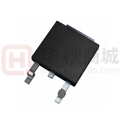
TO-252
Absolute Maximum Ratings (TC=25℃ unless otherwise specified)
Symbol
Parameter
Max.
Units
VDSS
Drain-Source Voltage
100
V
VGSS
Gate-Source Voltage
±20
V
TC = 25℃
15
A
TC = 100℃
6.5
A
60
A
6
mJ
44
W
3.4
℃/W
-55 to +175
℃
ID
Continuous Drain Current
IDM
Pulsed Drain Current
EAS
note1
Single Pulsed Avalanche Energy note2
TC = 25℃
PD
Power Dissipation
RθJC
Thermal Resistance, Junction to Case
TJ, TSTG
Operating and Storage Temperature Range
Sep 2022 Version1.0
1/8
www.ascendsemi.com
0755-86970486
�ASDM100N15KQ
100V N-Channel MOSFET
Electrical Characteristics (TJ=25℃ unless otherwise specified)
Symbol
Parameter
Test Condition
Min.
Typ.
Max.
Units
Off Characteristic
V(BR)DSS
Drain-Source Breakdown Voltage
VGS=0V, ID=250μA
100
-
-
V
IDSS
Zero Gate Voltage Drain Current
VDS=100V, VGS=0V,
-
-
1.0
μA
IGSS
Gate to Body Leakage Current
VDS=0V, VGS=±20V
-
-
±100
nA
1.0
1.5
2.5
V
On Characteristics
VGS(th)
Gate Threshold Voltage
VDS=VGS, ID=250μA
RDS(on)
Static Drain-Source on-Resistance
VGS=10V, ID=5A
-
92
110
mΩ
note3
VGS=4.5V, ID=3A
-
95
114
mΩ
-
744
-
pF
-
35
-
pF
-
11
-
pF
-
20
-
nC
-
2.8
-
nC
-
4
-
nC
-
6
-
ns
-
7
-
ns
-
21
-
ns
-
3
-
ns
Dynamic Characteristics
Ciss
Input Capacitance
Coss
Output Capacitance
Crss
Reverse Transfer Capacitance
Qg
Total Gate Charge
Qgs
Gate-Source Charge
Qgd
Gate-Drain(“Miller”) Charge
VDS=25V, VGS=0V,
f=1.0MHz
VDS=50V, ID=2A,
VGS=10V
Switching Characteristics
td(on)
Turn-on Delay Time
tr
Turn-on Rise Time
td(off)
Turn-off Delay Time
tf
VDS=50V, ID=3A,
RG=1.8Ω, VGS=10V
Turn-off Fall Time
Drain-Source Diode Characteristics and Maximum Ratings
IS
Maximum Continuous Drain to Source Diode Forward
Current
-
-
15
A
ISM
MaximumPulsedDraintoSourceDiodeForwardCurrent
-
-
60
A
VSD
Drain to Source Diode Forward
Voltage
-
-
1.2
V
trr
Body Diode Reverse Recovery Time
-
22
-
ns
Qrr
Body Diode Reverse Recovery
Charge
-
29
-
nC
VGS=0V, IS=10A
IF=10A,
dI/dt=100A/μs
Notes:1. Repetitive Rating: Pulse Width Limited by Maximum Junction Temperature
2. EAS condition : TJ=25℃,VDD=50V,VG=10V,L=0.5mH,Rg=25Ω,IAS=5A
3. Pulse Test: Pulse Width≤300μs, Duty Cycle≤0.5%
Sep 2022 Version1.0
2/8
www.ascendsemi.com
0755-86970486
�ASDM100N15KQ
100V N-Channel MOSFET
Typical Performance Characteristics
Figure 2: Typical Transfer Characteristics
Figure1: Output Characteristics
25
ID (A)
ID (A)
25
10V
20
20
4.5V
3.5V
15
15
3V
125℃
10
10
5
5
2.5V
VDS(V)
0
0
1
2
3
4
5
25℃
0
0
Figure 3: On-resistance vs. Drain Current
120
1.0
5.0
6.0
IS(A)
102
110
90
4.0
Figure 4 : Body Diode Characteristics
RDS(ON) (mΩ)
100
VGS (V)
3.0
2.0
VGS =4.5V
101
VGS =10V
100
125℃
25℃
0.6
VSD (V)
0.8
1.0
80
ID (A)
70
0
2
4
6
8
Figure 5: Gate Charge Characteristics
10
8
10-1
0
0.2
0.4
1.4
1.6
Figure 6: Capacitance Characteristics
VGS (V)
104
VDS=50V
ID =2A
C(pF)
Ciss
103
6
4
102
Coss
2
0
0
1.2
Qg (nC)
4
Sep 2022 Version1.0
8
12
3/8
16
20
Crss
101
0
10
VDS(V)
20
30
www.ascendsemi.com
40
50
0755-86970486
�ASDM100N15KQ
100V N-Channel MOSFET
Figure 8: Normalized on Resistance vs.
Junction Temperature
Figure 7: Normalized Breakdown Voltage vs.
Junction Temperature
VBR(DSS)
1.3
2.5
1.2
RDS (on)
2.0
1.1
1.5
1.0
1.0
0.9
0
-100
Tj (℃)
-50
0
50
100
150
200
I D(A)
12
2
10
10μs
1
10
100μs
Limited by R DS(on)
1ms
10ms
100ms
DC
Tc=25 ℃
Single pulse
10-1
10-2
0.1
Tj (℃)
-50
0
50
100
150
200
Figure 10: Maximum Continuous Drain Current
vs. Case Temperature
Figure 9: Maximum Safe Operating Area
100
0.5
-100
I D(A)
10
8
6
4
2
VDS (V)
10
1
0
100
Tc (℃)
0
25
50
75
100
125
150
175
Figure.11: Maximum Effective Transient Thermal
Impedance, Junction-to-Case
101
ZthJ-C ( ℃/W)
10-1
D=0.5
D=0.2
D=0.1
D=0.05
D=0.02
D=0.01
Single pulse
10-2
10-3 -6
10
10 -5
Sep 2022 Version1.0
10 -4
10-3
TP(s)
10-2
4/8
P DM
100
t1
t2
Notes:
1.Duty factor D=t1/t2
2.Peak T J=P DM *ZthJC +T C
10 -1
10 0
101
www.ascendsemi.com
0755-86970486
�ASDM100N15KQ
100V N-Channel MOSFET
Test Circuit
Figure1:Gate Charge Test Circuit & Waveform
Figure 2: Resistive Switching Test Circuit & Waveforms
Figure 3:Unclamped Inductive Switching Test Circuit & Waveforms
Sep 2022 Version1.0
5/8
www.ascendsemi.com
0755-86970486
�ASDM100N15KQ
100V N-Channel MOSFET
Ordering and Marking Information
Ordering Device No.
Marking
Package
Packing
Quantity
ASDM100N15KQ-R
100N15
TO-252
Tape&Reel
2500/ Reel
PACKAGE
MARKING
TO-252
Sep 2022 Version1.0
100N15
6/8
www.ascendsemi.com
0755-86970486
�ASDM100N15KQ
100V N-Channel MOSFET
TO-252
Sep 2022 Version1.0
7/8
www.ascendsemi.com
0755-86970486
�ASDM100N15KQ
100V N-Channel MOSFET
IMPORTANT NOTICE
ShenZhen Ascend Semiconductor incorporated MAKES NO WARRANTY OF ANY KIND, EXPRESS OR IMPLIED, WITH REGARDS TO THIS
DOCUMENT, INCLUDING, BUT NOT LIMITED TO, THE IMPLIED WARRANTIES OF MERCHANTABILITY AND FITNESS FOR A PARTICULAR
PURPOSE (AND THEIR EQUIVALENTS UNDER THE LAWS OF ANY JURISDICTION).
ShenZhen Ascend Semiconductor Incorporated and its subsidiaries reserve the right to make modifications, enhancements, improvements,
corrections or other changes without further notice to this document and any product described herein. ShenZhen Ascend Semiconductor
Incorporated does not assume any liability arising out of the application or use of this document or any product described herein; neither
does ShenZhen Ascend Semiconductor Incorporated convey any license under its patent or trademark rights, nor the rights of others. Any
Customer or user of this document or products described herein in such applications shall assume .
all risks of such use and will agree to hold Ascendsemi Incorporated and all the companies whose products are represented on ShenZhen
Ascend Semiconductor Incorporated website, harmless against all damages.
ShenZhen Ascend Semiconductor Incorporated does not warrant or accept any liability whatsoever in respect of any products purchased
through unauthorized sales channel. Should Customers purchase or use ShenZhen Ascend Semiconductor Incorporated products for any
unintended or unauthorized application, Customers shall indemnify and hold ShenZhen Ascend Semiconductor Incorporated and its
representatives harmless against all claims, damages, expenses, and attorney fees arising out of, directly or indirectly, any claim of personal
injury or death associated with such unintended or unauthorized application.
www.ascendsemi.com
Sep 2022 Version1.0
8/8
www.ascendsemi.com
0755-86970486
�
很抱歉,暂时无法提供与“ASDM100N15KQ-R”相匹配的价格&库存,您可以联系我们找货
免费人工找货- 国内价格
- 1+0.78000
- 100+0.72800
- 300+0.67600
- 500+0.62400
- 2000+0.59800
- 5000+0.58240
- 国内价格
- 5+0.68192
- 50+0.54713
- 150+0.47974
- 500+0.42920