ASDM100R066NQ
100V N-CHANNEL MOSFET
Features
Product Summary
100 V
VDS
RDS(on),Typ @ VGS=10V 5.9 mΩ
68
ID
A
Advanced Trench MOS Technology
Low Gate Charge
Low RDS(ON)
100% EAS Guaranteed
Green Device Available
Applications
Power Management in Desktop Computer or
DC/DC Converters.
Isolated DC/DC Converters in Telecom and
Industrial.
D
G
S
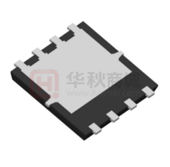
DFN5x6-8
Absolute Maximum Ratings
Symbol
Parameter
Rating
Units
VDS
Drain-Source Voltage
100
V
VGS
Gate-Source Voltage
±20
V
ID@TC=25℃
Continuous Drain Current1,6
68
A
ID@TC=70℃
Current1,6
48
A
140
A
61
mJ
35
A
108
W
Continuous Drain
IDM
Pulsed Drain
Current2
EAS
Single Pulse Avalanche Energy
IAS
Avalanche Current
Total Power
PD@TC=25℃
3
Dissipation4
TSTG
Storage Temperature Range
-55 to 150
℃
TJ
Operating Junction Temperature Range
-55 to 150
℃
Thermal Data
Symbol
RθJA
Parameter
Thermal Resistance Junction-Ambient
Typ.
1(t≦10s)
1
Thermal Resistance Junction-Ambient
RθJC
NOV 2018 Version1.1
Thermal Resistance
1/7
Junction-Case1
Max.
Unit
---
25
℃/W
---
55
℃/W
---
1.15
℃/W
www.ascendsemi.com
0755-86970486
�ASDM100R066NQ
100V N-CHANNEL MOSFET
Electrical Characteristics (TJ=25 ℃, unless otherwise noted)
Symbol
BVDSS
RDS(ON)
VGS(th)
IDSS
Parameter
Conditions
Drain-Source Breakdown Voltage
Min.
Typ.
Max.
Unit
V
VGS=0V , ID=250uA
100
---
---
Static Drain-Source
On-Resistance 2
VGS=10V , ID=13.5A
---
5.9
8
Static Drain-Source
On-Resistance2
VGS=4.5V , ID=11.5A
---
7.6
10.5
VGS=VDS , ID =250uA
1.2
---
2.3
VDS=80V , VGS=0V , TJ=25℃
---
---
1
VDS=80V , VGS=0V , TJ=55℃
---
---
5
Gate Threshold Voltage
Drain-Source Leakage Current
m
V
uA
IGSS
Gate-Source Leakage Current
VGS=±20V , VDS=0V
---
---
±100
nA
gfs
Forward Transconductance
VDS=5V , ID=20A
---
85
---
S
Qg
Total Gate Charge (10V)
---
45
---
Qg
Total Gate Charge (4.5V)
---
19.3
---
Qgs
Gate-Source Charge
---
9.5
---
Qgd
Gate-Drain Charge
---
4.8
---
Td(on)
Turn-On Delay Time
---
10
---
Tr
Td(off)
Tf
VDS=50V , VGS=10V , ID=13.5A
Rise Time
VDD=50V , VGS=10V , RG=3,
---
6.5
---
Turn-Off Delay Time
ID=13.5A
---
45
---
---
7.5
---
Fall Time
Ciss
Input Capacitance
Coss
Output Capacitance
Crss
Reverse Transfer Capacitance
VDS=50V , VGS=0V , f=1MHz
nC
ns
---
3320
---
---
605
---
---
20
---
Min.
Typ.
Max.
Unit
---
---
48
A
pF
Diode Characteristics
Symbol
IS
Parameter
Continuous Source Current
Conditions
1,5,6
VG=VD=0V , Force Current
Voltage2
VGS=0V , IS=1A , TJ=25℃
---
---
1.1
V
trr
Reverse Recovery Time
IF=13.5A , di/dt=100A/µs ,
---
33
---
nS
Qrr
Reverse Recovery Charge
TJ=25℃
---
150
---
nC
VSD
Diode Forward
Note :
1.The data tested by surface mounted on a 1 inch2 FR-4 board with 2OZ copper.
2.The data tested by pulsed , pulse width ≦ 300us , duty cycle ≦ 2%
3.The EAS data shows Max. rating . The test condition is V DD=25V,VGS=10V,L=0.3mH,IAS=35A
4.The power dissipation is limited by 150℃ junction temperature
5.The data is theoretically the same as ID and IDM , in real applications , should be limited by total power dissipation.
6.The maximum current rating is package limited.
NOV 2018 Version1.1
2/7
www.ascendsemi.com
0755-86970486
�ASDM100R066NQ
100V N-CHANNEL MOSFET
Typical Characteristics
Fig.1 Typical Output Characteristics
Fig.2 On-Resistance vs. G-S Voltage
Fig.3 Source-Drain Forward Characteristics
Fig.4 Gate-Charge Characteristics
Fig.5 Normalized VGS(th) vs. TJ
Fig.6 Normalized RDSON vs. TJ
NOV 2018 Version1.1
3/7
www.ascendsemi.com
0755-86970486
�ASDM100R066NQ
100V N-CHANNEL MOSFET
Fig.8 Safe Operating Area
Fig.7 Capacitance
Normalized Thermal Response (RθJC)
1
DUTY=0.5
0.2
0.1
0.1
0.05
0.02
0.01
0.01
P DM
T ON
SINGLE
T
D = TON/T
TJpeak = TC+P DMXRθJC
0.001
0.00001
0.0001
0.001
0.01
0.1
1
t , Pulse Width (s)
Fig.9 Normalized Maximum Transient Thermal Impedance
EAS=
VDS
90%
1
L x IAS2 x
2
BVDSS
BVDSS-VDD
BVDSS
VDD
IAS
10%
VGS
Td(on)
Tr
Td(off)
Ton
Tf
Toff
Fig.10 Switching Time Waveform
NOV 2018 Version1.1
4/7
VGS
Fig.11 Unclamped Inductive Switching Waveform
www.ascendsemi.com
0755-86970486
�ASDM100R066NQ
100V N-CHANNEL MOSFET
Ordering and Marking Information
Ordering Device No.
Marking
Package
Packing
Quantity
ASDM100R066NQ-R
100R066N
DFN5x6-8
Tape&Reel
4000/Reel
MARKING
PACKAGE
DFN5x6-8
NOV 2018 Version1.1
100R066N
5/7
www.ascendsemi.com
0755-86970486
�ASDM100R066NQ
100V N-CHANNEL MOSFET
DFN5x6-8 PACKAGE IN FORMATION
NOV 2018 Version1.1
6/7
www.ascendsemi.com
0755-86970486
�ASDM100R066NQ
100V N-CHANNEL MOSFET
IMPORTANT NOTICE
ShenZhen Ascend Semiconductor incorporated MAKES NO WARRANTY OF ANY KIND, EXPRESS OR IMPLIED, WITH REGARDS TO THIS
DOCUMENT, INCLUDING, BUT NOT LIMITED TO, THE IMPLIED WARRANTIES OF MERCHANTABILITY AND FITNESS FOR A PARTICULAR
PURPOSE (AND THEIR EQUIVALENTS UNDER THE LAWS OF ANY JURISDICTION).
ShenZhen Ascend Semiconductor Incorporated and its subsidiaries reserve the right to make modifications, enhancements, improvements,
corrections or other changes without further notice to this document and any product described herein. ShenZhen Ascend Semiconductor
Incorporated does not assume any liability arising out of the application or use of this document or any product described herein; neither
does ShenZhen Ascend Semiconductor Incorporated convey any license under its patent or trademark rights, nor the rights of others. Any
Customer or user of this document or products described herein in such applications shall assume .
all risks of such use and will agree to hold Ascendsemi Incorporated and all the companies whose products are represented on ShenZhen
Ascend Semiconductor Incorporated website, harmless against all damages.
ShenZhen Ascend Semiconductor Incorporated does not warrant or accept any liability whatsoever in respect of any products purchased
through unauthorized sales channel. Should Customers purchase or use ShenZhen Ascend Semiconductor Incorporated products for any
unintended or unauthorized application, Customers shall indemnify and hold ShenZhen Ascend Semiconductor Incorporated and its
representatives harmless against all claims, damages, expenses, and attorney fees arising out of, directly or indirectly, any claim of personal
injury or death associated with such unintended or unauthorized application.
www.ascendsemi.com
NOV 2018 Version1.1
7/7
www.ascendsemi.com
0755-86970486
�