ASDM40P90AKQ
-40V P-Channel MOSFET
Features
•
Super Low Gate Charge
•
100% EAS Guaranteed
•
Green Device Available
V DS
•
•
Excellent CdV/dt effect decline
Advanced high cell density Trench technology
R
Product Summary
I
DS(on),Typ
@ VGS=-10 V
D
-40
V
5.2
mΩ
-90
A
Application
•
Provides excellent RDSON for most synchronizations
•
Application of gate charge Buck converter
1
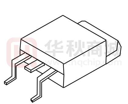
TO-252
Table 1.
Absolute Maximum Ratings (TA=25℃)
Symbol
Parameter
Value
Unit
VDS
Drain-Source Voltage (VGS=0V)
-40
V
VGS
Gate-Source Voltage (VDS=0V)
±20
V
ID (DC)
Drain Current-Continuous
-90
A
Drain Current-Continuous@ Current-Pulsed
-339
A
58
W
-55 To 175
℃
IDM (pluse)
PD
Maximum Power Dissipation
TJ,TSTG
Table 2.
Operating Junction and Storage Temperature Range
Thermal Characteristic
Symbol
Parameter
Max
Unit
R
JC
Thermal Resistance,Junction-to-Case
2.3
℃ /W
R
JA
Thermal Resistance,Junction-ambient
62
℃ /W
NOV 2021 Version1.0
1/7
www.ascendsemi.com
0755-86970486
�ASDM40P90AKQ
-40V P-Channel MOSFET
Table 3.
Electrical Characteristics (TA=25℃unless otherwise noted)
Symbol
Parameter
Conditions
Min
Typ
Max
Unit
BVDSS
Drain-Source Breakdown Voltage
VGS=0V ID=250μA
-40
IDSS
Zero Gate Voltage Drain Current(Tc=25℃)
VDS=-40V,VGS=0V
-1
μA
IGSS
Gate-Body Leakage Current
VGS=±20V,VDS=0V
±100
nA
VGS(th)
Gate Threshold Voltage
VDS=VGS,ID=250μA
-1.5
-2.5
V
VGS=-4.5V, ID=-15A
6.6
8
RDS(ON)
Drain-Source On-State Resistance
VGS=-10V, ID=-20A
5.2
6.5
On/Off States
-1.0
V
mΩ
Dynamic Characteristics
Ciss
Input Capacitance
Coss
Output Capacitance
5530
PF
454
PF
287
PF
16
nS
ID=-1A
17
nS
VGS =-10V
68
nS
31
nS
VDS=-20V,VGS=0V
f=1.0MHz
Crss
Reverse Transfer Capacitance
Switching Times
td(on)
Turn-on Delay Time
VDS=-20V
tr
Turn-on Rise Time
td(off)
Turn-Off Delay Time
RL =1.6Ω
tf
Turn-Off Fall Time
Qg
Total Gate Charge
VDS=-20V
118
nC
Qgs
Gate-Source Charge
VGS=-10V
13
nC
Qgd
Gate-Drain Charge
22
nC
-90
A
-1.2
V
ID=-8.0A
Source-Drain Diode Characteristics
ISD
Source-Drain Current(Body Diode)
VSD
Forward On Voltage
ton
Forward Turn-on Time
ISD=-8A,VGS=0V,
Intrinsic turn-on time is negligible(turn-on is dominated
Notes:
1.The data tested by surface mounted on a 1 inch2 FR-4 board with 2OZ copper.
2.The data tested by pulsed , pulse width≦300us , duty cycle≦2%
3.The power dissipation is limited by 175℃
junction temperature
4.The data is theoretically the same as ID and IDM , in real applications , should be limited by total power dissipation.
NOV 2021 Version1.0
2/7
www.ascendsemi.com
0755-86970486
�ASDM40P90AKQ
-40V P-Channel MOSFET
Typical Characteristics
NOV 2021 Version1.0
3/7
www.ascendsemi.com
0755-86970486
�ASDM40P90AKQ
-40V P-Channel MOSFET
NOV 2021 Version1.0
4/7
www.ascendsemi.com
0755-86970486
�ASDM40P90AKQ
-40V P-Channel MOSFET
Ordering and Marking Information
Ordering Device No.
Marking
Package
ASDM40P90AKQ-R
40P90A
TO-252
PACKAGE
Tape&Reel
Quantity
2500/Reel
MARKING
40P90A
TO-252
NOV 2021 Version1.0
Packing
5/7
www.ascendsemi.com
0755-86970486
�ASDM40P90AKQ
-40V P-Channel MOSFET
TO-252
D1
2
c
L
E
D3
L3
h
1
L2
L4
L1
D2
b
e
SYMBOL
MIN
Typ.
MAX
A
2.200
2.300
2.400
A1
0.000
b
0.640
0.690
0.740
0.460
0.520
0.580
6.500
6.600
6.700
D
D
A
MILLIMETER
D1
5.334 REF
D2
4.826 REF
3.166 REF
D3
E
6.000
A1
h
0.000
L
9.900
1.400
6/7
0.100
0.200
10.100
10.300
1.550
1.700
1.600 REF
L3
L4
6.200
2.888 REF
L1
L2
6.100
2.286 TYP
e
NOV 2021 Version1.0
0.127
0.600
0.800
1.000
1.100
1.200
1.300
www.ascendsemi.com
0755-86970486
�ASDM40P90AKQ
-40V P-Channel MOSFET
IMPORTANT NOTICE
ShenZhen Ascend Semiconductor incorporated MAKES NO WARRANTY OF ANY KIND, EXPRESS OR IMPLIED, WITH REGARDS TO THIS
DOCUMENT, INCLUDING, BUT NOT LIMITED TO, THE IMPLIED WARRANTIES OF MERCHANTABILITY AND FITNESS FOR A PARTICULAR
PURPOSE (AND THEIR EQUIVALENTS UNDER THE LAWS OF ANY JURISDICTION).
ShenZhen Ascend Semiconductor Incorporated and its subsidiaries reserve the right to make modifications, enhancements, improvements,
corrections or other changes without further notice to this document and any product described herein. ShenZhen Ascend Semiconductor
Incorporated does not assume any liability arising out of the application or use of this document or any product described herein; neither
does ShenZhen Ascend Semiconductor Incorporated convey any license under its patent or trademark rights, nor the rights of others. Any
Customer or user of this document or products described herein in such applications shall assume .
all risks of such use and will agree to hold Ascendsemi Incorporated and all the companies whose products are represented on ShenZhen
Ascend Semiconductor Incorporated website, harmless against all damages.
ShenZhen Ascend Semiconductor Incorporated does not warrant or accept any liability whatsoever in respect of any products purchased
through unauthorized sales channel. Should Customers purchase or use ShenZhen Ascend Semiconductor Incorporated products for any
unintended or unauthorized application, Customers shall indemnify and hold ShenZhen Ascend Semiconductor Incorporated and its
representatives harmless against all claims, damages, expenses, and attorney fees arising out of, directly or indirectly, any claim of personal
injury or death associated with such unintended or unauthorized application.
www.ascendsemi.com
NOV 2021 Version1.0
7/7
www.ascendsemi.com
0755-86970486
�
很抱歉,暂时无法提供与“ASDM40P90AKQ-R”相匹配的价格&库存,您可以联系我们找货
免费人工找货- 国内价格
- 1+1.90500
- 100+1.77800
- 300+1.65100
- 500+1.52400
- 2000+1.46050
- 5000+1.42240