ASDM65S035NX
650V N-Channel Super-Junction MOSFET
FEATURES
Product Summary
Ultra-fast body diode
V
DS
Very low FOM RDS(on)×Qg
R
DS(on),TYP
100% avalanche tested
ID
@ VGS=10 V
650
V
37
mΩ
72
A
RoHS compliant
APPLICATIONS
Switch Mode Power Supply (SMPS)
Uninterruptible Power Supply (UPS)
Power Factor Correction (PFC)
Absolute Maximum Ratings TC = 25ºC, unless otherwise noted
Parameter
Drain-Source Voltage (VGS = 0V)
Continuous Drain Current
TC = 25ºC
Symbol
Value
Unit
VDSS
650
V
72
ID
TC = 100ºC
Pulsed Drain Current
A
43.2
(note1)
Gate-Source Voltage
IDM
288
A
VGSS
±30
V
Single Pulse Avalanche Energy
(note2)
EAS
2185
mJ
Repetitive Avalanche Energy
(note2)
EAR
3.31
mJ
IAR
13.7
A
Avalanche Current
MOSFET dv/dt ruggedness, VDS = 0...480V
dv/dt
50
V/ns
Power Dissipation
PD
500
W
Continuous Body Diode Current
IS
61
A
Pulsed Diode Forward Current
(note1)
ISM
216
Reverse diode dv/dt
(note3)
dv/dt
50
V/ns
Maximum diode commutation speed
(note3)
dif/dt
900
A/us
TJ, Tstg
-55~+150
ºC
Symbol
Value
Unit
Thermal Resistance, Junction-to-Case
RthJC
0.25
Thermal Resistance, Junction-to-Ambient
RthJA
62
Operating Junction and Storage Temperature Range
Thermal Resistance
Parameter
ºC/W
NOV 2020 Version1.0
1/8
www.ascendsemi.com
0755-86970486
�ASDM65S035NX
650V N-Channel Super-Junction MOSFET
Specifications TJ = 25ºC, unless otherwise noted
Value
Parameter
Symbol
Test Conditions
Unit
Min.
Typ.
Max.
VGS = 0V, ID = 250µA
650
--
--
VDS = 650V, VGS = 0V, TJ = 25ºC
--
--
10
VDS = 650V, VGS = 0V, TJ = 150ºC
--
--
10000
IGSS
VGS = ±30V
--
--
±100
nA
Gate-Source Threshold Voltage
VGS(th)
VDS = VGS, ID = 250µA
3
3.9
5
V
Drain-Source On-Resistance
R DS(on)
VGS = 10V, ID = 36A
--
37
40
mΩ
f = 1.0MHz open drain
--
0.3
--
Ω
--
9600
--
--
271
--
Static
Drain-Source Breakdown Voltage
V(BR)DSS
Zero Gate Voltage Drain Current
IDSS
Gate-Source Leakage
Gate resistance
RG
V
μA
Dynamic
Input Capacitance
Ciss
VGS = 0V,
VDS = 100V, f
= 1.0MHz
Output Capacitance
Coss
Reverse Transfer Capacitance
Crss
--
16.2
--
Total Gate Charge
Qg
--
165
--
Gate-Source Charge
Qgs
--
50
--
Gate-Drain Charge
Qgd
--
70
--
Turn-on Delay Time
td(on)
--
103
--
Turn-on Rise Time
tr
--
83
--
Turn-off Delay Time
td(off)
--
543
--
--
93
--
--
1.0
1.5
V
--
242
--
ns
--
1.45
--
μC
--
12
--
A
Turn-off Fall Time
VDD = 520V, ID = 50A,
VGS = 10V
VDD = 400V, ID = 50A,
RG = 25Ω
tf
pF
nC
ns
Drain-Source Body Diode Characteristics
Body Diode Voltage
VSD
Reverse Recovery Time
trr
Reverse Recovery Charge
Qrr
Peak Reverse Recovery Current
Irrm
TJ = 25ºC, ISD = 36A, VGS = 0V
VR = 400V, IF = 36A,
diF/dt = 100A/μs
Notes
1.
Repetitive Rating: Pulse width limited by maximum junction temperature
2.
IAS = 13.7A, VDD = 50V, RG = 25Ω, Starting TJ = 25°C
3.
Identical low side and high side switch with identical R G
NOV 2020 Version1.0
2/8
www.ascendsemi.com
0755-86970486
�ASDM65S035NX
650V N-Channel Super-Junction MOSFET
Typical Characteristics TJ = 25ºC, unless otherwise noted
Figure 2. Transfer Characteristics
Figure 1. Output Characteristics
300
300
20V
10V
8V
7V
6V
5.5V
5V
200
150
VDS = 20V
250
ID, Drain Current (A)
ID, Drain Current (A)
250
TJ = 25ºC
200
150
100
100
50
TJ = 150ºC
50
0
0
5
10
15
0
20
0
2
6
8
10
Figure 4. Capacitance
Figure 3. On-Resistance vs. Drain Current
0.06
105
VGS = 0
f = 1MHz
VGS = 10V
TJ = 25ºC
Ciss
0.05
104
Capacitance (pF)
RDS(on), On-Resistance (Ω)
4
VGS, Gate-to-Source Voltage (V)
VDS, Drain-to-Source Voltage (V)
0.04
0.03
103
Coss
102
Crss
101
0.02
0
10
20
30
40
50
0
60
200
300
400
500
600
VDS, Drain-to-Source Voltage (V)
ID, Drain Current (A)
Figure 6. Body Diode Forward Voltage
Figure 5. Gate Charge
12
102
10
Is, Source Current (A)
VGS, Gate-to-Source Voltage (V)
100
VDD = 120V
8
VDD = 520V
6
4
TJ = 125ºC
101
TJ = 25ºC
100
2
10-1
0
0
50
100
150
Qg, Total Gate Charge (nC)
NOV 2020 Version1.0
3/8
200
0
0.5
1
1.5
VSD, Source-to-Drain Voltage (V)
www.ascendsemi.com
0755-86970486
2
�ASDM65S035NX
650V N-Channel Super-Junction MOSFET
Typical Characteristics TJ = 25ºC, unless otherwise noted
Figure 7. On-Resistance vs.
Junction Temperature
Figure 8. Breakdown voltage vs.
Junction Temperature
1.3
3
RDS(on), (Normalized)
VBR(DSS), (Normalized)
VGS = 10V
ID = 36A
2.5
2
1.5
1
0.5
ID = 250µA
1.2
1.1
1
0.9
0.8
0
-50
0
50
100
-30
150
60
90
120
150
Figure 10. Safe operation area for
Figure9 . Transient Thermal Impedance for
103
10-1
D = 0.5
D = 0.2
D = 0.1
D = 0.05
D = 0.02
D = 0.01
Single Pulse
10-2
ID, Drain Current(A)
100
ZthJC, Thermal Impedance (ºC/W)
30
TJ, Junction Temperature (ºC)
TJ, Junction Temperature (ºC)
10-3
10-5
0
102
101
100
tp = 1us
tp = 10us
tp = 100us
tp = 1ms
tp = 10ms
DC
10-1
10-2
10-4
10-3
10-2
Tp, Pulse Width (s)
NOV 2020 Version1.0
4/8
10-1
100
100
101
102
VDS, Drain-Source Voltage(V)
www.ascendsemi.com
103
0755-86970486
�ASDM65S035NX
650V N-Channel Super-Junction MOSFET
Figure A:Gate Charge Test Circuit and Waveform
Figure B:Resistive Switching Test Circuit and Waveform
Figure C:Unclamped Inductive Switching Test Circuit and Waveform
NOV 2020 Version1.0
5/8
www.ascendsemi.com
0755-86970486
�ASDM65S035NX
650V N-Channel Super-Junction MOSFET
Ordering and Marking Information
Ordering Device No.
Marking
Package
Packing
Quantity
ASDM65S035NX-T
65S035N
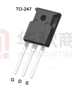
TO-247
Tube
30/Tube
MARKING
PACKAGE
TO-247
NOV 2020 Version1.0
65S035N
6/8
www.ascendsemi.com
0755-86970486
�ASDM65S035NX
650V N-Channel Super-Junction MOSFET
TO-247
Unit:mm
Unit:mm
Symbol
Min.
Nom
Max.
Symbol
Min.
Nom.
Max.
A
4.80
5.00
5.20
E
15.50
15.80
16.10
A1
2.21
2.41
2.61
E1
13.00
13.30
13.60
A2
1.85
2.00
2.15
E2
4.80
5.00
5.20
b
1.11
1.21
1.36
E3
2.30
2.50
2.70
b2
1.91
2.01
2.21
e
b4
2.91
3.01
3.21
L
19.62
19.92
20.22
c
0.51
0.61
0.75
L1
-
-
4.30
D
20.70
21.00
21.30
ФP
3.40
3.60
3.80
D1
16.25
16.55
16.85
ФP1
-
-
7.30
S
NOV 2020 Version1.0
7/8
5.44BSC
6.15BSC
www.ascendsemi.com
0755-86970486
�ASDM65S035NX
650V N-Channel Super-Junction MOSFET
IMPORTANT NOTICE
ShenZhen Ascend Semiconductor incorporated MAKES NO WARRANTY OF ANY KIND, EXPRESS OR IMPLIED, WITH REGARDS TO THIS
DOCUMENT, INCLUDING, BUT NOT LIMITED TO, THE IMPLIED WARRANTIES OF MERCHANTABILITY AND FITNESS FOR A PARTICULAR
PURPOSE (AND THEIR EQUIVALENTS UNDER THE LAWS OF ANY JURISDICTION).
ShenZhen Ascend Semiconductor Incorporated and its subsidiaries reserve the right to make modifications, enhancements, improvements,
corrections or other changes without further notice to this document and any product described herein. ShenZhen Ascend Semiconductor
Incorporated does not assume any liability arising out of the application or use of this document or any product described herein; neither
does ShenZhen Ascend Semiconductor Incorporated convey any license under its patent or trademark rights, nor the rights of others. Any
Customer or user of this document or products described herein in such applications shall assume .
all risks of such use and will agree to hold Ascendsemi Incorporated and all the companies whose products are represented on ShenZhen
Ascend Semiconductor Incorporated website, harmless against all damages.
ShenZhen Ascend Semiconductor Incorporated does not warrant or accept any liability whatsoever in respect of any products purchased
through unauthorized sales channel. Should Customers purchase or use ShenZhen Ascend Semiconductor Incorporated products for any
unintended or unauthorized application, Customers shall indemnify and hold ShenZhen Ascend Semiconductor Incorporated and its
representatives harmless against all claims, damages, expenses, and attorney fees arising out of, directly or indirectly, any claim of personal
injury or death associated with such unintended or unauthorized application.
www.ascendsemi.com
NOV 2020 Version1.0
8/8
www.ascendsemi.com
0755-86970486
�