ASDM30N150Q
30V N-Channel MOSFET
Features
⚫
⚫
⚫
⚫
⚫
High ruggedness
Low Gate Charge (Typ 143nC)
Improved dv/dt Capability
100% Avalanche Tested
Application:Synchronous Rectification,
Li Battery Protect Board, Inverter
Product Summary
V DS
30
V
R DS(on),Typ@ VGS=10 V
1.7
mΩ
ID
150
A
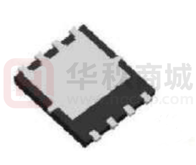
top view
DFN5x6-8
Absolute maximum ratings
Symbol
VDSS
Parameter
Drain to source voltage
=25oC)
ID
IDM
IDSM
Value
Unit
30
V
Continuous drain current (@Tc
150*
A
Continuous drain current (@Tc=100oC)
78*
A
600
A
Continuous drain current (@Ta=25oC)
30
A
Continuous drain current (@Ta=70oC)
24
A
± 20
V
Drain current pulsed(note 1)
VGS
Gate to source voltage
EAS
Single pulsed avalanche energy
(note 2)
576
mJ
EAR
Repetitive avalanche energy
(note 1)
57
mJ
dv/dt
Peak diode recovery dv/dt
(note 3)
5
V/ns
Total power dissipation (@Tc=25oC)
43
W
Total power dissipation (@Ta=25oC)
2.6
W
-55 ~ + 150
oC
Value
Unit
PD
TSTG, TJ
Operating junction temperature & storage temperature
*. Drain current is limited by junction temperature.
Thermal characteristics
Symbol
Parameter
Rthjc
Thermal resistance, Junction to case
1.8
oC/W
Rthja
Thermal resistance, Junction to ambient
62
oC/W
Note: Rthja is the sum of the junction-to-case and case-to-ambient thermal resistance where the case thermal reference is d
efined as the solder mounting surface of the drain pins. Rthjc is guaranteed by design while Rthca is determined by the user's
board design.
DEC 2018 Version2.0
1/9
www.ascendsemi.com
0755-86970486
�ASDM30N150Q
30V N-Channel MOSFET
Electrical characteristic ( TJ = 25oC unless otherwise specified )
Symbol
Parameter
Test conditions
Min.
Typ.
Max.
Unit
Off characteristics
BVDSS
ΔBVDSS
/ ΔTJ
IDSS
Drain to source breakdown voltage
Breakdown voltage temperature
coefficient
VGS=0V, ID=250uA
30
ID=250uA, referenced to 25oC
V
V/oC
0.02
VDS=30V, VGS=0V
1
uA
VDS=24V, TJ=125oC
50
uA
Gate to source leakage current, forward
VGS=20V, VDS=0V
100
nA
Gate to source leakage current, reverse
VGS=-20V, VDS=0V
-100
nA
2.4
V
Drain to source leakage current
IGSS
On characteristics
VGS(TH)
Gate threshold voltage
RDS(ON)
Drain to source on state resistance
Gfs
Forward transconductance
VDS=VGS, ID=250uA
1.2
VGS=4.5V, ID=30A,TJ=25oC
3.4
4.5
mΩ
VGS=10V, ID=30A,TJ=25oC
1.7
2.5
mΩ
VDS=5V, ID=30A
73
S
Dynamic characteristics
Ciss
Input capacitance
Coss
Output capacitance
Crss
Reverse transfer capacitance
td(on)
Turn on delay time
tr
td(off)
tf
6272
VGS=0V, VDS=15V, f=1MHz
1022
pF
718
20
VDS=15V, ID=30A, RG=4.7Ω,
VGS=10V
(note 4,5)
Rising time
Turn off delay time
58
ns
158
Fall time
77
Qg
Total gate charge
Qgs
Gate-source charge
Qgd
Rg
143
Gate-drain charge
VDS=24V, VGS=10V, ID=30A ,
IG=5mA
(note 4,5)
Gate resistance
VDS=0V, Scan F mode
4.2
17
nC
43
Ω
Source to drain diode ratings characteristics
Symbol
Parameter
Test conditions
Min.
IS
Continuous source current
ISM
Pulsed source current
Integral reverse p-n Junction
diode in the MOSFET
VSD
Diode forward voltage drop.
IS=45A, VGS=0V
trr
Reverse recovery time
Qrr
Reverse recovery charge
IS=30A, VGS=0V,
dIF/dt=100A/us
Typ.
Max.
Unit
150
A
600
A
1.4
V
26
ns
10
nC
※. Notes
1.
Repeatitive rating : pulse width limited by junction temperature.
2.
L =0.5mH, IAS =48A, VDD=30V, RG=25Ω, Starting TJ = 25oC
3.
ISD ≤30A, di/dt = 100A/us, VDD ≤ BVDSS, Staring TJ =25oC
4.
Pulse Test : Pulse Width ≤ 300us, duty cycle ≤ 2%.
5.
Essentially independent of operating temperature.
DEC 2018 Version2.0
2/9
www.ascendsemi.com
0755-86970486
�ASDM30N150Q
30V N-Channel MOSFET
Fig. 1. On-state characteristics
Fig. 2. Transfer Characteristics
Fig. 3. On-resistance variation vs.
drain current and gate voltage
Fig. 4. On-state current vs. diode
forward voltage
Fig 5. Breakdown voltage variation
vs. junction temperature
Fig. 6. On-resistance variation
vs. junction temperature
DEC 2018 Version2.0
3/9
www.ascendsemi.com
0755-86970486
�ASDM30N150Q
30V N-Channel MOSFET
Fig. 7. Gate charge characteristics
Fig. 9. Maximum safe operating area
Fig. 8. Capacitance Characteristics
Fig. 10. Maximum drain current vs. case
temperature
Fig. 11. Transient thermal response curve
DEC 2018 Version2.0
4/9
www.ascendsemi.com
0755-86970486
�ASDM30N150Q
30V N-Channel MOSFET
Fig. 12. Gate charge test circuit & waveform
Fig. 13. Switching time test circuit & waveform
VDS
90%
RL
RGS
VDS
VDD
VIN
10VIN
DUT
10%
10%
td(on)
tr
tON
td(off)
tf
tOFF
Fig. 14. Unclamped Inductive switching test circuit & waveform
DEC 2018 Version2.0
5/9
www.ascendsemi.com
0755-86970486
�ASDM30N150Q
30V N-Channel MOSFET
Fig. 15. Peak diode recovery dv/dt test circuit & waveform
DUT
+ V
DS
10V
VGS (DRIVER)
L
IS
di/dt
IS (DUT)
VDS
RG
IRRM
Diode reverse current
VDD
Diode recovery dv/dt
Same type
as DUT
10VGS
VDS (DUT)
*. dv/dt controlled by RG
*. Is controlled by pulse period
DEC 2018 Version2.0
6/9
VF
VDD
Body diode forward voltage drop
www.ascendsemi.com
0755-86970486
�ASDM30N150Q
30V N-Channel MOSFET
Ordering and Marking Information
Ordering Device No.
Marking
Package
Packing
Quantity
ASDM30N150Q-R
30N150
DFN5*6-8
Tape&Reel
4000/ Reel
PACKAGE
MARKING
DFN5*6-8
DEC 2018 Version2.0
30N150
7/9
www.ascendsemi.com
0755-86970486
�ASDM30N150Q
30V N-Channel MOSFET
DFN5*6-8
Symbol
A
A1
A2
b
C
D
D1
D2
e
E
E1
E2
L
L1
L2
L3
H
Ө
Dimensions in Millimeters
Min
Max
0.85
1.00
0.01
0.05
0.69
0.75
0.40
0.45
0.20
0.30
4.80
4.95
3.91
4.06
1.60
1.80
1.27 TYP
5.65
5.80
3.46
3.50
0.80
0.95
0.15
0.3
0.08
0.15
0.58
0.73
0.45
0.60
6.15
6.28
8°
12°
DEC 2018 Version2.0
Dimensions in Inches
Min
Max
0.033
0.039
0.000
0.002
0.027
0.030
0.016
0.018
0.008
0.012
0.189
0.195
0.154
0.160
0.063
0.071
0.05 TYP
0.222
0.228
0.136
0.138
0.031
0.037
0.006
0.012
0.003
0.006
0.023
0.029
0.018
0.024
0.242
0.247
8°
12°
8/9
www.ascendsemi.com
0755-86970486
�ASDM30N150Q
30V N-Channel MOSFET
IMPORTANT NOTICE
ShenZhen Ascend Semiconductor incorporated MAKES NO WARRANTY OF ANY KIND, EXPRESS OR IMPLIED, WITH REGARDS TO THIS
DOCUMENT, INCLUDING, BUT NOT LIMITED TO, THE IMPLIED WARRANTIES OF MERCHANTABILITY AND FITNESS FOR A PARTICULAR
PURPOSE (AND THEIR EQUIVALENTS UNDER THE LAWS OF ANY JURISDICTION).
ShenZhen Ascend Semiconductor Incorporated and its subsidiaries reserve the right to make modifications, enhancements, improvements,
corrections or other changes without further notice to this document and any product described herein. ShenZhen Ascend Semiconductor
Incorporated does not assume any liability arising out of the application or use of this document or any product described herein; neither
does ShenZhen Ascend Semiconductor Incorporated convey any license under its patent or trademark rights, nor the rights of others. Any
Customer or user of this document or products described herein in such applications shall assume .
all risks of such use and will agree to hold Ascendsemi Incorporated and all the companies whose products are represented on ShenZhen
Ascend Semiconductor Incorporated website, harmless against all damages.
ShenZhen Ascend Semiconductor Incorporated does not warrant or accept any liability whatsoever in respect of any products purchased
through unauthorized sales channel. Should Customers purchase or use ShenZhen Ascend Semiconductor Incorporated products for any
unintended or unauthorized application, Customers shall indemnify and hold ShenZhen Ascend Semiconductor Incorporated and its
representatives harmless against all claims, damages, expenses, and attorney fees arising out of, directly or indirectly, any claim of personal
injury or death associated with such unintended or unauthorized application.
www.ascendsemi.com
DEC 2018 Version2.0
9/9
www.ascendsemi.com
0755-86970486
�