ASDM20N16E
20V N-Channel MOSFET
Features
• Trench Power MV MOSFET technology
• High Speed switching
• Moisture Sensitivity Level 1
• Epoxy Meets UL 94 V-0 Flammability Rating
• Halogen Free
Product Summary
V DS
R
I
Application
•
PWM application
•
Load switch
DS(on),Typ
@ VGS=4.5 V
D
20
V
8.7
mΩ
16
A
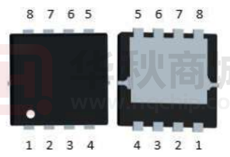
PDFN3.3x3.3-8
■ Absolute Maximum Ratings (TA =25℃ unless otherwise noted)
Parameter
Symbol
Limit
Unit
Drain-source Voltage
VDS
20
V
Gate-source Voltage
VGS
±10
V
16
TA=25℃
Drain Current
A
ID
10
TA=100℃
Pulsed Drain Current A
IDM
64
A
1
TA=25℃
Total Power Dissipation C
W
PD
0.4
TA=100℃
Junction and Storage Temperature Range
TJ ,TSTG
℃
-55~+150
■Thermal resistance
Parameter
Symbol
Typ
Max
Units
Thermal Resistance Junction-to-Ambient D
Steady-State
RθJA
29
36
℃/W
Thermal Resistance Junction-to-Case
Steady-State
RθJC
3.6
4.5
℃/W
NOV 2021 Version1.0
1/9
www.ascendsemi.com
0755-86970486
�ASDM20N16E
20V N-Channel MOSFET
■ Electrical Characteristics (TJ=25℃ unless otherwise noted)
Parameter
Symbol
Conditions
Min
Typ
Max
Units
Drain-Source Breakdown Voltage
BVDSS
VGS= 0V, ID=250μA
20
-
-
V
VDS=20V, VGS=0V
-
-
1
Zero Gate Voltage Drain Current
IDSS
VDS=20V, VGS=0V, Tj=150℃
-
-
100
IGSS
VGS= ±10V, VDS=0V
-
-
±100
nA
Gate Threshold Voltage
VGS(th)
VDS= VGS, ID=250μA
0.4
0.7
1.0
V
VGS=4.5V, ID=4.5A
-
8.7
11
Static Drain-Source On-Resistance
RDS(ON)
VGS=2.5V, ID=3.0A
-
12
15.5
Static Parameter
Gate-Body Leakage Current
μA
mΩ
Diode Forward Voltage
VSD
IS=4.5A, VGS=0V
-
0.9
1.2
V
Gate resistance
RG
f=1MHz, Open drain
-
3.3
-
Ω
Maximum Body-Diode Continuous Current
IS
-
-
16
A
Input Capacitance
Ciss
-
551
-
Output Capacitance
Coss
-
119
-
Reverse Transfer Capacitance
Crss
-
104
-
Total Gate Charge
Qg
-
11
-
Gate-Source Charge
Qgs
-
1
-
Gate-Drain Charge
Qgd
-
2
-
Reverse Recovery Charge
Qrr
-
4
-
nC
trr
-
10
-
ns
Turn-on Delay Time
tD(on)
-
3.5
-
Turn-on Rise Time
tr
-
26
-
Turn-off Delay Time
tD(off)
-
19
-
-
2.5
-
Dynamic Parameters
VDS=10V, VGS=0V, f=1MHz
pF
Switching Parameters
VGS=10V, VDS=10V, ID=4.5A
nC
IF=4.5A, di/dt=165A/us
Reverse Recovery Time
Turn-off fall Time
tf
VGS=10V, VDD=10V, ID=4.5A
RGEN=2.2Ω
ns
A. Repetitive rating; pulse width limited by max. junction temperature.
B. Pd is based on max. junction temperature, using junction-case thermal resistance.
C. The value of RθJA is measured with the device mounted on the minimum recommend pad size, in the still air environment with TA =25℃.
The maximum allowed junction temperature of 150℃. The value in any given application depends on the user's specific board design.
NOV 2021 Version1.0
2/9
www.ascendsemi.com
0755-86970486
�ASDM20N16E
20V N-Channel MOSFET
■Typical Electrical and Thermal Characteristics Diagrams
30
Tj=25℃
VDS=5V
3V
20
ID-Drain Current (A)
ID-Drain Current (A)
VGS=5V
4V
2.5V
20
2V
10
10
150℃
25℃
1.5V
0
0
0
1
2
0.5
3
1
VDS-Drain to Source Voltage (V)
Figure 1. Output Characteristics
2.5
10
VGS-Gate to Source Voltage (V)
Ciss
C-Capacitance (pF)
2
Figure 2. Transfer Characteristics
1000
Coss
100
Crss
10
0
5
10
15
20
VDS=10V
ID=4.5A
8 Tj=25℃
6
4
2
0
0
5
VDS-Drain to Source Voltage (V)
200
10
15
Qg-Total Gate Charge (nC)
Figure 3. Capacitance Characteristics
Figure 4. Gate Charge
1.6
ID=4.5A
Tj=25℃
RDS(on)-Drain to Source Resistance
Normalized
RDS(on)-Drain to Source resistance (mΩ)
1.5
Vgs-Gate to Source Voltage (V)
150
100
50
Vgs=10V
1.2
0.8
0.4
0
1
2
3
4
5
6
7
VGS-Gate to Source Voltage (V)
Figure 5. On-Resistance vs Gate to Source Voltage
NOV 2021 Version1.0
3/9
8
-75
-25
25
75
125
Tj-Junction Temperature (℃)
Figure 6. Normalized On-Resistance
www.ascendsemi.com
0755-86970486
175
�ASDM20N16E
10
20
Is-Reverse Drain Current (A)
RDS(on) -Drain to Source resistance (mΩ)
20V N-Channel MOSFET
15
VGS=2.5V
10
VGS=4.5V
5
Tj=25℃
0
0
150℃
1
0.1
2
4
6
8
0.2
10
0.4
Figure 7. RDS(on) VS Drain Current
BVDSS-MAX Drain to Source Voltage
Normalized
0.8
1
Figure 8. Forward characteristics of reverse diode
1.4
ID=250uA
ID=250uA
VGS(th)-Threshold Voltage
Normalized
1.2
1.05
1
0.95
0.9
-75
-25
25
75
125
1
0.8
0.6
0.4
0.2
175
-75
-25
25
75
125
175
Tj-Junction Temperature (℃)
Tj-Junction Temperature (℃)
Figure 9. Normalized breakdown voltage
Figure 10. Normalized Threshold voltage
2
5
Ptot-Power Dissipation (W)
4
ID-Drain Current (A)
0.6
Vsd- Source to Drain Voltage (V)
ID-Drain Current (A)
1.1
25℃
3
2
1
1.5
1
0.5
0
0
-50
0
50
100
TA-Ambient Temperature (℃)
Figure 11. Current dissipation
NOV 2021 Version1.0
4/9
150
-50
0
50
100
TA-Case Temperature (℃)
Figure 12. Power dissipation
www.ascendsemi.com
0755-86970486
150
�ASDM20N16E
20V N-Channel MOSFET
100
Zth(J-A)-Thermal Resistance (℃/W)
1000
ID-Drain-Source Current (A)
100
D=0.5
D=0.3
10
D=0.1
D=0.05
D=0.02
1
D=0.01
0.1
Single Pulse
10
10uS
Operation in this area is
limited by RDS(ON)
100uS
300uS
1mS
1
10mS
0.1
TJ(max)=150℃
DC
TA=25℃
0.01
0.0001 0.001
Single Pulse
0.01
0.1
1
10
100
1000
10000
0.01
0.01
Square Wave Pulse Durtion(S)
0.1
1
10
VDS-Drain to Source Voltage (V)
Figure 13. Maximum Transient Thermal Impedance
Figure 14. Safe Operation Area
■ Test Circuits & Waveforms
EAS=1/2*L*IAS2
Tp
VGS
D
S
L
Tp
G
IAS
A
D
VDD
ID
DUT
25Ω
BVDSS
Vds
G
S
Tp
VDS
Figure A. Unclamped Inductive Switching (UIS) Test Circuit & Waveform
NOV 2021 Version1.0
5/9
www.ascendsemi.com
0755-86970486
100
�ASDM20N16E
20V N-Channel MOSFET
D
R1
VGS
VGS (V)
Qg
R2
G
10V
S
C1
VDD
D
R3
VGS(pl)
DUT
G
IG
Qgd
Qgs
S
Charge (C)
Figure B. Gate Charge Test Circuit & Waveform
VDS
90%
L
90%
90%
D
DUT
Rg
C2
C1
VDD
Vds
G
S
R shunt
Vgs
VR
10%
10%
10%
VGS
tD(on)
tD(off)
tr
tf
Id=VR/R shunt
D
Rg
ISD
G
S
D
C1
C2
VDD
trr
DUT
G
S
R shunt
VR
25%IRRM
Qrr
L
IRRM
Figure D. Diode Recovery Test Circuit & Waveform
NOV 2021 Version1.0
6/9
www.ascendsemi.com
0755-86970486
�ASDM20N16E
20V N-Channel MOSFET
Ordering and Marking Information
Ordering Device No.
Marking
ASDM20N16E-R
20N16
Packing
Quantity
PDFN3.3x3.3-8
Tape&Reel
5000/Reel
MARKING
PACKAGE
PDFN3.3x3.3-8
NOV 2021 Version1.0
Package
20N16
7/9
www.ascendsemi.com
0755-86970486
�ASDM20N16E
20V N-Channel MOSFET
NOV 2021 Version1.0
8/9
www.ascendsemi.com
0755-86970486
�ASDM20N16E
20V N-Channel MOSFET
IMPORTANT NOTICE
ShenZhen Ascend Semiconductor incorporated MAKES NO WARRANTY OF ANY KIND, EXPRESS OR IMPLIED, WITH REGARDS TO THIS
DOCUMENT, INCLUDING, BUT NOT LIMITED TO, THE IMPLIED WARRANTIES OF MERCHANTABILITY AND FITNESS FOR A PARTICULAR
PURPOSE (AND THEIR EQUIVALENTS UNDER THE LAWS OF ANY JURISDICTION).
ShenZhen Ascend Semiconductor Incorporated and its subsidiaries reserve the right to make modifications, enhancements, improvements,
corrections or other changes without further notice to this document and any product described herein. ShenZhen Ascend Semiconductor
Incorporated does not assume any liability arising out of the application or use of this document or any product described herein; neither
does ShenZhen Ascend Semiconductor Incorporated convey any license under its patent or trademark rights, nor the rights of others. Any
Customer or user of this document or products described herein in such applications shall assume .
all risks of such use and will agree to hold Ascendsemi Incorporated and all the companies whose products are represented on ShenZhen
Ascend Semiconductor Incorporated website, harmless against all damages.
ShenZhen Ascend Semiconductor Incorporated does not warrant or accept any liability whatsoever in respect of any products purchased
through unauthorized sales channel. Should Customers purchase or use ShenZhen Ascend Semiconductor Incorporated products for any
unintended or unauthorized application, Customers shall indemnify and hold ShenZhen Ascend Semiconductor Incorporated and its
representatives harmless against all claims, damages, expenses, and attorney fees arising out of, directly or indirectly, any claim of personal
injury or death associated with such unintended or unauthorized application.
www.ascendsemi.com
NOV 2021 Version1.0
9/9
www.ascendsemi.com
0755-86970486
�
很抱歉,暂时无法提供与“ASDM20N16E-R”相匹配的价格&库存,您可以联系我们找货
免费人工找货