ASDM2305ZA
-20V P-CHANNEL MOSFET
Features
Product Summary
● High power and current handing capability
V
● Lead free product is acquired
● Surface mount package
DS
-20
V
45
mΩ
5.4
A
R DS(on),TYP@ VGS=-4.5 V
Application
ID
-
● Motor control and drive
● Battery management
● UPS (Uninterrupible Power Supplies)
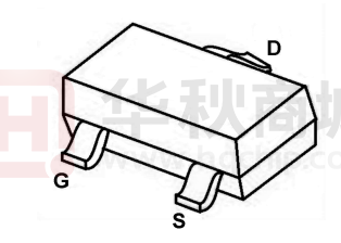
top view
D
G
S
P-Channel
SOT-23
ABSOLUTE MAXIMUM RATINGS TA = 25 °C, unless otherwise noted
ameter
Drain-Source Voltage
Gate-Source Voltage
Limit
- 20
± 12
VDS
VGS
Continuous Drain Current (TJ = 150 °C)
TC = 25 °C
TC = 70 °C
= 25 °C
= 70 °C
Continuous Source-Drain Diode Current
TC = 25 °C
TA = 25 °C
Maximum Power Dissipation
TC = 25 °C
TC = 70 °C
TA = 25 °C
TA = 70 °C
ID
- 3.3 a, b
- 21.6
A
- 5.4
- 0.8 a, b
IS
1.7
1.1
PD
W
0.96a, b
0.62a, b
- 50 to 150
260
TJ, Tstg
Operating Junction and Storage Temperature Range
Soldering Recommendations (Peak Temperature)
Notes:
a. Surface Mounted on 1" x 1" FR4 board.
b. t = 10 s.
V
- 5.4
- 4.3 TA
- 4.1a, b TA
IDM
Pulsed Drain Current
Unit
°C
THERMAL RESISTANCE RATINGS
Parameter
t ≤ 10 s
Steady State
a, b
Maximum Junction-to-Ambient
Maximum Junction-to-Foot (Drain)
Symbol
RthJA
RthJF
Typical
100
60
Maximum
130
75
Unit
°C/W
Notes:
a. Surface Mounted on 1" x 1" FR4 board.
b. Maximum under Steady State conditions is 175 °C/W.
NOV 2018 Version2.0
1/9
www.ascendsemi.com
0755-86970486
�ASDM2305ZA
-20V P-CHANNEL MOSFET
SPECIFICATIONS TJ = 25 °C, unless otherwise noted
Parameter
Symbol
Test Conditions
Min.
Static
Drain-Source Breakdown Voltage
VDS Temperature Coefficient
VDS
VGS = 0 V, ID = - 250 µA
- 20
ΔVDS/TJ
VGS(th) Temperature Coefficient
ΔVGS(th)/TJ
ID = - 250 µA
Gate-Source Threshold Voltage
VGS(th)
VDS = VGS, ID = - 250 µA
Gate-Source Leakage
IGSS
VDS = 0 V, VGS = ± 8 V
Zero Gate Voltage Drain Current
IDSS
On-State Drain Currenta
ID(on)
Drain-Source On-State Resistancea
RDS(on)
Forward Transconductancea
Dynamicb
Input Capacitance
Ciss
Output Capacitance
Coss
Reverse Transfer Capacitance
Crss
Total Gate Charge
Qg
Gate-Source Charge
Qgs
Gate-Drain Charge
Qgd
Gate Resistance
Rg
gfs
tr
Rise Time
td(off)
Turn-Off DelayTime
Fall Time
Turn-On Delay Time
- 0.45
Drain-Source Body Diode Characteristics
Continuous Source-Drain Diode Current
Pulse Diode Forward Currenta
Body Diode Voltage
V
nA
VDS = - 16 V, VGS = 0 V
-1
VDS = - 16 V, VGS = 0 V, TJ = 55 °C
- 10
45
50
VGS = - 2.5 V, ID = - 3.4 A
60
75
VGS = - 1.8 V, ID = - 2.0 A
84
88
VDS = - 5 V, ID = - 4.1 A
8
VDS = - 4 V, VGS = 0 V, f = 1 MHz
163
VDS = - 4 V, VGS = - 4.5 V, ID = - 4.1 A
107
7.8
15
4.5
9
416
VDS = - 4 V, VGS = - 2.5 V, ID = - 4.1 A
pF
1.2
1.4
VDD = - 4 V, RL = 1.2 Ω
ID ≅ - 3.3 A, VGEN = - 4.5 V, Rg = 1 Ω
7
14
13
20
35
53
48
td(on)
5
10
11
17
VDD = - 4 V, RL = 1.2 Ω
ID ≅ - 3.3 A, VGEN = - 8 V, Rg = 1 Ω
22
33
16
24
TC = 25 °C
-5.4
ISM
VSD
trr
Body Diode Reverse Recovery Charge
Qrr
Reverse Recovery Fall Time
ta
Reverse Recovery Rise Time
tb
nC
1.6
f = 1 MHz
20
Body Diode Reverse Recovery Time
mΩ
S
10
IS
µA
A
-5
tf
Fall Time
- 0.8
± 100
tf
td(off)
Turn-Off DelayTime
mV/°C
2.1
VDS ≤ - 5 V, VGS = - 4.5 V
VGS = - 4.5 V, ID = - 4.1 A
Unit
V
32
tr
Rise Time
Max.
- 55
td(on)
Turn-On Delay Time
Typ.
- 10
IF = - 3.3 A
IF = - 3.3 A, dI/dt = 100 A/µs, TJ = 25 °C
Ω
ns
A
- 0.8
- 1.2
V
33
50
ns
14
21
nC
14
19
ns
Notes:
a. Pulse test; pulse width ≤ 300 µs, duty cycle ≤ 2 %.
b. Guaranteed by design, not subject to production testing.
Stresses beyond those listed under “Absolute Maximum Ratings” may cause permanent damage to the device. These are stress ratings only, and functional operation
of the device at these or any other conditions beyond those indicated in the operational sections of the specifications is not implied. Exposure to absolute maximum
rating conditions for extended periods may affect device reliability.
NOV 2018 Version2.0
2/9
www.ascendsemi.com
0755-86970486
�ASDM2305ZA
-20V P-CHANNEL MOSFET
TYPICAL CHARACTERISTICS 25 °C, unless otherwise noted
12
VGS = 4.5 V thru 2 V
9
9
6
I D - Drain Current (A)
I D - Drain Current (A)
12
VGS = 1.5 V
3
6
3
TC = 125 °C
TC = 25 °C
VGS = 0.5 V
VGS = 1 V
0
0.0
0.5
1.0
1.5
2.0
2.5
3.0
3.5
TC = - 55 °C
0
0.0
4.0
0.5
VDS - Drain-to-Source Voltage (V)
1.0
1.5
2.0
VGS - Gate-to-Source Voltage (V)
Output Characteristics
Transfer Characteristics
1200
0.10
900
0.08
C - Capacitance (pF)
RDS(on) - On-Resistance (Ω)
VGS = 1.8 V
VGS = 2.5 V
0.06
600
Ciss
Coss
300
0.04
VGS = 4.5 V
Crss
0
0.02
0
2
4
8
0
10
2
6
8
VDS - Drain-to-Source Voltage (V)
ID - Drain Current (A)
On-Resistance vs. Drain Current and Gate Voltage
Capacitance
1.5
4.5
2.7
VDS = 6.4 V
1.8
VDS = 2.5 V, ID = 3.4 A
1.3
(Normalized)
VDS = 4 V
RDS(on) - On-Resistance
VGS - Gate-to-Source Voltage (V)
ID = 4.1 A
3.6
1.1
VDS = 4.5 V, ID = 4.1 A
0.9
0.9
0.0
0.0
1.5
3.0
4.5
6.0
Qg - Total Gate Charge (nC)
Gate Charge
NOV 2018 Version2.0
3/9
7.5
9.0
0.7
- 50
- 25
0
25
50
75
100
125
150
TJ - Junction Temperature (°C)
On-Resistance vs. Junction Temperature
www.ascendsemi.com
0755-86970486
�ASDM2305ZA
-20V P-CHANNEL MOSFET
TYPICAL CHARACTERISTICS 25 °C, unless otherwise noted
100
0.10
10
TJ = 150 °C
TJ = 25 °C
1
0.1
0.0
0.08
RDS(on) - On-Resistance (Ω)
I S - Source Current (A)
ID = 4.1 A
0.06
TA = 125 °C
0.04
TA = 25 °C
0.02
0.00
0.2
0.4
0.6
0.8
1.0
0
1.2
2
6
8
VSD - Source-to-Drain Voltage (V)
VGS - Gate-to-Source Voltage (V)
Source-Drain Diode Forward Voltage
On-Resistance vs. Gate-to-Source Voltage
30
0.7
0.6
ID = 250 µA
Power (W)
VGS(th) (V)
20
0.5
0.4
10
0.3
0.2
- 50
- 25
0
25
50
75
100
125
150
0
0.001
0.01
0.1
1
10
TJ - Temperature (°C)
Time (s)
Threshold Voltage
Single Pulse Power, Junction-to-Ambient
100
100
I D - Drain Current (A)
Limited by RDS(on)*
10
1 ms
1
10 ms
100 ms
1s
10 s
DC
0.1
TA = 25 °C
Single Pulse
0.01
0.1
1
10
VDS - Drain-to-Source Voltage (V)
* VGS > minimum VGS at which RDS(on) is specified
Safe Operating Area, Junction-to-Ambient
NOV 2018 Version2.0
4/9
www.ascendsemi.com
0755-86970486
�ASDM2305ZA
-20V P-CHANNEL MOSFET
TYPICAL CHARACTERISTICS
25 °C, unless otherwise noted
6.0
I D - Drain Current (A)
4.5
3.0
1.5
0.0
0
25
50
75
100
125
150
TC - Case Temperature (°C)
2.0
1.00
1.5
0.75
Power (W)
Power (W)
Current Derating*
1.0
0.5
0.50
0.25
0.0
0.00
0
25
50
75
100
TC - Case Temperature (°C)
Power, Junction-to-Case
125
150
0
25
50
75
100
125
150
TA - Ambient Temperature (°C)
Power, Junction-to-Ambient
* The po er dissipation PD is based on TJ(max) = 150 °C, using junction-to-case thermal resistance, and is more useful in settling the upper
dissipation limit for cases where additional heatsinking is used. It is used to determine the current rating, when this rating falls below the package
limit.
NOV 2018 Version2.0
5/9
www.ascendsemi.com
0755-86970486
�ASDM2305ZA
-20V P-CHANNEL MOSFET
TYPICAL CHARACTERISTICS 25 °C, unless otherwise noted
1
Normalized Effective Transient
Thermal Impedance
Duty Cycle = 0.5
0.2
0.1
0.1
0.05
Notes:
0.02
PDM
t1
0.01
Single Pulse
t2
1. Duty Cycle, D =
t1
t2
2. Per Unit Base = RthJA = 175 °C/W
3. TJM - TA = PDMZthJA(t)
4. Surface Mounted
0.001
10 -4
10 -3
10 -2
10 -1
1
10
100
1000
Square Wave Pulse Duration (s)
Normalized Thermal Transient Impedance, Junction-to-Ambient
1
Normalized Effective Transient
Thermal Impedance
Duty Cycle = 0.5
0.2
0.1
0.1
0.05
0.02
Single Pulse
0.01
10 -4
10 -3
10 -2
10 -1
1
Square Wave Pulse Duration (s)
Normalized Thermal Transient Impedance, Junction-to-Foot
NOV 2018 Version2.0
6/9
www.ascendsemi.com
0755-86970486
�ASDM2305ZA
-20V P-CHANNEL MOSFET
Ordering and Marking Information
Ordering Device No.
ASDM2305ZA-R
Package
2305
SOT-23
Packing
Quantity
Tape&Reel
3000/Reel
MARKING
PACKAGE
2305
SOT-23
NOV 2018 Version2.0
Marking
7/9
Lot Number
www.ascendsemi.com
0755-86970486
�ASDM2305ZA
-20V P-CHANNEL MOSFET
Symbol
Dimensions in Millimeters
Min
Max
Dimensions in Inches
Min
Max
A
0.90
1.15
0.035
0.045
A1
0.00
0.10
0.000
0.004
A2
0.90
1.05
0.035
0.041
b
0.30
0.55
0.012
0.022
C
0.08
0.15
0.003
0.006
D
2.80
3.00
0.110
0.118
E
1.20
1.40
0.047
0.055
0.95 TYP
e
0.037 TYP
e1
1.80
2.00
0.071
0.079
H
2.25
2.55
0.089
0.100
L
0.30
0.50
0.012
0.020
θ
0∘
8∘
0∘
8∘
NOV 2018 Version2.0
8/9
www.ascendsemi.com
0755-86970486
�ASDM2305ZA
-20V P-CHANNEL MOSFET
IMPORTANT NOTICE
ShenZhen Ascend Semiconductor incorporated MAKES NO WARRANTY OF ANY KIND, EXPRESS OR IMPLIED, WITH REGARDS TO THIS
DOCUMENT, INCLUDING, BUT NOT LIMITED TO, THE IMPLIED WARRANTIES OF MERCHANTABILITY AND FITNESS FOR A PARTICULAR
PURPOSE (AND THEIR EQUIVALENTS UNDER THE LAWS OF ANY JURISDICTION).
ShenZhen Ascend Semiconductor Incorporated and its subsidiaries reserve the right to make modifications, enhancements, improvements,
corrections or other changes without further notice to this document and any product described herein. ShenZhen Ascend Semiconductor
Incorporated does not assume any liability arising out of the application or use of this document or any product described herein; neither
does ShenZhen Ascend Semiconductor Incorporated convey any license under its patent or trademark rights, nor the rights of others. Any
Customer or user of this document or products described herein in such applications shall assume .
all risks of such use and will agree to hold Ascendsemi Incorporated and all the companies whose products are represented on ShenZhen
Ascend Semiconductor Incorporated website, harmless against all damages.
ShenZhen Ascend Semiconductor Incorporated does not warrant or accept any liability whatsoever in respect of any products purchased
through unauthorized sales channel. Should Customers purchase or use ShenZhen Ascend Semiconductor Incorporated products for any
unintended or unauthorized application, Customers shall indemnify and hold ShenZhen Ascend Semiconductor Incorporated and its
representatives harmless against all claims, damages, expenses, and attorney fees arising out of, directly or indirectly, any claim of personal
injury or death associated with such unintended or unauthorized application.
www.ascendsemi.com
NOV 2018 Version2.0
9/9
www.ascendsemi.com
0755-86970486
�